Article

Measurement of Ion Energy Distribution and Deposition of Ti Thin Films Using ABPPS Technology on Glass Substrate

1
Fundamental Technology Research Division, Institute of Plasma Technology, Korea Institute of Fusion Energy, 37 Dongjangsan-ro, Gunsan-si 54004, Korea
2
Plasma E.I. Convergence Research Center, Korea Institute of Fusion Energy, 37 Dongjangsan-ro, Gunsan-si 54004, Korea
*
Author to whom correspondence should be addressed.
Coatings 2021, 11(8), 904; https://doi.org/10.3390/coatings11080904
Submission received: 16 July 2021 / Revised: 26 July 2021 / Accepted: 26 July 2021 / Published: 28 July 2021
(This article belongs to the Special Issue Surface Modification by Plasma-Based Processes)

Abstract

:
Ion energy distributions (IEDs) play an important role in material processes and thin film deposition. We developed a newly designed multistep pulsed power supply (modulator) for the asymmetric bipolar pulsed power sputtering (ABPPS) technology and studied the effect of reverse bias voltage in improving the properties of thin films through Ti deposition. Using an ion energy analyzer, we confirmed IEDs and relative ion intensity under a reverse bias voltage of the modulator at the substrate position. A dense plasma was generated near the sputter target at reverse bias voltages above 300 V. Experiments were conducted by varying the bias voltage applied to the sputter target and the duty cycle of the modulator. Our results demonstrate that the in-house-built ABPPS system can be used to clean the sample surfaces without requiring additional energy sources or substrate bias and that thin films prepared using this system have a smoother surface than those prepared by conventional sputtering.

1. Introduction

Sputtering methods have been widely used in many industrial applications owing to their significant advantages over other deposition systems, such as simple implementation, improvement in film uniformity over large areas, and easy control of the film thickness. The conventional direct current (DC) sputtering technology has two typical drawbacks: (i) low sputtering yield due to the low plasma density and (ii) arcing due to the deposition of insulating layers on the target surface. To overcome these drawbacks, many sputtering-based deposition processes have adopted the pulsed DC magnetron sputtering technology [1,2,3,4]. In particular, the arcing phenomenon during the DC sputtering of an insulating target can cause serious substrate damage. The pulsed DC magnetron sputtering technology can be used to eliminate arcing during reactive sputtering and improve the coating structure and properties by varying the pulsing parameters [4,5].
Asymmetric bipolar pulsed power can be used for the reactive deposition of oxide and nitride compounds [5,6,7,8]. In this case, the polarity of the power periodically switches from negative (sputter voltage) to positive (reverse bias voltage). A reverse bias voltage is applied to the sputter target for a short duration (approximately 10 μs or less). At this time, electrons are accelerated to the target, and the arcing at the sputter target can be alleviated through the release of the positive charge build-up. The effect of reverse bias voltage has been studied in the context of arcing due to target poisoning.
Substrate bias plays an important role in the surface characteristics of a substrate [9,10,11]. It affects the surface morphology, chemical composition, wetting behavior, and microstructure properties of the sample surface. At the beginning of the reverse bias voltage application, there is a change in the high-energy ions generated by the overshoot of the positive voltage for an extremely short duration [7,12]. The results of analyses conducted using a Langmuir probe and an ion energy analyzer (IEA) have shown that high-energy ions are the result of increased plasma potential when a target is positively biased (reverse bias voltage) [13]. As mentioned previously, the surface characteristics of a substrate can be altered by the high-energy ions generated by the reverse bias voltage instead of the substrate bias. However, the effect of surface modification may be insufficient when the amplitude of the reverse bias voltage is low and the period is short. Barshilia and Rajam applied substrate bias to improve the mechanical properties of a coating material despite the application of bipolar pulse power [14].
Clearly, the reverse bias voltage plays an important role in the treatment of sample surfaces. In this study, a modulator, aimed for a longer surface treatment, was constructed based on an insulated gate bipolar transistor (IGBT). To confirm the ion energy distributions (IEDs) and relative intensity under the reverse bias voltage of the modulator, we employed an IEA and the Langmuir probe. We focused on the treatment effect of the ion energy for a relatively longer period (from tens of microseconds to tens of milliseconds) than that reported previously. The thin-film properties could be altered without requiring additional energy sources via the easy control of the ion energy supplied to the substrate. The surface characteristics of the Ti thin films deposited under different modulator conditions were also investigated. A surface analysis of the modified samples was performed using various analysis techniques. The rest of this paper is organized as follows. Section 2 presents the experimental setup of an asymmetric bipolar pulsed power sputtering (ABPPS) system and the IEA used to measure the IEDs. In Section 3, the experimental results are discussed in terms of the reverse bias voltage, called the extractor voltage. The conclusions are presented in Section 4.

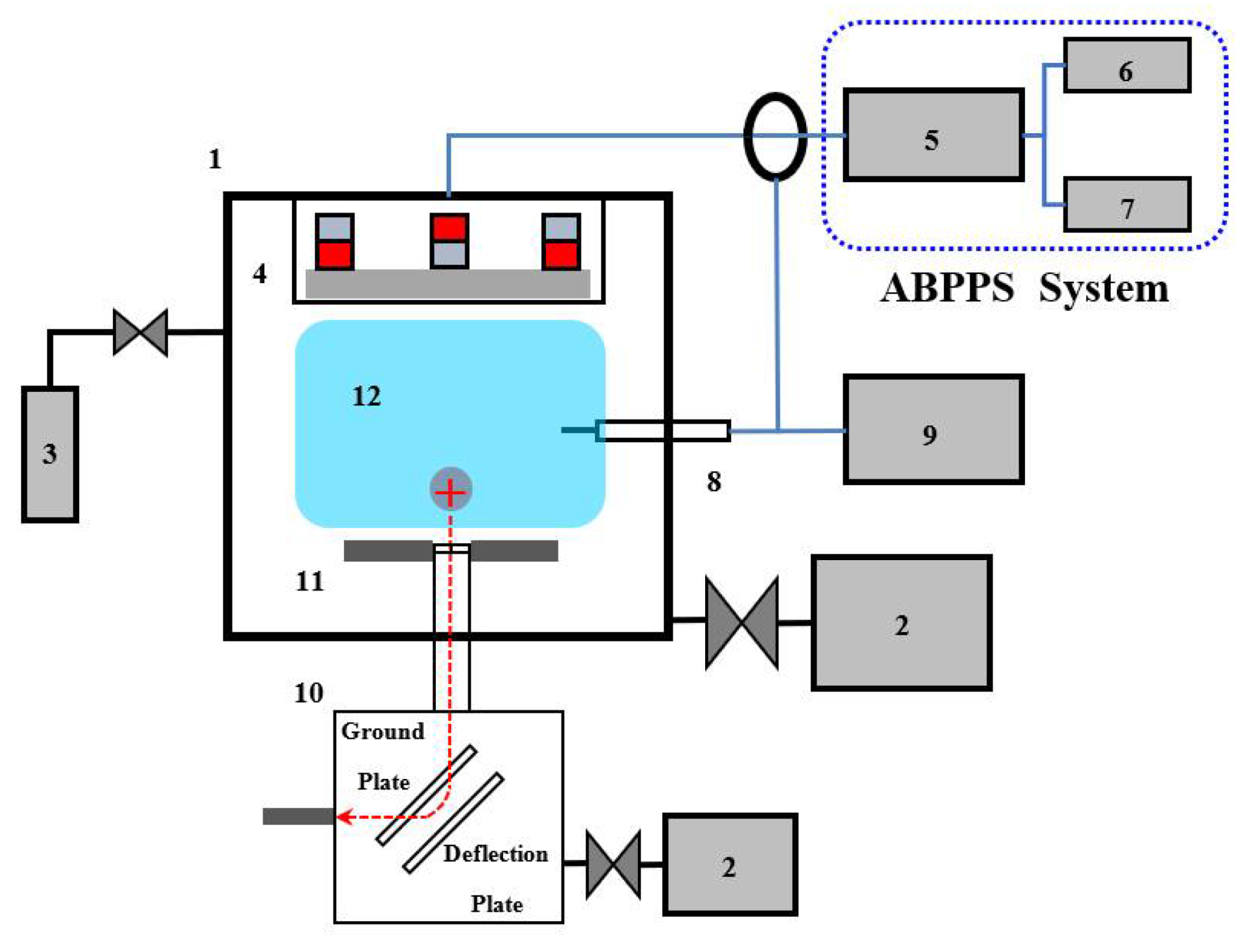
2. Experimental Details

Figure 1 shows a schematic of the experimental device for the ABPPS. The device comprises a magnetron sputter (in-house-built device), an ABPPS system, and an IEA (in-house-built device). A stainless-steel vacuum chamber with a base pressure of 1.3 × 10⁴ Pa was filled with argon to a working pressure range of 0.13–0.67 Pa. A 99.995% pure Ti disc with a diameter of 4 inch was used as the sputtering target. A thin planar stainless-steel disc with a diameter of 100 mm was used as the substrate holder and was attached to the bottom of the vacuum chamber. The substrate was located 100 mm from the target. The glass sample was loaded onto the substrate after cleaning with methanol.
The ABPPS system was designed and constructed in-house to better control the ion energy. The IGBT type (1700 V, 430 A) bipolar pulse modulator (in-house-built device) included in the ABPPS system was connected to negative and positive DC power supplies. The on–off operation of the modulator was controlled using an external transistor–transistor logic (TTL) pulse. The detailed circuit of the modulator is not presented herein.
The IEDs were measured using an in-house-built IEA, comprising a pair of deflecting plates and a particle detector such as a channel electron multiplier (MAGNUM 5900, BURLE, Lancaster, CA, USA). The IEA system was separated from the main plasma source chamber by a pin hole (0.5 mm in diameter) plate and implemented at a pressure of less than 1.33 × 10⁻⁴ Pa for optimum operation of the CEM. The ion energy detected by the CEM was linearly associated with the deflecting plate voltage between the two parallel plates [15].
We used various analysis techniques to characterize the thin film surfaces. To explain the cleaning effect of the sample surface, the water contact angles were measured using the static sessile drop method with a contact angle goniometer (DSA100, KRUSS, Hamburg, Germany). The crystal structure, surface morphologies, and cross-sectional view of the Ti thin films were investigated using XRD (NL/EMPYREAN, Malvern Panalytical, Malvern, UK), AFM (NX10, Park Systems, Suwon, Korea), and FESEM (SIGMA, Carl Zeiss, Oberkochen, Germany), respectively.

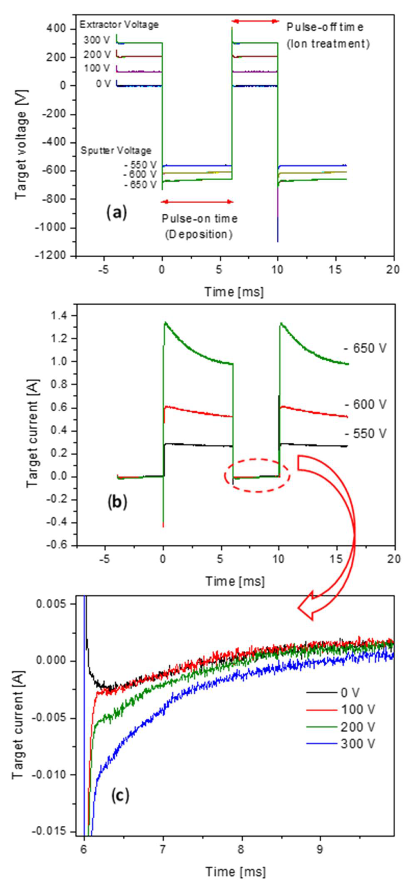
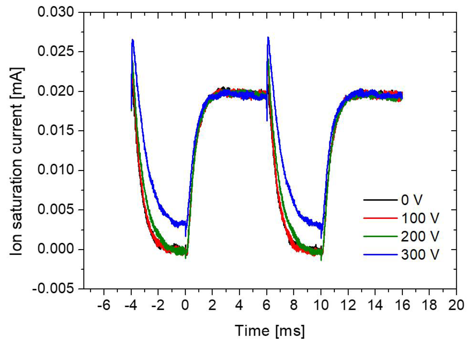
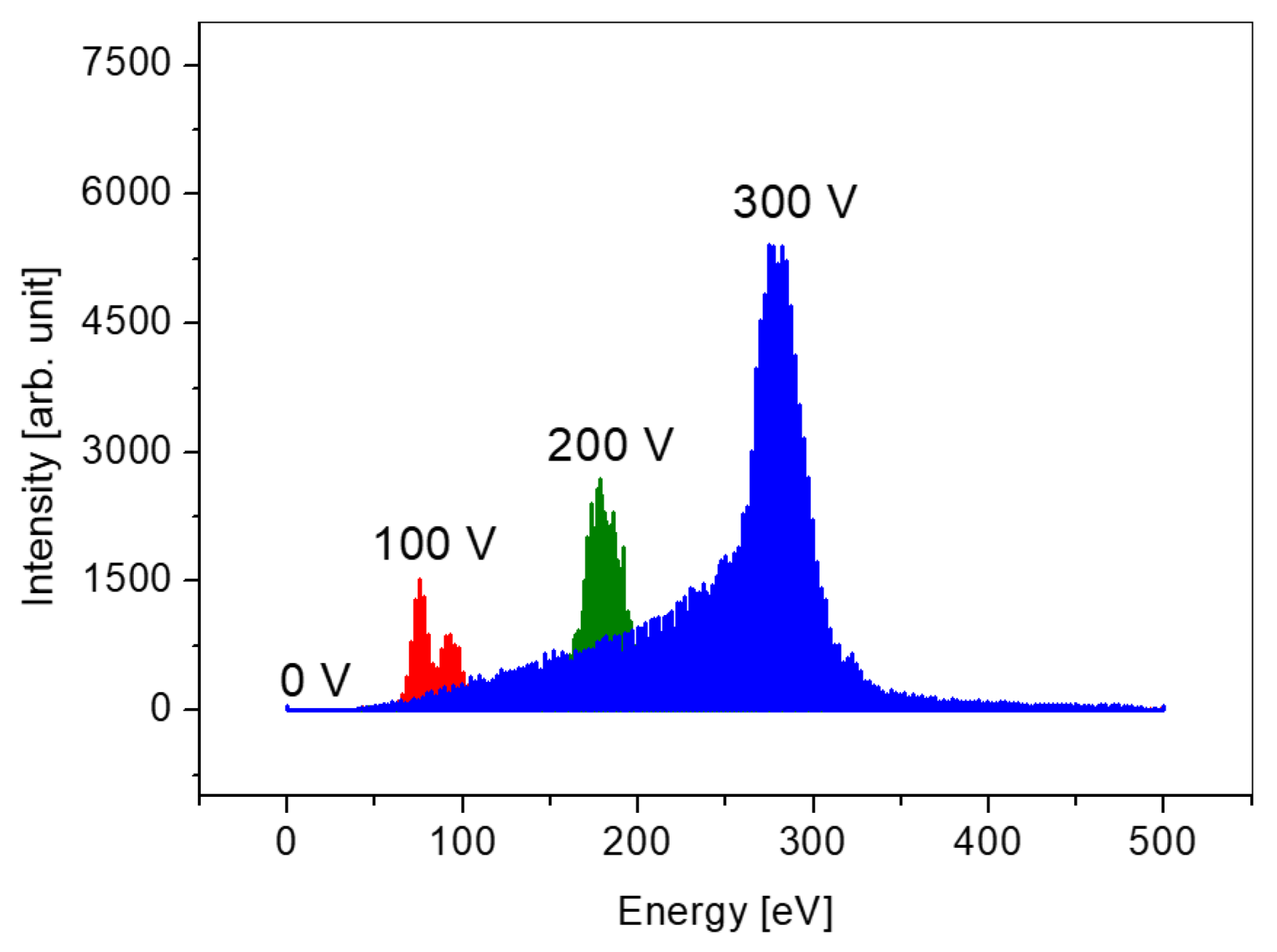
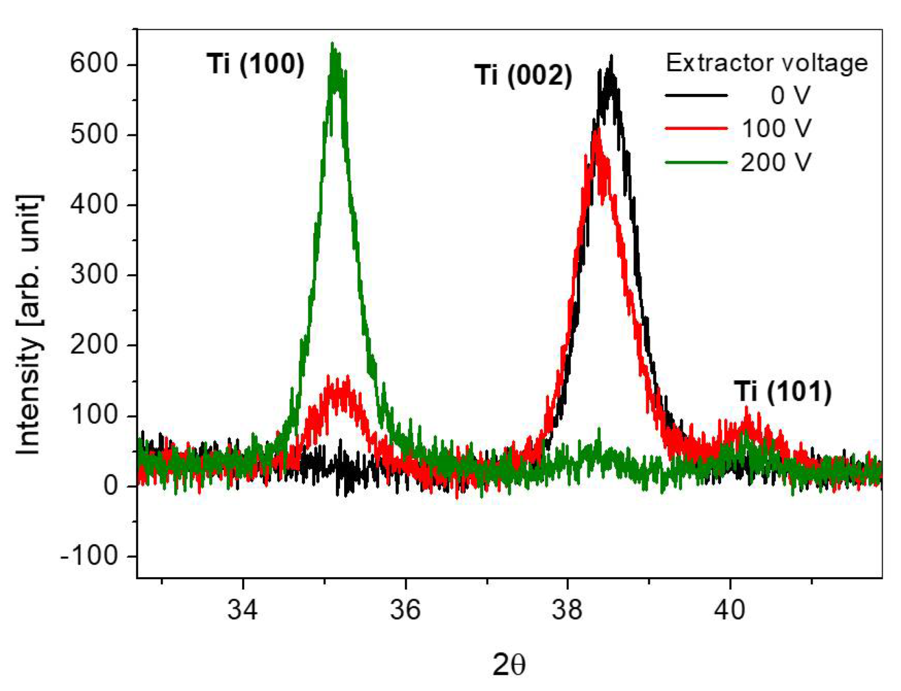
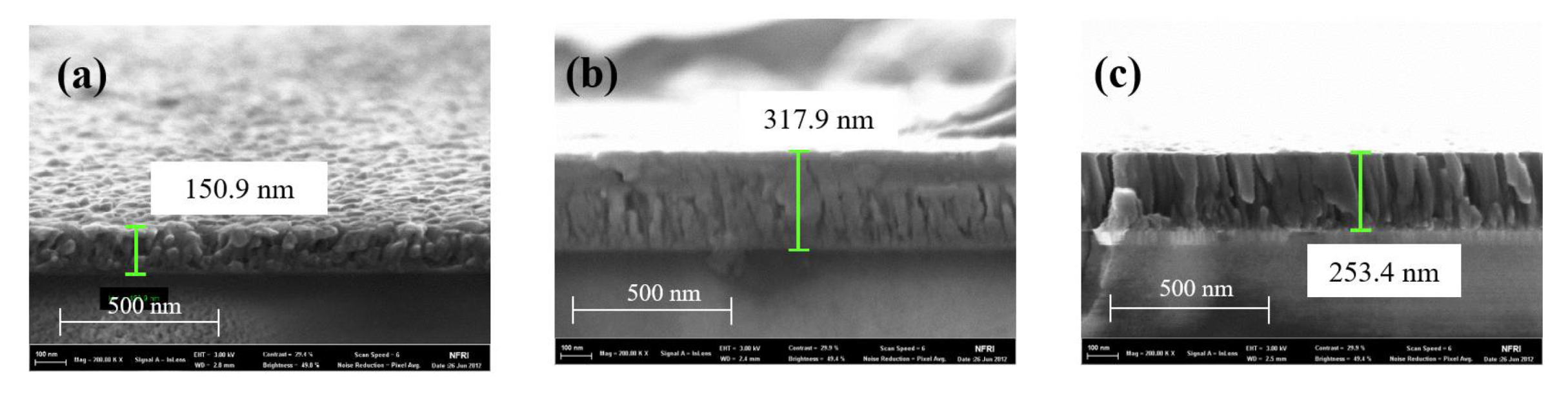
3. Results and Discussion

The target voltage and current waveforms were measured using a high-voltage probe (1000:1, P6015A, Tektronix, OR, USA) and a current probe (TCP303, TCPA300, Tektronix, OR, USA) connected to the magnetron sputter. Table 1 presents the experimental conditions. The target voltage waveforms have two steps, as illustrated in Figure 2a. During the pulse-on time of the modulator driven by an external TTL pulse, a negative voltage called the sputter voltage is applied to the sputter target to deposit the thin films on the substrate. In addition, a positive voltage is applied to the sputter target during the pulse-off time of the modulator (afterglow region), during which high-energy ions accelerate to the substrate under the extractor voltage and collide with the substrate surface, thus treating the thin films. The properties of the thin films are closely related to the variation in the extractor voltage.
Figure 2b,c shows the temporal behavior of the target current when varying the sputter voltage and extractor voltage applied to the sputter target. During the pulse-on time, the ion current increases sharply with increasing sputtering voltage. Thus, the deposition rate can be effectively increased by increasing the sputtering voltage at a constant pressure because it is directly proportional to the sputtering yield depending on the target voltage and ion flux depending on the target current. During the pulse-off time, the electron current increased with an increase in the extractor voltage compared with the pulse-on time. The plasma potential increases owing to the loss of electrons to the sputter target, thereby linearly increasing the energy of the ions reaching the substrate.
The Langmuir probe has been widely used to determine the plasma parameters because it has several advantages over other diagnostic tools. For example, it is simple, inexpensive, and reliable. The Langmuir probe, as in previous experiments [16], was used to determine the ion saturation current. The probe was biased at −40 V; therefore, we monitored the collected ion current on the oscilloscope triggered by the sputter target bias. The cylindrical probe has a tungsten tip of 0.52 mm in diameter and 3.5 mm in length and is positioned vertically 100 mm from the sputter target (substrate position). It is placed at the substrate position to estimate the relative intensity of the ions entering the substrate. Figure 3 shows the results of the ion saturation currents measured using the Langmuir probe under various extractor voltages but a fixed sputter voltage. As shown in Figure 3, the probe current increases instantaneously as the sputter voltage is applied to the sputter target and then reaches a steady state. Thereafter, when the sputter voltage was terminated, the probe current decreases rapidly. During the pulse-off time, the probe current increases slightly with an increase in the extractor voltage. In particular, the probe current varies significantly under extractor voltages greater than 300 V. When the extractor voltage is sufficiently greater than 300 V, but the sputter voltage is zero, plasma occurs near the sputter target, similar to the ion source. This result implies that the amplitude of the extractor voltage strongly affects the plasma generation and ion energy, but does not affect the target sputtering.
Figure 4 shows the IEDs for various extractor voltages. The results show that the IEDs measured by the IEA, which was placed at the substrate position, are quite similar to the extractor voltage. This means that it is possible to control the energy of the incident ion on the substrate by adjusting the extractor voltage. The intensity of the detected ion energy increases slightly with increasing extractor voltage; when the extractor voltage is >300 V, the intensity of the ion energy increases dramatically owing to the increase in the plasma density, as shown in Figure 3. The incident ions are able to transfer additional energy to the surface of the thin films during the pulse-off time. From this observation, we could control the period of the deposition and the ion treatment by adjusting the modulator parameters, such as the duty ratio and frequency. Thus, we could adjust the optimum conditions to improve the thin-film characteristics.
Through plasma treatment, organic contaminants and impurities can be removed from a sample surface via physical ablation, including energetic ion bombardment. Generally, the water contact angle is high when organic contaminants are present on a surface. Ion bombardment makes the surfaces hydrophilic, which can be observed as a decrease in the water contact angle. A clean and hydrophilic surface is important for promoting adhesion and enhancing the bond with other surfaces [17,18]. In this study, a positive voltage was applied to the sputter target in a unipolar pulse form using the modulator. Instead of wet cleaning the sample, an extractor voltage of 500 V was applied to clean the sample surface prior to deposition. Figure 5 shows the measured contact angles and subsequent hydrophobic recovery for different ion treatment times as a function of the aging time. Before the ion treatment, the initial contact angle was approximately 56°, and the value decreased below 10° when measured immediately after the ion treatment. Thereafter, the water contact angle increased gradually with increasing aging time, which implies that the glass surface became hydrophobic. This reveals that ion treatment can be used to clean a sample surface without requiring additional energy sources or substrate bias in the case of insulating surfaces, for example, glass samples.
We also observed Ti thin films deposited by ABPPS on glass, placed on the grounded substrate. Table 2 lists the experimental conditions for Ti deposition using ABPPS. Figure 6 shows the XRD patterns of the Ti thin films deposited at different extractor voltages. The (002) orientation is generally a well-known growth direction of Ti thin films when deposited on large mismatch substrates such as glass [19,20,21].
However, as shown in Figure 6, the main growth direction gradually changes from the (002) preferred orientation to the (100) orientation with an increase in the extractor voltage because additional energy is added to the Ti thin films. This implies that the ion treatment with a suitable energy strongly influences the crystal orientation of the thin films regardless of the crystallinity of the substrate. From the AFM results, we can also observe that the surface roughness of the Ti thin films deposited at extractor voltages of zero (conventional pulsed DC magnetron sputtering), 100, and 200 V has root mean square (RMS) values of 4.5, 5.3, and 2.3 nm, respectively (data are not presented herein). This shows that the thin films prepared by ion treatment with a suitable energy have a smoother surface than those prepared by conventional sputtering [22,23]. Our results are reasonably consistent with those of previous studies [19,20,21,22,23].
Figure 7 shows the cross-sectional FESEM images of Ti thin films deposited at various extractor voltages. As shown in Figure 7, the Ti thin films deposited under an extractor voltage of 200 V have a fine columnar structure and are thinner than those deposited under an extractor voltage of 100 V. This can be attributed to the increase in the ion energy supplied to the substrate, which was sufficient to suppress thin-film growth. Owing to the increase in the ion energy supplied to the substrate, the surface mobility of the adatoms increased, resulting in the formation of smooth surfaces and dense films. From the above results, the ABPPS technology was found to be effective for the surface modification of the thin films controlled by varying the extractor voltage.

4. Conclusions

We developed a cleaning and deposition method using an in-house-built ABPPS system with unipolar and bipolar pulse modes. We employed the IEA and Langmuir probe to confirm the energy distributions and relative intensity of the ions arriving at the surface of the thin films. The energy of the incident ions on the surface could be easily controlled by adjusting the amplitude of the extractor voltage. The organic contaminants on the surface could be eliminated by applying a unipolar pulse of 500 V without sputtering the Ti target. Moreover, the high-energy ions accelerated to the substrate could transfer additional energy and change the properties of the thin films during the pulse-off time. Our results confirm that the ABPPS deposition technology can be effectively used to modify the films without having to apply additional energy sources such as substrate bias or substrate heater.

Author Contributions

Conceptualization, writing and original draft preparation, D.-C.K. and Y.-H.K.; experimental work, D.-C.K. and Y.-W.K.; technical review and advising, J.-B.P., J.-S.K. and D.-S.H. All authors have read and agreed to the published version of the manuscript.

Funding

This work was supported by the National Research Council of Science & Technology (NST) grant provided by the Korean government (MSIT) (No. CRC-20-01-NFRI) and R&D Program of “Plasma BigData ICT Convergence Technology Research Project (Grant No. 1711124799)” through the Korea Institute of Fusion Energy (KFE) funded by the Government funds, Republic of Korea.

Institutional Review Board Statement

Not applicable.

Informed Consent Statement

Not applicable.

Data Availability Statement

Data are contained within the article.

Conflicts of Interest

The authors declare no conflict of interest.

References

  1. Schiller, S.; Goedicke, K.; Reschke, J.; Kirchhoff, V.; Schneider, S.; Milde, F. Pulsed magnetron sputter technology. Surf. Coat. Technol. 1993, 61, 331–337. [Google Scholar] [CrossRef]
  2. Kelly, P.J.; Arnell, R.D. Magnetron sputtering: A review of recent developments and applications. Vacuum 2000, 56, 159–172. [Google Scholar] [CrossRef]
  3. Lin, J.; Moore, J.J.; Mishra, B.; Sproul, W.D.; Rees, J.A. Examination of the pulsing phenomena in pulsed-closed field unbalanced magnetron sputtering (P-CFUBMS) of Cr–Al–N thin films. Surf. Coat. Technol. 2007, 201, 4640–4652. [Google Scholar] [CrossRef]
  4. Lin, J.; Moore, J.J.; Mishra, B.; Pinkas, M.; Sproul, W.D.; Rees, J.A. Effect of asynchronous pulsing parameters on the structure and properties of CrAlN films deposited by pulsed closed field unbalanced magnetron sputtering (P-CFUBMS). Surf. Coat. Technol. 2008, 202, 1418–1436. [Google Scholar] [CrossRef]
  5. Kelly, P.J.; Henderson, P.S.; Arnell, R.D.; Roche, G.A.; Carter, D. Reactive pulsed magnetron sputtering process for alumina films. J. Vac. Sci. Technol. A 2000, 18, 2890–2896. [Google Scholar] [CrossRef]
  6. Sellers, J. Asymmetric bipolar pulsed DC: The enabling technology for reactive PVD. Surf. Coat. Technol. 1998, 98, 1245–1250. [Google Scholar] [CrossRef]
  7. Bradley, J.W.; Bäcker, H.; Aranda-Gonzalvo, Y.; Kelly, P.J.; Arnell, R.D. The distribution of ion energies at the substrate in an asymmetric bi-polar pulsed DC magnetron discharge. Plasma Sources Sci. Technol. 2002, 11, 165–174. [Google Scholar] [CrossRef]
  8. Chun, S.Y. Asymmetric bipolar pulsed DC sputtered nanocrystalline VN coatings for electrode materials in lithium battery. J. Nanosci. Nanotechnol. 2018, 18, 1495–1498. [Google Scholar] [CrossRef] [PubMed]
  9. Zhang, L.; Shi, L.Q.; He, Z.J.; Zhang, B.; Lu, Y.F.; Liu, A.; Wang, B.Y. Deposition of dense and smooth Ti films using ECR plasma-assisted magnetron sputtering. Surf. Coat. Technol. 2009, 203, 3356–3360. [Google Scholar] [CrossRef]
  10. Hanizam; Soufhwee, H.A.R.; Anuar, K.A.R.; Nizam, A.R.M.; Mohamad, N. The effect of pulse DC and DC substrate bias during in situ cleaning PVD process on surface roughness. Procedia Eng. 2013, 53, 562–568. [Google Scholar] [CrossRef] [Green Version]
  11. Shi, Z.; Shum, P.; Zhou, Z.; Li, L.K.Y. Effect of bias voltage on the properties of CeO2−x coatings prepared by magnetron sputtering. Surf. Coat. Technol. 2017, 326, 411–416. [Google Scholar] [CrossRef]
  12. Mišina, M.; Bradley, J.W.; Bäcker, H.; Aranda-Gonzalvo, Y.; Karkari, S.K.; Forder, D. Investigation of the pulsed magnetron discharge by time- and energy-resolved mass spectrometry. Vacuum 2003, 68, 171–181. [Google Scholar] [CrossRef]
  13. Muratore, C.; Moore, J.J.; Rees, J.A. Electrostatic quadrupole plasma mass spectrometer and Langmuir probe measurements of mid-frequency pulsed DC magnetron discharges. Surf. Coat. Technol. 2003, 163–164, 12–18. [Google Scholar] [CrossRef]
  14. Barshilia, H.C.; Rajam, K.S. Reactive sputtering of hard nitride coatings using asymmetric-bipolar pulsed DC generator. Surf. Coat. Technol. 2006, 201, 1827–1835. [Google Scholar] [CrossRef]
  15. Hofer, R.R.; Haas, J.M.; Gallimore, A.D. Development of a 45-degree parallel-plate electrostatic energy analyzer for hall thruster plume studies: Preliminary Data, IEPC-99-113. In Proceedings of the 26th International Electric Propulsion Conference, Kitakyushu, Japan, 17–21 October 1999. [Google Scholar]
  16. Hopwood, J.; Guarnieri, C.R.; Whitehair, S.J.; Cuomo, J.J. Langmuir probe measurements of a radio frequency induction plasma. J. Vac. Sci. Technol. A 1993, 11, 152–156. [Google Scholar] [CrossRef]
  17. Banerjee, K.K.; Kumar, S.; Bremmell, K.E.; Griesser, H.J. Molecular-level removal of proteinaceous contamination from model surfaces and biomedical device materials by air plasma treatment. J. Hosp. Infect. 2010, 76, 234–242. [Google Scholar] [CrossRef]
  18. Terpilowski, K.; Rymuszka, D. Surface properties of glass plates activated by air, oxygen, nitrogen and argon plasma. Glass Phys. Chem. 2016, 42, 535–541. [Google Scholar] [CrossRef]
  19. Hoshi, Y.; Suzuki, E.; Shimizu, H. Control of crystal orientation of Ti thin films by sputtering. Electrochim. Acta 1999, 44, 3945–3952. [Google Scholar] [CrossRef]
  20. Jeyachandran, Y.L.; Karunagaran, B.; Narayandass, S.K.; Mangalaraj, D.; Jenkins, T.E.; Martin, P.J. Properties of titanium thin films deposited by dc magnetron sputtering. Mater. Sci. Eng. A 2006, 431, 277–284. [Google Scholar] [CrossRef]
  21. Song, Y.-H.; Cho, S.-J.; Jung, C.-K.; Bae, I.-S.; Boo, J.-H.; Kim, S. The structural and mechanical properties of Ti films fabricated by using RF magnetron sputtering. J. Korean Phys. Soc. 2007, 51, 1152–1155. [Google Scholar] [CrossRef] [Green Version]
  22. Cheng, Y.H.; Tay, B.K.; Lau, S.P.; Shi, X.; Tan, H.S. Influence of substrate bias on the microstructure and internal stress in Cu films deposited by filtered cathodic vacuum arc. J. Vac. Sci. Technol. A 2001, 19, 2102–2108. [Google Scholar] [CrossRef]
  23. Kusano, E.; Kikuchi, N. Mechanisms of the structural modification of Ti films by pulsed direct current and inductively coupled plasma-assisted pulsed direct current sputtering. Thin Solid Film. 2017, 634, 73–84. [Google Scholar] [CrossRef]
Figure 1. Schematic of the experimental device: (1) vacuum chamber; (2) vacuum pumps; (3) gas delivery system; (4) magnetron sputter; (5) modulator; (6) positive DC P/S; (7) negative DC P/S; (8) Langmuir probe; (9) oscilloscope; (10) ion energy analyzer (a pair of deflecting plates and a particle detector); (11) sample stage; (12) plasma.
Coatings 11 00904 g001
Figure 2. Target voltage and current waveforms at different sputter and extractor voltages as a function of the time. (a) Target voltage, (b) target current, and (c) high−resolution oscilloscope traces of the target current during the pulse−off time.
Coatings 11 00904 g002
Figure 3. Ion saturation currents measured using a Langmuir probe for various extractor voltages under a constant sputter voltage of −550 V as a function of time.
Coatings 11 00904 g003
Figure 4. Ion energy distributions for extractor voltages of 0, 100, 200, and 300 V under a constant sputter voltage of −550 V.
Coatings 11 00904 g004
Figure 5. Water contact angles at different ion treatment times as a function of the aging time.
Coatings 11 00904 g005
Figure 6. XRD patterns of Ti thin films deposited at extractor voltages of 0, 100, and 200 under a fixed sputter voltage of −600 V.
Coatings 11 00904 g006
Figure 7. Cross-sectional FESEM images of Ti thin films deposited at a sputter voltage of −600 V and extractor voltages of (a) 0, (b) 100, and (c) 200 V.
Coatings 11 00904 g007
Table 1. Experimental conditions.
ParameterValue
GasAr
Operating pressure (Pa)0.133
Frequency (Hz)100
Duty ratio (%)60
Sputter voltage (V)−550, −600, −650
Extractor voltage (V)0, 100, 200, 300
Table 2. Experimental conditions for Ti deposition using an asymmetric bipolar-pulsed power sputtering (ABPPS) system.
ParameterValue
Base pressure (Pa)1.33 × 10⁻⁴
GasAr
Operating pressure (Pa)0.479
Distance between target and substrate (mm)100 mm
Modulator frequency (kHz)15
Modulator duty cycle (%)60
Sputter voltage (V)(−) 600
Extractor voltage (V)0, 100, 200
SubstrateGlass
Substrate temperatureRoom temp.
Publisher’s Note: MDPI stays neutral with regard to jurisdictional claims in published maps and institutional affiliations.

