Article

Chemical Vapor Deposition of Graphene on Cu-Ni Alloys: The Impact of Carbon Solubility

1
School of Applied Sciences, University of Technology, Baghdad 964, Iraq
2
Department of Materials, The University of Manchester, Oxford Road, Manchester M13 9PL, UK
3
National Graphene Institute, Henry Royce Institute and Department of Materials, The University of Manchester, Oxford Road, Manchester M13 9PL, UK
*
Author to whom correspondence should be addressed.
Coatings 2021, 11(8), 892; https://doi.org/10.3390/coatings11080892
Submission received: 5 June 2021 / Revised: 19 July 2021 / Accepted: 20 July 2021 / Published: 26 July 2021

Abstract

:
Chemical vapour deposition (CVD) is the most promising graphene synthesis route for film and electronic applications but the growth mechanism is still not fully understood. Herein, we investigate the role of the solubility of carbon in the underlying growth substrate on the CVD growth of graphene. A range of Cu-Ni alloys compositions that cover the carbon (C) solubility range between low C solubility (pure Cu) and high C solubility (pure Ni) were used as the catalytic growth substrates. The CVD of graphene on Cu-Ni alloys showed a transition from bilayer graphene (BLG) to few-layer graphene (FLG) at a substrate Ni concentration of 45 wt.%, which was attributed to an increase in the bulk diffusion of C. The Cu-rich alloys had a high graphene coverage (BLG) at a fast-cooling rate (367 °C/min), while the Ni-rich alloys had a low coverage (FLG) under the same cooling condition. In contrast, at slow cooling rates (27 °C/min), the Cu-rich alloys had a low coverage of graphene (BLG) and the Ni-rich alloys had a high coverage of graphene (FLG). Glow discharge optical emission spectroscopy (GDOES) was used to profile the subsurface composition, particularly the C concentration, as a function of depth.

Graphical Abstract

1. Introduction

Carbon compounds make up 95% of all known chemical compounds, due to the tendency of carbon to combine with both electronegative and electropositive elements and, moreover, its ability to bond with itself in different configurations [1]. Carbon tends to hybridise in one of the following three known forms: sp, sp2 and sp3 [2]. Carbon allotropes are classified according to their dimension; (zero-dimension) 0D, (one dimension) 1D, (two-dimension) 2D and (three-dimension) 3D. Fullerenes, nanotubes, graphene and diamond are examples of the stated dimension classification, respectively [3]. Two-dimensional materials, such as graphene and graphene-like materials [4], have attracted the interest of the researchers due to their superior properties and potential applications [5,6].
Since the first successful report of graphene isolation from graphite in 2004 [7], several methods have been developed for graphene synthesis. All of these methods may be categorised as either top-down or bottom-up. For the top-down approach, bulk graphite is isolated into individual two-dimension graphene sheets through chemical exfoliation, mechanical cleavage etc., whilst the bottom-up approaches form graphene sheets from their constituent building blocks (atoms or molecules), typically on a supporting substrate, as in the CVD method. The first attempt to grow graphene using CVD was reported by Somani and co-workers in 2006 [8] using camphor (C10H16O) as a C source and Ni foil as the hot substrate. The process resulted in few-layer graphene (FLG) growth with an interlayer spacing of 0.34 nm. Even though the graphitic film was very thick, their work highlighted the possibility of graphene synthesis using CVD.
The breakthrough was made by Ruoff et al., who reported the CVD of single-layer graphene (SLG) on a Cu substrate [9]. A 25-micrometer-thick Cu foil was annealed in a hydrogen atmosphere at 1000 °C, followed by methane (CH4) at low pressure. The resulting deposited film was ~95% SLG with a small percentage of FLG. The graphene film was found to be continuous over the Cu grain boundaries and steps. Byung et al. demonstrated the ability of CVD to produce graphene films across areas as wide as 30 inches with a 95% SLG coverage. This work demonstrated that CVD can meet the demands of thin film applications in terms of quality and scalability.
Nevertheless, there are remaining challenges for the CVD of graphene, including controlling the number of layers and grain size, for which further study of the CVD graphene growth mechanism is needed. The CVD growth of graphene is a surface reaction process; the metal surface is exposed to a hydrocarbon, usually CH4, which leads to stepwise dehydrogenation and liberation of C [10]. Based upon C isotope labelling, the CVD graphene growth mechanism is believed to be via the surface adsorption of carbon species for metals with low C solubility (e.g., Cu) [11]. In this process, C diffuses on the substrate surface until its concentration increases, reaches a critical supersaturation level and graphene nucleation takes place. Thus, graphene growth is completely controlled by a vapor–surface reaction that is commonly a self-limited growth process [12]. In contrast, for high C solubility metals, growth occurs by the segregation of C from saturated substrates (e.g., Ni). In this process, the C active species initially diffuse into the substrate bulk and when the C concentration reaches close to the C solubility limit (e.g., by a change of temperature), graphene nucleation occurs by a precipitation–segregation process [10,13,14,15]. Even though the CVD growth of single-layer graphene is self-limiting on Cu, achieving a large single crystal and controlling the number of graphene layers is challenging [11]. On the other hand, using a Ni substrate results in inhomogeneous graphitic films with varying thicknesses because of the Ni’s high C solubility [16].
Both theoretical studies and experimental results have found that alloying Ni with Cu decreases the C solubility in the Cu-Ni system [17]. Combining the high catalytic activity of Ni with the low C solubility of Cu is a promising route to control a number of layers of graphene during film growth. Xie et al. reported the growth of 300-micrometer domain size AB-stacked BLG with the Cu vapour assistance on 25-micrometer-thick electrodeposited Cu85-Ni15 alloy [18]. Liu and co-workers achieved 95% SLG graphene coverage on a 300-nanometer Cu94.5-Ni5.5 film substrate; however, by increasing the Ni content to 10.4%, the produced graphene was 89% BLG [19]. Ruoff et al. have investigated the CVD of graphene on commercial Cu31-Ni67.8 [20] and Cu90-Ni10 [21] alloys; they found that the thickness of precipitated graphene is influenced by both the growth temperature and the cooling rate. A Cu-Ni alloy thin film has been previously used to synthesise graphene; Jeon et al. found that the number of graphene layers can be controlled by controlling the Ni content in the Cu-Ni thin film [22]. Prior studies using Cu-Ni alloys as a catalytic substrate for CVD graphene are limited both in number and the composition range studied [13,19,20,21,22,23,24,25,26,27,28,29]; therefore, further study is required.
Hence, herein, we use a range of Cu-Ni alloys to investigate how growth transitions between the two mechanisms (surface reaction and segregation). In particular, a transition between low and high C solubility on the CVD growth mechanism is seen at a Ni concentration of 45 wt.%.

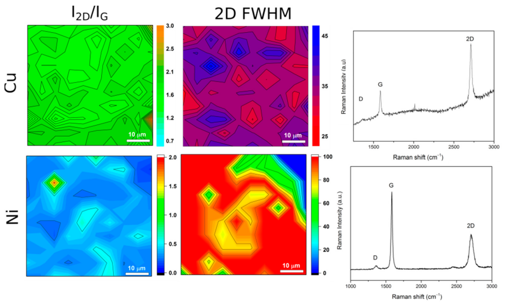
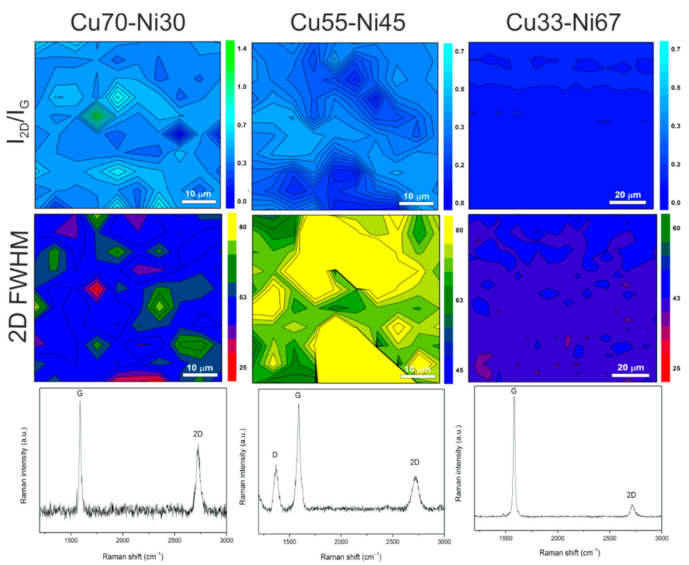
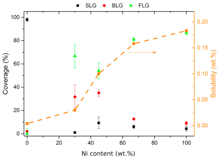
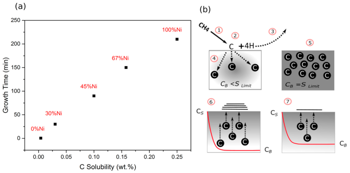
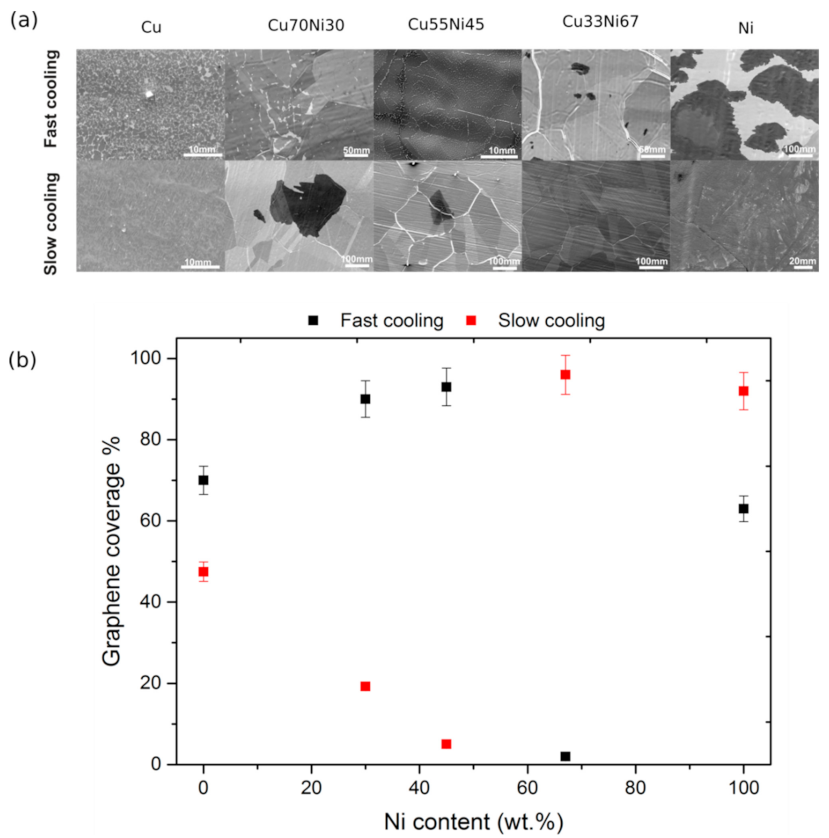
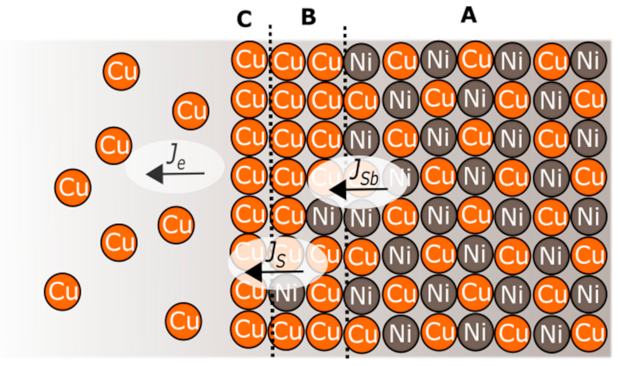
2. Results and Discussion

CVD growth was initially conducted on pure metals substrate (Cu and Ni) with a thickness of 500 µm. Raman spectra were collected from the result films (Figure 1). The graphene grown on the Cu has an I2D/IG ratio of ~1.8 and a 2D FWHM of 30, which is in good agreement with the reported Raman fingerprint for CVD single-layer graphene [9]. However, the I2D/IG of the graphene grown on the Ni is ~0.5, which indicates a thicker graphitic film formed on the surface [11,30].
CVD was then conducted under the same conditions on Cu-Ni alloys with compositions of Cu70-Ni30, Cu55, Ni45 and Cu33-Ni67, by weight ratio. Figure 2 shows the Raman spectra and maps obtained from the resulting graphene films. It can be seen that the Raman spectra transitioned from being similar to that found on pure Cu to that found on pure Ni with increasing Ni content within the alloy. These maps were used to calculate the arial coverage of SLG, BLG and FLG (Figure 3). The 100 wt.% Cu substrate was found to be virtually covered by pure SLG. The degree of BLG and FLG content was found to increase with the Ni content, such that the films were almost entirely FLG on 100% Ni. The reported C solubility [17] of the corresponding alloys is also plotted in Figure 3 to aid understanding of the results. (For reference, the Raman maps for samples grown at lower pressures are in given in Figure S1).
The increasing thickness of the graphene with increasing Ni content correlates with the increase in C solubility with higher Ni content. Furthermore, introducing Ni not only increased the C solubility but also increased the alloy’s catalytic activity towards hydrocarbon decomposition [31,32]. The C solubility of the growth substrate should also effect the growth time of the graphene. Figure 4a plots the time required to grow a graphene (e.g., SLG, BLG or FLG) film against Ni content and compares it with each alloy’s C solubility values. As can be seen, the growth time increases with the increasing C solubility of the Cu-Ni alloy. This observation is consistent with the CVD graphene growth on the Cu-Ni alloy being a bulk diffusion–precipitation process. When the hydrocarbon (CH4) interacts with the metal surface, C atoms are liberated through breaking the C–H bond (Figure 4b) and diffuse into the metal bulk. The C concentration in the metal bulk (CB) increases up to the solubility limit (SLimit) for a given substrate [10]. When the precursor supply is stopped and the substrate is cooled, the growth of the graphene occurs through C precipitation at the surface [33,34]. The incubation period (the required time to fulfil the CB ≈ SLimit condition) is dependent on the growth parameters (temperature, pressure and feeding stock composition) and C solubility.
The cooling rate plays a critical role in controlling the amount of solute C in the diffusion–precipitation process. The SEM images for the CVD graphene grown under the same conditions, but with different cooling rates, show a diverse range in the surface coverage (Figure 5a). The graphene surface coverage percentage was determined by using Image J (Java-based image processing programme, 1.52n) and is plotted in Figure 5b. Under fast cooling conditions, the graphene film shows a transition from high coverage with the Cu-rich alloy to low coverage with the Ni-rich alloy. However, during slow cooling conditions, the behaviour reversed, with low graphene coverage on the Cu-rich alloy and more coverage with the Ni-rich alloys. CVD graphene coverage on pure metals (Cu and Ni) is also affected by the cooling rate; however, the difference between slow and fast cooling rates is not marked. In order to determine the reasons for this transition in behaviour with cooling rate, it is necessary to ascertain the composition of the alloy (Cu, Ni and C content) beneath the surface on which the graphene film is grown.
Glow discharge optical emission spectroscopy (GDOES) was used to perform concentration–depth profile analysis to explicate the results in Figure 5. The concentration of the selected element is proportional to the measured emission intensities, which expressed in Equation (1) [35], as follows:
I λ E = α λ E C E , M
where I λ E , M is the intensity of the emission line of element E, C E , M is the concentration of the element and α λ E is a constant.
The bulk C depth profile of the pure Cu shows no difference between the slow and fast cooling rates. However, the C profile shows a higher C concentration at the surface and a gradual decrease in the subsurface (Figure 6).
In contrast, the C depth profile of the slow and fast cooled pure Ni samples shows three distinct regions (I, II and III), which are assigned, respectively, to the surface, subsurface and bulk (Figure 6). The slow cooling rate of the substrate from 1000 °C to room temperature drove more C atoms to diffuse towards the surface, which is evident from the depth profile of the region I compared with the fast cooling rate sample. Region II is characterised by an increasing Ni intensity with depth until it reaches the bulk value. Moreover, the subsurface region is a C-rich, Ni–C solid solution, which feeds the graphitic film on the surface during the cooling stage [36]. At fast cooling rates, the subsurface thickness is about five times smaller than slow cooling, explaining the variation in graphitic film thickness on the surface.
Figure 7 shows the depth–intensity profile of the three elements, Cu, Ni and C, in the Cu-Ni alloys. There is a clear difference in the depth profiles with different cooling rates. The profiles for all of the alloys under fast cooling show a stable and smooth plasma intensity for both Cu and Ni, except near the substrate surface, where the intensity increases due to the influence of the free surface [37]. However, the depth profiles for the slow cooling rate alloy show a change in the intensity. For the Cu70-Ni30 alloy, at a depth of 2.18 µm (0.07 µm below the surface), the Cu intensity decreases, and the Ni intensity increases significantly. However, at a 0.6 µm depth, the Cu and Ni intensities are constant. The variation in the Cu and Ni intensity profile diminishes when the proportion of Ni increases in the alloy. For example, the change in the Ni depth profile below the Cu55-Ni45 surface is very minimal compared to that in seen in the Cu70-Ni30 alloy and the variation is absent in the Ni-rich alloy.
The Ni and Cu plasma intensity change near the Ni-rich substrate surface is minimal at a slow cooling rate. The GDOES results for the Cu-Ni alloys can be summarised as follows:
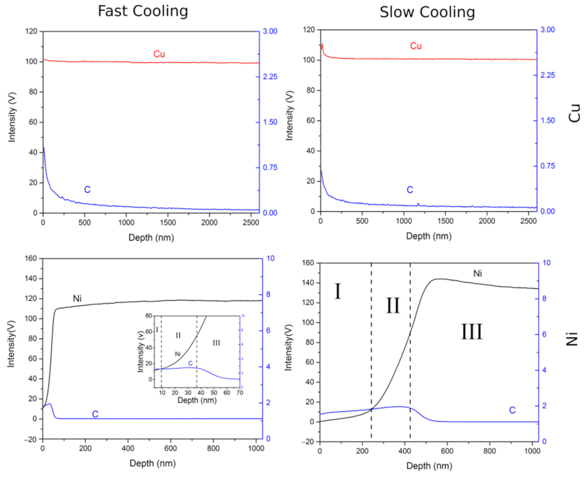
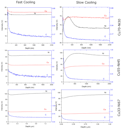
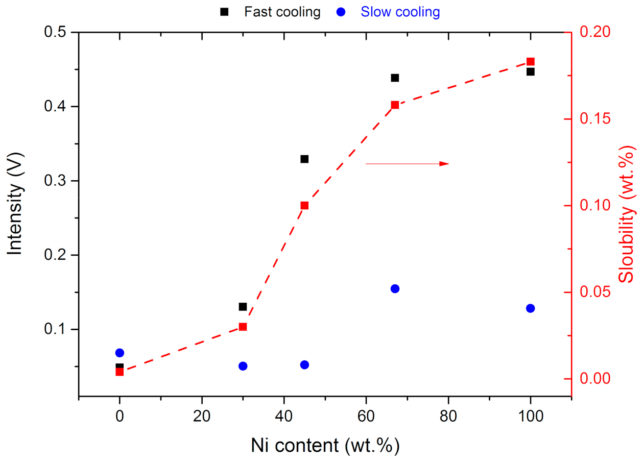
  • The plasma intensity of Cu and Ni at the surface is always higher than the bulk (the flat intensity region), regardless of the cooling rate.
  • After fast cooling rates, the plasma intensity profile is smooth and flat for both the Cu and Ni signal.
  • The slowly cooled samples exhibit disturbances in Cu and Ni intensity at the surface and subsurface, indicating a local change in the alloy composition.
  • The intensity (composition) changes with the Ni content are more evident for the Cu70–Ni30 substrate alloy than for Cu33-Ni67.
The gradual increase in GDOES intensity near the surface for both Cu and Ni has been reported previously for Cu-Ni alloys. It is believed to be due to a change in the Cu-Ni composition close to the free surface [37,38]. There is a difference in the surface and bulk composition of the Cu-Ni alloy studied experimentally and theoretically. The results confirm that the Cu-Ni alloy surface is always Cu-rich [39,40,41]. Furthermore, the concentration of Cu at the alloy surface is influenced by both the working temperature and the bulk alloy concentration [41].
The low-pressure and high temperature conditions during the annealing and growth period facilitates Cu evaporation from the alloy surface due to the proximity of the working temperature to Cu’s melting temperature (1084 °C). Thus, to explain the GDOES results in Figure 7 satisfactorily, one needs to consider the Lea and Seah kinetic model for surface segregation in the case of evaporation in an alloy system [42]. The model takes into consideration the competing mechanisms between evaporation from the surface (Je), bulk to subsurface diffusion (JSb) and subsurface to surface diffusion (JS) as a function of temperature [43] (Figure 8). Webber and Chadwick established the following simple expression following Lea and Seah’s work to describe the evaporation of Cu in Cu-Ni alloy [44]:
C S t C S = exp 1 E D t α 2 d 2 1 exp E D t α 2 d 2 erf D t α 2 d 2 1 2
where C S t is the Cu concentration at the surface at time t and C S is the Cu surface concentration when evaporation is zero, α is the enrichment ratio (concentration of Cu on the surface ( C S t ) to the subsurface concentration ( C 0 t )), D is the diffusion coefficient, d is the surface layer thickness and E is a dimensionless parameter to describe the evaporation rate such that [44]:
E v a p o r a t i o n   r a t e = 10 4 C 0 t E D α 2 d 2
This equation assumes that the Cu is distributed evenly in the substrate, and the surface, subsurface and bulk concentrations are equal, and the fluxes are zero (Je = JS = Jsb = 0). When the temperature is increased, the Cu concentration on the surface increases as a result of subsurface to surface segregation. This deficiency in the subsurface concentration is overcome by the diffusion of Cu from the bulk region. At this point JS and Jsb ≠ 0; however, the evaporation flux is still zero (Je = 0) until the surface concentration is sufficiently high to reach a Cu vapour pressure higher than ambient pressure (0.11 mbr). At this point, Cu begins to evaporate (E > 0). The evaporation rate reaches its maximum value at 1000 °C (E = 1); consequently, the Cu surface concentration decreases. The system retains the equilibrium by Cu diffusing from the bulk to the depleted Cu region at the subsurface, which feeds the surface.
Consequently, when the growth terminates and the sample cools down at a fast cooling rate (~376 °C/min), the three fluxes (Je, JS and Jsb) reach their minimum values in a short time, resulting in a constant GDOES depth profile for all three Cu-Ni samples, reflecting the composition homogeneity during the growth period.
When the Cu evaporation rate reduces from the alloy surface (E → 0), its surface concentration increases to the maximum. That increase comes from the diffusion of Cu from below the surface to the surface. This process is irreversible, resulting in Cu consumption below the surface. Inhomogeneity at the surface and subsurface regions creates diversity in the C solubility values, i.e., the Cu-rich surface has a lower SLimit than the Ni-rich subsurface region, which consequently impacts the graphene coverage. Based on Equation (2), the surface concentration is related primarily to the initial alloy composition. Therefore, the impact of evaporation–diffusion segregation is higher for the Cu-rich alloys (Cu70-Ni30 and Cu55-Ni45) than the Ni-rich alloy (Cu33-Ni67).
The C depth profile for all the Cu-Ni alloys in this study shows a higher bulk intensity of C at fast cooling rates than at a slow cooling rate (Figure S2). This result might be due to the short C segregation time during the cooling rate. Moreover, there is an increase in the intensity of the C signal when the Ni content increases.
To further understand the relationship between the incubation time and the C content in the substrate, the C intensity at the deepest measured point (which is assumed to represent the bulk) is plotted against the Ni content for both a fast and slow cooling rate (Figure 9). It is clear that both the fast and slow cooled samples have the same trend as the reported C solubility for the alloy under study. Moreover, the difference in C intensity is considerable between the fast and slow cooled samples. The data shown in Figure 9 agrees with the proposed diffusion–perspiration mechanism for Cu-Ni alloy substrates. The C solubility limit in the alloys represents the amount of C that diffuses into the substrate during the incubation period. When the maximum solubility concentration is achieved, the growth of graphene on the surface is possible. If the sample cooled down quickly, then the amount of C that can diffuse back to the surface is small; however, at the slow cooling rate, the substrate remains at an elevated temperature for enough time to allow C to diffuse toward the surface (which explains why Cu33-Ni67 has a high graphene coverage). The difference in composition between the surface, subsurface and the bulk of a Cu-Ni alloy leads to a change in C solubility and diffusivity within the same substrate. Consequently, a diffusion barrier might develop, preventing carbon segregation from the bulk towards the surface under some conditions, possibly explaining the low graphene coverage observed at the slow cooling rate for Cu70-Ni30 and Cu55-Ni45 substrates.

3. Conclusions

In conclusion, the CVD of graphene was performed on Cu-Ni alloys and the resulting films were characterised. Single-layer graphene was dominant in the films grown on the Cu substrates, whereas few-layer graphene grew on the Ni substrate. The thickness of the films grown on the Cu-Ni alloy was closely related to the Ni content in the alloy. By increasing the Ni content, the percentage of FLG coverage increased, reaching full FLG coverage for pure Ni substrates. This result was attributed to the rise in C solubility with an increasing Ni content. The substrate surface coverage was highly affected by the sample cooling rate after growth; Cu-rich substrates require fast cooling to achieve good surface coverage, while a slow cooling rate is needed for Ni-rich substrates to gain good surface coverage. The GDOES results revealed that the subsurface region of the Cu-rich alloy substrates was actually Ni-rich due to Cu evaporation. This Ni region may have acted as a diffusion barrier, preventing C precipitation to the surface. The depth profile of the C intensity was found to depend on the Ni concentration, reflecting the change in C solubility behaviour.

4. Methods

4.1. Graphene Growth

A hot-wall CVD system that was built in-house was used to grow the graphene samples. The system comprised a tube furnace (Lenton Eurotherm, Worthin, UK) and a 1-inch outer diameter quartz tube as the growth chamber. Low pressure was achieved using a rotary vane pump (Edwards RV12, Edwards Vacuum, Burgess Hill, UK) with a capacitance manometer gauge (Leybold Oerlikon CTR100, Leybold GmbH, Kölner, Germany) to monitor it. The growth procedure is illustrated in Figure S3; a small piece of the 500-micrometer-thick Cu-Ni alloys (substrates supplier, composition and purity shown in Table S1) was placed in the centre of the furnace isothermal zone. The substrate is first annealed under a flow of hydrogen (99.95%, BOC, Guilford, UK) at 1000 °C for 20 min at a base pressure of 0.035 mbar. Growth was then started by flowing methane (99.95%, BOC, Guilford, UK) into the chamber at a growth pressure of 0.11 mbar for a specific time for each Cu-Ni composition; subsequently, the sample was cooled down under the hydrogen flow either slowly (27 °C/min) or quickly (376 °C/min).

4.2. Sample Characterisation

All the graphene films were characterised whilst on the growth substrate. The scanning electron microscopy (SEM) images were acquired using an XL-30 FEG SEM (FEI, Eindhoven, The Netherlands) at an accelerating voltage of 8 kV. A LabRAM HR Evolution Raman system (Jobin Yvon, Kyoto, Japan) with a 488-nanometer wavelength laser was used to characterise graphene coverage and uniformity. For the mapping, the range was set for I2D/IG from 1.4 to 0.7 and 2D FWHM from 45 to 60 cm−1 for BLG: an I2D/IG ratio higher than 1.4 and a FWHM of 2D peak less than 45 cm−1, indicated SLG, while an I2D/IG ratio less than 0.7 and a 2D peak FWHM of 60 cm−1 indicated FLG [45,46]. A GDOES depth profiler (HORIBA Jobin Yvon, Kyoto, Japan) was used for the depth profile of the Cu, Ni and C profile in substrate bulk. Both the argon flash time and sputtering time was 30 s and the emission lines for Cu, Ni and C were 325, 341 and 156 nm, respectively.

4.3. Experiment Parameters

Raman I2D/IG and 2D band FWHM maps for 25 µm Cu. Distribution of graphene coverage vs. copper substrate thickness. Raman maps of CVD graphene grow on Cu-Ni alloy at growth pressure 0.65 mbar. SEM images of Cu, Ni and Cu-Ni substrates at a slow and fast cooling rate. GDOES C intensity against sputtering time in the Cu-Ni alloys. Experimental procedure of CVD growth process. Substrate specifications.

Supplementary Materials

The following are available online at https://www.mdpi.com/article/10.3390/coatings11080892/s1, Figure S1: Raman I2D/IG and 2D band FWHM Cu-Ni alloys. Growth conditions were 1000 °C growth temperature, 0.65 mbar growth pressure, and fast cooling rate, Figure S2: GDOES C intensity vs. sputtering time profile in Cu-Ni alloys. Growth conditions are 1000 °C growth temperature, 0.1 mbar growth pressure, fast cooling rate and growth time as stated in Figure 5, Figure S3: Schematic illustrating the experimental pro-cedure used for the CVD growth process, Table S1: Substrate specifications used in this work.

Author Contributions

Data curation, S.H.A.-H.; Formal analysis, S.H.A.-H.; Methodology, S.H.A.-H.; Supervision, I.A.K. and B.D.; Visualization, S.H.A.-H.; Writing—original draft, S.H.A.-H.; Writing—review & editing, I.A.K. All authors have read and agreed to the published version of the manuscript.

Funding

This research received no external funding.

Institutional Review Board Statement

Not applicable.

Informed Consent Statement

Not applicable.

Data Availability Statement

All research data supporting this publication are available within this publication.

Acknowledgments

Special thanks to the Iraqi government and the University of Technology-Baghdad for their financial support. IAK acknowledges the EPSRC (EP/I023879/1) and the Royal Academy of Engineering and Morgan Advanced Materials for his Chair. Thanks to Andrew Wallwork for his technical assistance regarding the maintenance of the CVD reactor. The authors wish to extend our special thanks to Ben F. Spencer for his assistance with the GDOES measurements.

Conflicts of Interest

The authors declare no conflict of interest.

References

  1. Falcao, E.H.L.; Wudl, F. Carbon allotropes: Beyond graphite and diamond. J. Chem. Technol. Biotechnol. 2007, 82, 524–531. [Google Scholar] [CrossRef]
  2. Inagaki, M.; Kang, F. Graphene derivatives: Graphane, fluorographene, graphene oxide, graphyne and graphdiyne. J. Mater. Chem. A 2014, 2, 13193–13206. [Google Scholar] [CrossRef]
  3. Georgakilas, V.; Perman, J.A.; Tucek, J.; Zboril, R. Broad family of carbon nanoallotropes: Classification, chemistry, and applications of fullerenes, carbon dots, nanotubes, graphene, nanodiamonds, and combined superstructures. Chem. Rev. 2015, 115, 4744–4822. [Google Scholar] [CrossRef]
  4. Yang, D.-C.; Jia, R.; Wang, Y.; Kong, C.-P.; Wang, J.; Ma, Y.; Eglitis, R.I.; Zhang, H.-X. Novel carbon nanotubes rolled from 6,6,12-graphyne: Double dirac points in 1d material. J. Phys. Chem. C 2017, 121, 14835–14844. [Google Scholar] [CrossRef]
  5. Huang, H.; Shi, H.; Das, P.; Qin, J.; Li, Y.; Wang, X.; Su, F.; Wen, P.; Li, S.; Lu, P.; et al. The chemistry and promising applications of graphene and porous graphene materials. Adv. Funct. Mater. 2020, 30, 1909035. [Google Scholar] [CrossRef]
  6. Liu, Y.; Zheng, J.; Zhang, X.; Li, K.; Du, Y.; Yu, G.; Jia, Y.; Zhang, Y. Recent advances on graphene microstructure engineering for propellant-related applications. J. Appl. Polym. Sci. 2021, 138, 50474. [Google Scholar] [CrossRef]
  7. Novoselov, K.S.; Geim, A.K.; Morozov, S.V.; Jiang, D.; Zhang, Y.; Dubonos, S.V.; Grigorieva, I.V.; Firsov, A.A. Electric field effect in atomically thin carbon films. Science 2004, 306, 666–669. [Google Scholar] [CrossRef] [Green Version]
  8. Somani, P.R.; Somani, S.P.; Umeno, M. Planer nano-graphenes from camphor by CVD. Chem. Phys. Lett. 2006, 430, 56–59. [Google Scholar] [CrossRef]
  9. Li, X.; Cai, W.; An, J.; Kim, S.; Nah, J.; Yang, D.; Piner, R.; Velamakanni, A.; Jung, I.; Tutuc, E.; et al. Large-area synthesis of high-quality and uniform graphene films on copper foils. Science 2009, 324, 1312–1314. [Google Scholar] [CrossRef] [Green Version]
  10. Al-Hilfi, S.H.; Derby, B.; Martin, P.A.; Whitehead, J.C. Chemical vapour deposition of graphene on copper–nickel alloys: The simulation of a thermodynamic and kinetic approach. Nanoscale 2020, 12, 15283–15294. [Google Scholar] [CrossRef]
  11. Li, X.; Cai, W.; Colombo, L.; Ruoff, R.S. Evolution of graphene growth on Ni and Cu by carbon isotope labeling. Nano Lett. 2009, 9, 4268–4272. [Google Scholar] [CrossRef] [Green Version]
  12. Zhang, J.; Lin, L.; Jia, K.; Sun, L.; Peng, H.; Liu, Z. Controlled growth of single-Crystal graphene films. Adv. Mater. 2020, 32, 1903266. [Google Scholar] [CrossRef] [Green Version]
  13. Huang, M.; Ruoff, R.S. Growth of single-layer and multilayer graphene on Cu/Ni alloy substrates. Acc. Chem. Res. 2020, 53, 800–811. [Google Scholar] [CrossRef]
  14. Uddin, S.; Song, Y.-W. Directly synthesized graphene-based photonics and optoelectronics devices. Appl. Sci. 2021, 11, 2768. [Google Scholar] [CrossRef]
  15. Fazi, A.; Nylander, A.; Zehri, A.; Sun, J.; Malmberg, P.; Ye, L.; Liu, J.; Fu, Y. Multiple growth of graphene from a pre-dissolved carbon source. Nanotechnology 2020, 31, 345601. [Google Scholar] [CrossRef] [PubMed]
  16. Reina, A.; Jia, X.; Ho, J.; Nezich, D.; Son, H.; Bulovic, V.; Dresselhaus, M.S.; Jing, K. Large area, few-layer graphene films on arbitrary substrates by chemical vapor deposition. Nano Lett. 2009, 9, 30–35. [Google Scholar] [CrossRef]
  17. Nicholson, M.E. The solubility of carbon in nickel-copper alloys at 1000 °C. Transcation Metall. Soc. AIME 1962, 224, 533. [Google Scholar]
  18. Yang, C.; Wu, T.; Wang, H.; Zhang, G.; Sun, J.; Lu, G.; Niu, T.; Li, A.; Xie, X.; Jiang, M. Copper-vapor-assisted rapid synthesis of large AB-stacked bilayer graphene domains on Cu-Ni Alloy. Small 2016, 12, 2009–2013. [Google Scholar] [CrossRef]
  19. Liu, X.; Fu, L.; Liu, N.; Gao, T.; Zhang, Y.; Liao, L.; Liu, Z. Segregation growth of graphene on Cu-Ni alloy for precise layer control. J. Phys. Chem. C 2011, 115, 11976–11982. [Google Scholar] [CrossRef]
  20. Chen, S.; Cai, W.; Piner, R.D.; Suk, J.W.; Wu, Y.; Ren, Y.; Kang, J.; Ruoff, R.S. Synthesis and characterization of large-area graphene and graphite films on commercial Cu-Ni alloy foils. Nano Lett. 2011, 11, 3519–3525. [Google Scholar] [CrossRef]
  21. Wu, Y.; Chou, H.; Ji, H.; Wu, Q.; Chen, S.; Jiang, W.; Hao, Y.; Kang, J.; Ren, Y.; Piner, R.D.; et al. Growth mechanism and controlled synthesis of AB-stacked bilayer graphene on Cu-Ni alloy foils. ACS Nano 2012, 6, 7731–7738. [Google Scholar] [CrossRef]
  22. Choi, H.; Lim, Y.; Park, M.; Lee, S.; Kang, Y.; Kim, M.S.; Kim, J.; Jeon, M. Precise control of chemical vapor deposition graphene layer thickness using NixCu1−x alloys. J. Mater. Chem. C 2015, 3, 1463–1467. [Google Scholar] [CrossRef]
  23. Madito, M.J.; Manyala, N.; Bello, A.; Dangbegnon, J.K.; Masikhwa, T.M.; Momodu, D.Y. A wafer-scale Bernal-stacked bilayer graphene film obtained on a dilute Cu (0.61 at.% Ni) foil using atmospheric pressure chemical vapour deposition. RSC Adv. 2016, 6, 28370–28378. [Google Scholar] [CrossRef] [Green Version]
  24. Robinson, Z.R.; Tyagi, P.; Murray, T.M.; Ventrice, C.A., Jr.; Chen, S.; Munson, A.; Magnuson, C.W.; Ruoff, R.S. Substrate grain size and orientation of Cu and Cu–Ni foils used for the growth of graphene films. J. Vac. Sci. Technol. A 2012, 30, 011401. [Google Scholar] [CrossRef] [Green Version]
  25. Lee, W.G.; Kim, E.; Jung, J. Fast and simultaneous growth of graphene, intermetallic compounds, and silicate on Cu-Ni alloy foils. Mater. Chem. Phys. 2014, 147, 452–460. [Google Scholar] [CrossRef]
  26. Wu, T.; Liu, Z.; Chen, G.; Dai, D.; Sun, H.; Dai, W.; Jiang, N.; Jiang, Y.H.; Lin, C.-T. A study of the growth-time effect on graphene layer number based on a Cu-Ni bilayer catalyst system. RSC Adv. 2016, 6, 23956–23960. [Google Scholar] [CrossRef]
  27. Tyagi, P.; Robinson, Z.R.; Munson, A.; Magnuson, C.W.; Chen, S.; McNeilan, J.D.; Moore, R.L.; Piner, R.D.; Ruoff, R.S.; Ventrice, C.A. Characterization of graphene films grown on CuNi foil substrates. Surf. Sci. 2015, 634, 16–24. [Google Scholar] [CrossRef]
  28. Zhang, X.; Wu, T.; Jiang, Q.; Wang, H.; Zhu, H.; Chen, Z.; Jiang, R.; Niu, T.; Li, Z.; Zhang, Y.; et al. Epitaxial Growth of 6 in. Single-Crystalline Graphene on a Cu/Ni (111) Film at 750 °C via Chemical Vapor Deposition. Small 2019, 15, 1805395. [Google Scholar] [CrossRef]
  29. Wu, T.; Zhang, X.; Yuan, Q.; Xue, J.; Lu, G.; Liu, Z.; Wang, H.; Wang, H.; Ding, F.; Yu, Q.; et al. Fast growth of inch-sized single-crystalline graphene from a controlled single nucleus on Cu–Ni alloys. Nat. Mater. 2015, 15, 43–47. [Google Scholar] [CrossRef]
  30. Ferrari, A.C. Raman spectroscopy of graphene and graphite: Disorder, electron–phonon coupling, doping and nonadiabatic effects. Solid State Commun. 2007, 143, 47–57. [Google Scholar] [CrossRef]
  31. Bernardo, C.A.; Alstrup, I.; Rostrup-Nielsen, J.R. Carbon deposition and methane steam reforming on silica-supported NiCu catalysts. J. Catal. 1985, 96, 517–534. [Google Scholar] [CrossRef]
  32. Reynolds, P.W. 57. Heterogeneous catalysis. Part II. Hydrogenation by binary alloys. J. Chem. Soc. 1950, 265–271. [Google Scholar] [CrossRef]
  33. Weatherup, R.S.; Bayer, B.C.; Blume, R.; Ducati, C.; Baehtz, C.; Schlögl, R.; Hofmann, S. In situ characterization of alloy catalysts for low-temperature graphene growth. Nano Lett. 2011, 11, 4154–4160. [Google Scholar] [CrossRef]
  34. Snoeck, J.-W.; Froment, G.F.; Fowles, M. Filamentous carbon formation and gasification: Thermodynamics, driving force, nucleation, and steady-state growth. J. Catal. 1997, 169, 240–249. [Google Scholar] [CrossRef]
  35. Weiss, Z. Calibration methods in glow discharge optical emission spectroscopy: A tutorial review. J. Anal. At. Spectrom. 2015, 30, 1038–1049. [Google Scholar] [CrossRef]
  36. Weatherup, R.S.; Amara, H.; Blume, R.; Dlubak, B.; Bayer, B.C.; Diarra, M.; Bahri, M.; Cabrero-Vilatela, A.; Caneva, S.; Kidambi, P.R.; et al. Interdependency of subsurface carbon distribution and graphene-catalyst interaction. J. Am. Chem. Soc. 2014, 136, 13698–13708. [Google Scholar] [CrossRef]
  37. Wagatsuma, K.; Hirokawa, K. Analysis of binary alloy surfaces by low wattage glow discharge emission spectrometry. Anal. Chem. 1984, 56, 412–416. [Google Scholar] [CrossRef]
  38. Wagatsuma, K.; Hirokawa, K. Observation of Cu-Ni alloy surfaces by low wattage glow discharge emission spectrometry. Surf. Interface Anal. 1984, 6, 167–170. [Google Scholar] [CrossRef]
  39. Kuijers, F.J.; Ponec, V. The surface composition of the nickel-copper alloy system as determined by Auger electron spectroscopy. Surf. Sci. 1977, 68, 294–304. [Google Scholar] [CrossRef]
  40. Foiles, S.M. Calculation of the surface segregation of Ni-Cu alloys with the use of the embedded-atom method. Phys. Rev. B 1985, 32, 7685–7693. [Google Scholar] [CrossRef] [PubMed]
  41. Good, B.; Bozzolo, G.; Ferrante, J. Surface segregation in Cu-Ni alloys. Phys. Rev. B 1993, 48, 18284–18287. [Google Scholar] [CrossRef] [Green Version]
  42. Lea, C.; Seah, M.P. Kinetics of surface segregation. Philos. Mag. A J. Theor. Exp. Appl. Phys. 1977, 35, 213–228. [Google Scholar] [CrossRef]
  43. Wang, B.; Meng, F.; Zheng, L.; Wang, M.; Meng, Y.; Cui, F.; Liang, X.; Gao, Y.; Yang, S.; Zhao, Y. Surface segregation modeling in the case of evaporation. J. Alloys Compd. 2019, 797, 640–651. [Google Scholar] [CrossRef]
  44. Webber, P.R.; Chadwick, D. Evaporation limited segregation of Cu Ni. Surf. Sci. 1980, 94, L151–L156. [Google Scholar] [CrossRef]
  45. Zhao, P.; Hou, B.; Chen, X.; Kim, S.; Chiashi, S.; Einarsson, E.; Maruyama, S. Investigation of non-segregation graphene growth on Ni via isotope-labeled alcohol catalytic chemical vapor deposition. Nanoscale 2013, 5, 6530. [Google Scholar] [CrossRef]
  46. Peng, Z.; Yan, Z.; Sun, Z.; Tour, J.M. Direct growth of bilayer graphene on SiO2 substrates by carbon diffusion through nickel. ACS Nano 2011, 5, 8241–8247. [Google Scholar] [CrossRef] [PubMed]
Figure 1. Raman characterisation of CVD graphene grown at 1000 °C, 30 min growth time and 0.1 mbar growth pressure on 500-micrometer Cu and Ni foils.
Coatings 11 00892 g001
Figure 2. Raman I2D/IG and 2D band FWHM maps for Cu-Ni alloys. Growth conditions are 1000 °C growth temperature, 0.1 mbar growth pressure and fast cooling rate.
Coatings 11 00892 g002
Figure 3. The effect of Ni content in the substrate on the thickness of the CVD graphene film grown. The degree of coverage of FLG increases with increasing Ni content in Cu-Ni alloy. The number of graphene layers was calculated from the Raman I2D/IG ratio. The orange dashed line is a guide to the eye for the C solubility data. Reprinted with permission from ref [17]. Copyright 2021 Society of Petroleum Engineers (SPE). Growth conditions are 1000 °C growth temperature, 0.65 mbar growth pressure and fast cooling rate.
Coatings 11 00892 g003
Figure 4. (a) Change of C solubility with Ni content and its effect on growth time. Growth conditions are 1000 °C growth temperature, 0.1 mbar growth pressure and a fast cooling rate (367 °C/min). (b) Schematic of the growth model. (1) CH4 reaction with Cu-Ni surface. (2) Decomposition of CH4 produces C and (3) hydrogen. (4) Diffusion of the carbon into the substrate bulk. (5) C concentration, CB, reaches the solubility limit, SLimit. Precipitation of C in high and low SLimit substrates, (6) and (7), respectively, leading to graphitic film with varying thickness during a cooling stage.
Coatings 11 00892 g004
Figure 5. (a) SEM images of CVD graphene on different Cu-Ni alloy concentrations at slow cooling rate 27 °C/min and fast cooling rate 376 °C/min. (b) Cu-Ni surface coverage calculated based on SEM images in (a) using Image J software. Growth conditions are 1000 °C growth temperature, 0.1 mbar growth pressure and growth time as presented in Figure 4.
Coatings 11 00892 g005
Figure 6. GDOES intensity–sputtering time profile for Cu, Ni and C in pure Cu and Ni substrates at slow and fast cooling rates. Growth conditions are 1000 °C growth temperature, 0.1 mbar growth pressure and growth time as stated in Figure 4.
Coatings 11 00892 g006
Figure 7. GDOES intensity–sputtering time profile for Cu, Ni and C in Cu-Ni alloys at slow and fast cooling rates. Growth conditions are 1000 °C growth temperature, 0.1 mbar growth pressure and growth time as stated in Figure 4. Note the probe depth is higher for these figures compared to Figure 6.
Coatings 11 00892 g007
Figure 8. Surface segregation model in the case of surface evaporation. A, B and C represent substrate bulk, subsurface and surface regions, respectively. Reprinted with permission from ref [43]. Copyright 2021 Elsevier License Terms and Conditions.
Coatings 11 00892 g008
Figure 9. C intensity at 30 s sputtering time vs. Ni content for fast and slow cooled samples. (30 s sputtering time represents the bulk concentrations.) Growth conditions are 1000 °C growth temperature, 0.1 mbar growth pressure and growth time as stated in Figure 4. The dashed line is a guide to the eye.
Coatings 11 00892 g009
Publisher’s Note: MDPI stays neutral with regard to jurisdictional claims in published maps and institutional affiliations.

