Article

Design and Optimization of the Antireflective Coating Properties of Silicon Solar Cells by Using Response Surface Methodology

1
Institute of Nanotechnology, Jordan University of Science and Technology, Irbid 22110, Jordan
2
Mechanical Engineering Department, Jordan University of Science and Technology, Irbid 22110, Jordan
*
Author to whom correspondence should be addressed.
Coatings 2021, 11(6), 721; https://doi.org/10.3390/coatings11060721
Submission received: 17 May 2021 / Revised: 12 June 2021 / Accepted: 14 June 2021 / Published: 16 June 2021
(This article belongs to the Special Issue Thin Films and Coatings for Energy Application)

Abstract

:
The design and optimization of a nanostructured antireflective coatings for Si solar cells were performed by using response surface methodology (RSM). RSM was employed to investigate the effect on the overall optical performance of silicon solar cells coated with three different nanoparticle materials of titanium dioxide, aluminum oxide, and zinc oxide nanostructures. Central composite design was used for the optimization of the reflectance process and to study the main effects and interactions between the three process variables: nanomaterial type, the radius of nanoparticles, and wavelength of visible light. In this theoretical study, COMSOL Multiphysics was utilized to design the structures by using the wave optics module. The optical properties of the solar cell’s substrate and the three different nanomaterial types were studied. The results indicated that ZnO nanoparticles were the best antireflective coating candidate for Si, as the ZnO nanoparticles produced the lowest reflection values among the three nanomaterial types. The study reveals that the optimum conditions to reach minimum surface reflections for silicon solar cell were established by using ZnO nanoparticles with a radius of ~38 nm. On average, the reflectance reached ~5.5% along the visible spectral range, and approximately zero reflectance in the 550–600 nm range.

1. Introduction

The consumption of electrical energy around the world has increased dramatically in recent decades, which led to increased demand for fossil fuel sources. Therefore, fossil fuels will no longer be available as sources of energy once a maximum rate of petroleum and gas extraction has been reached [1]. Hence, efforts are being made to reduce climate change and global warming related to this issue. For sustainable development, the practices of the reduction of greenhouse gas emissions and energy conservation have become compulsory. However, the enormous development in technology has led to support energy shortages and environmental issues. Alternative energy sources have become more popular in recent years due to the reduction in fossil fuel reserves and growing global warming concerns [1,2]. Most of the focus on renewable energy sources is on solar energy. Hence, there are two techniques that employ solar power, namely solar thermal and solar cells [3]. Energy from solar cells offers several advantages, such as low maintenance and eco-friendly solutions for the environment.
Different types of Si solar cells are widely used at different scales [4,5]. These solar cells are low cost, highly efficient, and long-lasting with a lifespan of around 20–25 years [6,7]. Yet, Si has high surface reflectivity, leading to large optical losses even with the current antireflection coatings (ARCs) used with commercial products [8,9]. Therefore, an optimized and highly efficient ARC is still required to be incorporated with Si solar cells to enhance their power conversion efficiency.
Nevertheless, even with the high open circuit voltage and photocurrent, Si solar cells still suffer from high optical losses due to surface reflections, which account for almost 37% of losses from the incident light [9,10]. Possible solutions for this issue are the use of surface modification techniques such as using ARC to enhance solar cell light collection [11]. Different surface modification techniques were have been used to reduce the surface reflections of solar cells, such as using antireflection coatings by surface texturing [11], subwavelength structures [12], plasmonic surfaces [13], the surface passivation method [14], and the quarter wavelength method [15]. The use of ARCs can be carried out with single layer coatings, multilayer coatings, or by using nanostructured coatings [16,17,18].
Different types of nanostructures and nanomaterials have been used as antireflective coating layers [19]. Moreover, various materials, such as ZnO, Al2O3, and TiO2, are of great interest due to their distinctive optical properties [16,18,19,20]. Nanoparticles with a spherical shape are under intensive investigation due to their optical properties for use as an ARC, as they do not directly depend on the light incident angle [21,22,23]. Due to its strong light scattering, suitable refraction index, and low incident light reflection capability, ZnO is widely used as an antireflective coating for different types of solar cells [19]. Additionally, these properties, in addition to high UV resistance, made ZnO the typical coating of choice for many applications [23,24,25]. On the other hand, TiO2, with its electrical, optical, and self-cleaning properties, make TiO2 nanoparticles an excellent candidate to be used as an ARC [24,26]. Moreover, Al2O3 thin film is an excellent candidate for Si solar cells when employed in different single or multilayer coatings [18,27].
Studying the factors and their colorations that affect the selection of nanoparticle size and type is vital for reaching minimum surface reflections, and can reduce a lot of the associated costs and experimental work related to lab trials [19,28]. Different methods can be utilized for this purpose, such as using response surface methodology (RSM), as this method has proven its efficacy in different fields [28,29]. The design of experiment (DOE) method is the most critical component in RSM utilization. The goal of DOE is to choose the most relevant points where the response should be well investigated and analyzed. Therefore, the selection of the design of the experiment has a great impact on defining the correctness of the surface response [30,31]. On the other hand, coupled with COMSOL Multiphysics analysis, the produced models can highly improve the design optimization and the selection of the type and size of the nanomaterials used.
In the current results, we report on the investigation of the factors affecting the Si surface reflections, taking into consideration the type of nanoparticles and the size of the nanoparticles. The response surface methodology technique was used to optimize the solar cell performance, by using the nanoparticles material type, and to identify the key variables associated with improving the performance yield in Si solar cells. There are many variations that could influence the solar cell efficiency. Consideration of all the possible important variations which can have large impact on the performance is the focal point. This study varied the nanomaterial type used as an ARC between three different materials (aluminum oxide, zinc oxide, and titanium dioxide), the diameter of the nanoparticles, and finally the wavelength of the visible light spectrum. In addition, interactions between these parameters, and their main effects on the solar cell performance, were considered in the optimization process. The optical models were built by using COMSOL Multiphysics. As a result, ZnO nanoparticles with radius ~38 nm were found to produce minimum reflections in a wide spectral range.

2. Materials and Methods

This work investigated the effect of nanomaterials on the overall optical performance of Si solar cells. The proposed structures and the simulation analysis were developed in the COMSOL Multiphysics commercial package by using the wave optics module and electromagnetic wave frequency domain. Then, the results were optimized by using the response surface methodology technique.

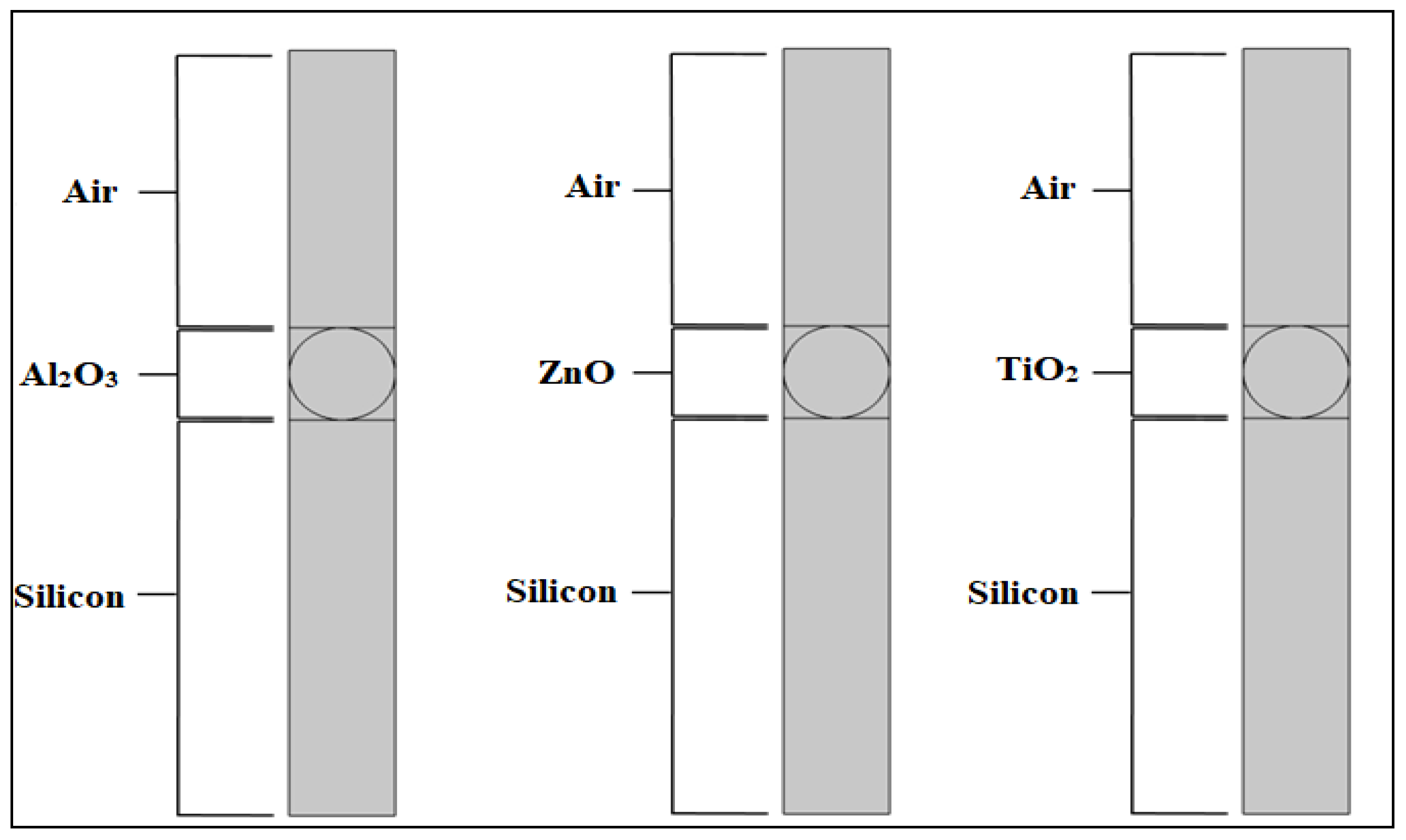
2.1. 2D Model Simulation and Analysis

Antireflection coatings using nanostructures can be divided into homogenous and non-homogenous layers according to the size distribution [32,33,34]. The homogenous layers have an advantage of reducing the light reflection more than the non-homogenous layers. This can be attributed to the controlled effective change of the refractive index from air to the Si surface. Several homogenous geometries have been reported, such as using cubic, spherical, and pyramidal nanostructures as an ARC layer [34].
To better build and simulate the problem model, and to reduce any artificial reflections, certain boundary conditions were selected. For this purpose, the four sides of the domain were chosen to be periodic boundaries when building the model using COMSOL Multiphysics. Equal spacing between the selected nanostructures was also imposed to produce the required domain periodicity. With this taken into consideration, the incident electromagnetic waves appeared with the same angular position on the opposite side of the structure. The top and bottom boundaries were set as identical to mimic a real-life device with their absorption, reflection, and transmission of the electromagnetic waves. On the other hand, and to reduce the demand for more computational power, the total incident energy was accounted for, and the S-parameter method was used to calculate the values of both reflectance and transmittance. The slit port boundary condition was used for the bottom layer to account for the electromagnetic wave source
The dimensions of the Si part of the 2D structure were typically taken as (8–104 nm) in width and 300 nm in length; immersed in air as (8–104 nm) in width and 200 nm in length, whereas the radius of the nanoparticles was considered as (5–50 nm) for the case of the spherical shape. Figure 1 shows the 2D schematic structure of the selected nanoparticles that were used in the design and simulation processes.

2.2. Operational Parameter Statistical Analysis

A statistical factorial analysis was conducted to study the effect of the nanoparticle type and size to be used as an ARC for Si solar cells (geometrical nanostructure: spherical shape) to produce the minimum reflection value along the visible light spectrum. Moreover, the geometrical parameters, including the structural dimensions, were varied for the selected shape and size in order to understand the light-matter interaction from this perspective, hence optimizing the surface reflectivity of the solar cell. Furthermore, the changes in the reflectance over the considered spectral range were taken into consideration for each nanoparticle size under study. The optimal parameters used for reducing reflections from the solar cell surface by an antireflective coating were analyzed by a standard RSM design called central composite design (CCD).

2.3. Continuous Factors

In order to obtain an optimized design which can be used to enhance the solar cell’s efficiency, and to reduce its reflectance, there are two continuous factors to be considered. One of them is the wavelength, which is considered to be in the range (380–720 nm), and the second one is the radius of the nanoparticle which is considered to be in the range (5–50 nm). The wavelength is usually the only factor studied in most studies, as it has great influence on the amount of light absorption [19,35]. Therefore, the influence of the wavelength range along the visible light spectrum is considered the most important parameter in solar cells’ performance. In this research, the COMSOL Multiphysics model considers wavelengths ranging from (380–720 nm), with a step size equal to 10 nm. The nanoparticles’ sizes were varied in the range of (5–50 nm) to investigate the size effect in the selected spectral range by using RSM.

2.4. Categorical Factors

Three different types of nanomaterials were considered as an antireflective coating (TiO2, Al2O3, and ZnO) due to their distinctive optical properties and because their refractive indexes match for Si. The average refractive indices in the desired spectral range of the considered materials (Si, Air, Al2O3, TiO2, and ZnO) are approximately 3.98, 1, 1.77, 2.61, and 2.02, respectively. Despite these values, and due to the change in the refractive index with the considered wavelength, the refractive indices were given as a set of data points as input to the model. Hence, the refractive index value designated for each considered wavelength value was accounted for. Factors affecting the final surface reflectance of the solar cell are not yet fully understood, and there is no way to connect these factors in direct relations. Explaining and clarifying these factors for optimization and implementation to increase the light absorption can highly reduce trial and error experiments and their associated costs.
Mathematical models describing the response were produced by using analysis of variance (full factorial), and experimental datasets were used to assess the fit of the models generated with the simulation data. For process optimization, 39 runs were used for a silicon solar cell with one replicate. Table 1 shows the process parameters and the considered ranges. Process parameters that were selected were nanoparticle radius, the wavelength spectrum, and nanomaterial type. In this RSM study, the considered levels were 4 nm, 11 nm, 28 nm, 45 nm, and 52 nm, in which both the 4 nm and 52 nm levels were outside the (5–50 nm) range in order to confirm the model validity at the boundaries.

3. Results and Discussion

3.1. Interpretation of Regression Model and Analysis

The analysis of variance (ANOVA) method was used to justify the suitability of the Si model. A reflectance model with a high F value and low p value indicates significant factors. The p value represents the probability of residual error involved in determining a certain factor as a significant factor. Normally, the effect of different factors must be below 0.05 in order to be considered as a significant factor, which represents a 95% confidence level. Table 2 displays the ANOVA for the second-order model proposed for reflectance given in the suggested model.
Based on the results in Table 2, in the reflectance model of Si (F value 12.33, p value 0.0002), all the main factors, A, B, AA, BB, AB, and AC, are significant with a p value less than 0.05%. The linear, square, and two-way interaction model equations were fitted for the reflectance response variable of silicon substrates. It is clear that the p value of the reflectance model for Si is less than 0.05, showing that the model is significant with a confidence level of ~95%. The reflectance model of Si shows that the R-square value is ~83.9%. For each factor, the model was developed to produce certain values representing the best-case scenario.
The statistical factors were estimated by using ANOVA. From the central composite design output, and the values shown in Table 2, a second-order polynomial regression model equation was derived to define the response in terms of the independent factors. The proposed mathematical model of silicon substrate reflectance is presented in the following equation:
R e f l e c t a n c e   ( S i ) = X [ 1.175 0.00238   ( R ) 0.00331   ( λ ) + 0.000365   ( R ) 2 + 0.000004   ( λ ) 2 0.000043   ( R λ ) ] + Y   [ 1.257 + 0.00287   ( R ) 0.00377   ( λ ) + 0.000365   ( R ) 2 + 0.000004   ( λ ) 2 0.000043   ( R λ ) ] + Z [ 1.163 0.00055   ( R ) 0.00343   ( λ ) + 0.000365   ( R ) 2 + 0.000004   ( λ ) 2 0.000043   ( R λ ) ]
where Y: predicted reflectance response, R: radius, λ: wavelength, (X, Y, Z): dummy factor (X: Al2O3, Y: TiO2, Z: ZnO). For example, if the material is TiO2, then Y = 1, (X and Z) = 0.

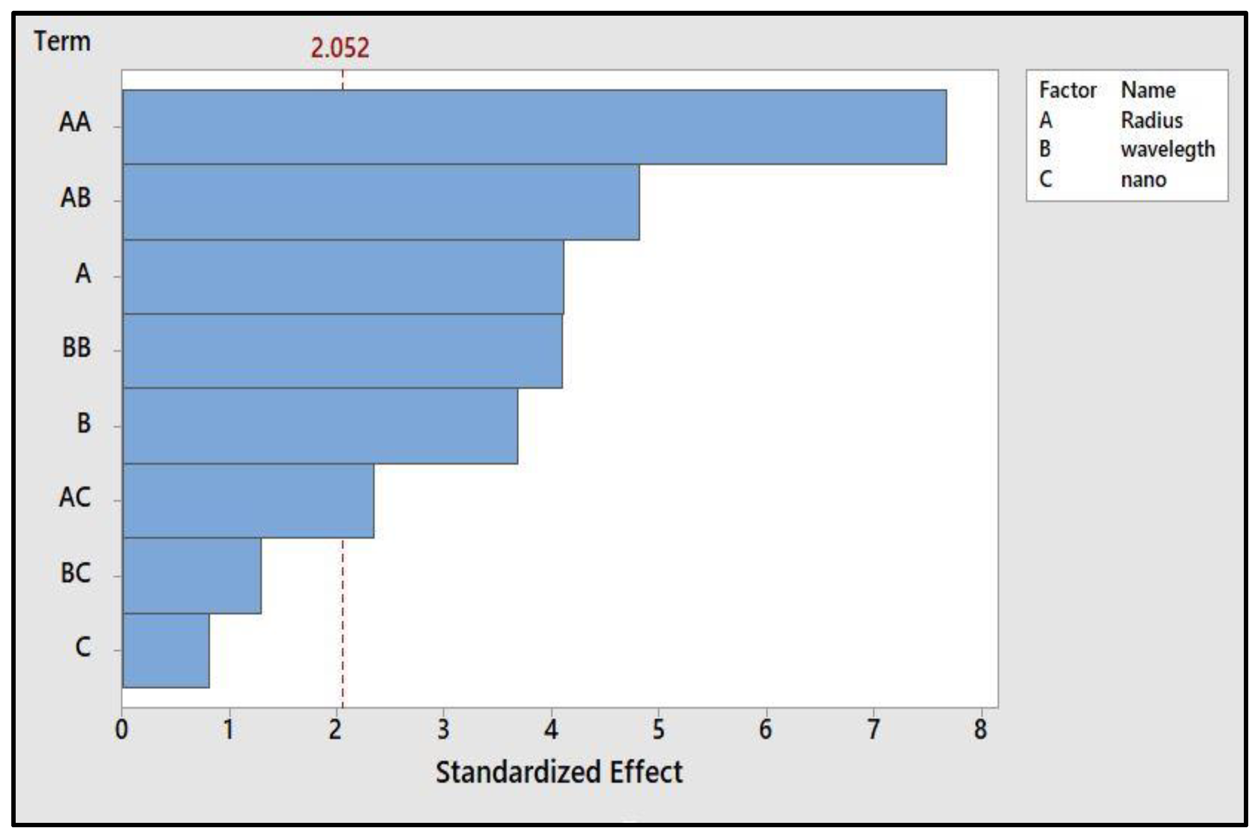
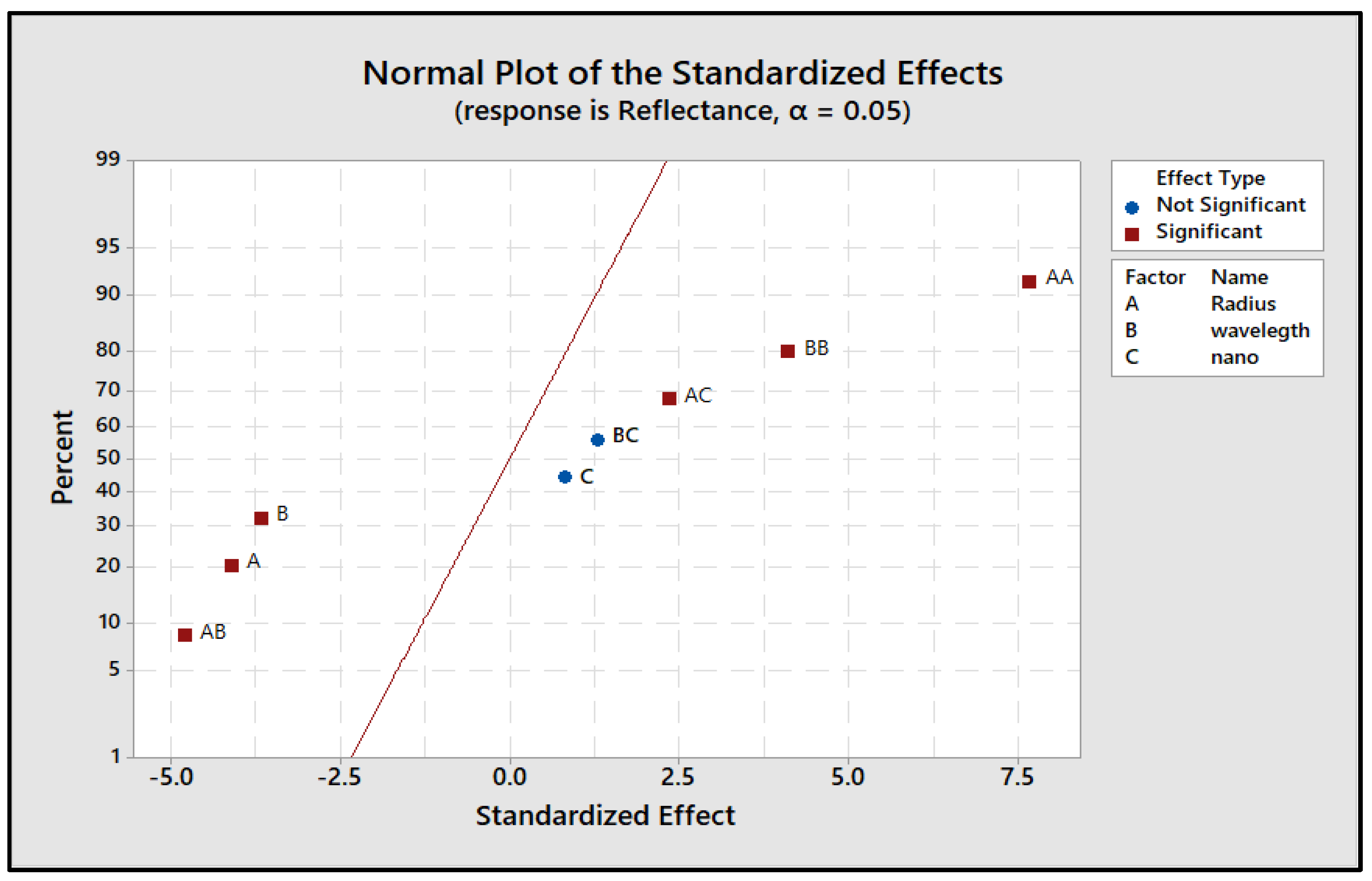
3.2. Estimation of Factor Effects

Analysis of the surface reflectance model of Si, and the effect of the independent factor data, began with the estimation of the effect of factors A, B, and C towards the response, which is the reflectance of the silicon surface, as shown in Table 2. From the ANOVA, it can be observed that factors A and B contribute the most significant effect toward output response, which is the reflectance. From the estimation effect analysis shown in Table 2, the normal plot for the standardized effects can be developed from the Pareto chart, as shown in Figure 2. The standardized effects show the significant factors towards the response “reflectance of silicon substrates”, which are A, B, AB, AC, BB, and AA. Each of them represents radius, wavelength, interaction between radius and wavelength, and interaction between the radius and nanomaterial type.
The guideline that was used for this analysis is based on a 95% confidence level. If there are any effects exceeding the 2.052 line, the effect is considered significant. Figure 2 shows factors AA, AB, A, BB, B, and AC that produce the most significant effects on the reflectance response. Based on the Pareto chart, factor A, which is nanoparticle size, has a direct effect on the reflectance. By changing the nanoparticle size, the reflectance value changes accordingly. The size of the nanoparticles changes the effective refractive index when it changes from air (n = 1) to Si (n~3.7) [36], as the nanoparticle coverage per unit area changes from smaller particles to larger particles [19,32,34]. However, according to the optical behavior of each material, different reflection values can be found from different materials at a certain considered nanoparticle size. On the other hand, factor B is found to have an effect on the reflectance response, which is the wavelength of the spectrum light. This factor is noted to be of great importance as different materials with different refractive indices have different reflectance values at each wavelength. These results are in agreement with published reports elsewhere [37,38]. Hence, the ARC behavior can be engineered in a selective manner to obtain a certain reflection level if needed for different applications, such as light reflectors, waveguides, or any other application that requires a certain level of reflectivity.
The Pareto chart displays the absolute value of factor effects. It can determine which factors have greater effects than others. The normal probability plot of the standardized effects was used to examine the magnitude and direction of factor effects on the surface reflectance of Si, as shown in Figure 3. Factors further from 0.0 on the x-axis have greater magnitude and are more statistically significant.
The direction of the main effects of all factors on the reflectance of the silicon cell was in agreement with the mathematical model equation described above. It is noted that the coefficients of (R)2 and (λ)2 both have positive values, which supports the location of AA and BB on the right side from 0.0, as shown in Figure 3. Similarly, the negative effects of AB, A, and B on the left side from 0.0 represents a decrease in the silicon cell reflectance, which can be achieved by increasing the values of R, λ, and as shown in the equation above. All the factors along the line can be ignored (BC and C). For the purpose of upgrading the model, factors AC, BC, and C can be removed from the full model analysis, because they are not significant. In order to optimize the surface reflectivity of the solar cell, the changes in the reflectance over the considered spectral range were taken into consideration for each nanoparticle size in the range of (5–50 nm) in this study. The standard RSM design, which is called central composite design (CCD), was used to find the optimal parameters of the antireflective coating for reducing reflections from the solar cell surface, as described in the contour plots below for the three nanoparticles used in this study.

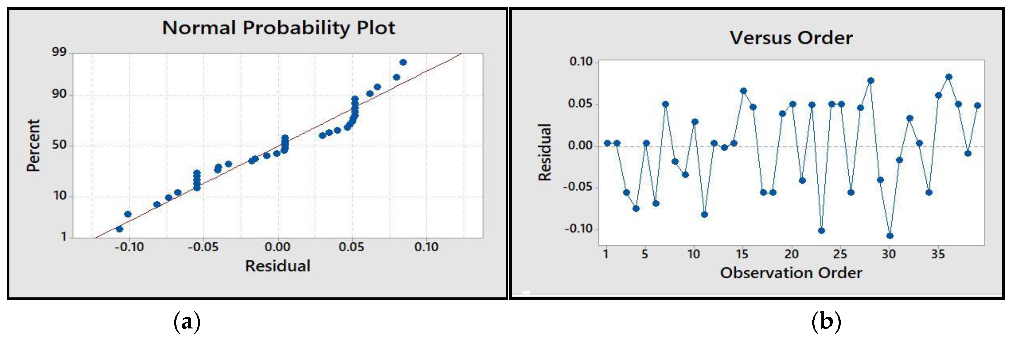
3.3. Interpretation of Residual Plots

In the ANOVA described above, it was assumed that all runs produced from the model were normally and independently distributed with the same variance at each level of the variables. These assumptions should be checked by examining the residuals and the residual plots produced from the ANOVA. A residual is the difference between each observation and its estimated (or fitted) value from the statistical model being studied [39]. These plots play an important role in assessing model adequacy and are used to examine the goodness-of-fit in regression. The normal probability plot of the residuals was used to verify the normality assumption. In this study, the normal probability plot of the residuals for the silicon cell followed a straight line, as shown in Figure 4a. If the residuals generally fall on a straight line, this indicates a good validity of the approximation of the linear regression model. In addition, a good variability between residuals and observation order is clear, as shown in Figure 4b. As the residuals fall in a horizontal band with no systematic pattern, no unusual structure is apparent, as shown in the versus order plot (Figure 4b). This means that the proposed model is adequate and there is no reason to presume any constant variance assumptions or violation of independence.

3.4. Response Surface Methodology—Interpretation of Contour Plots

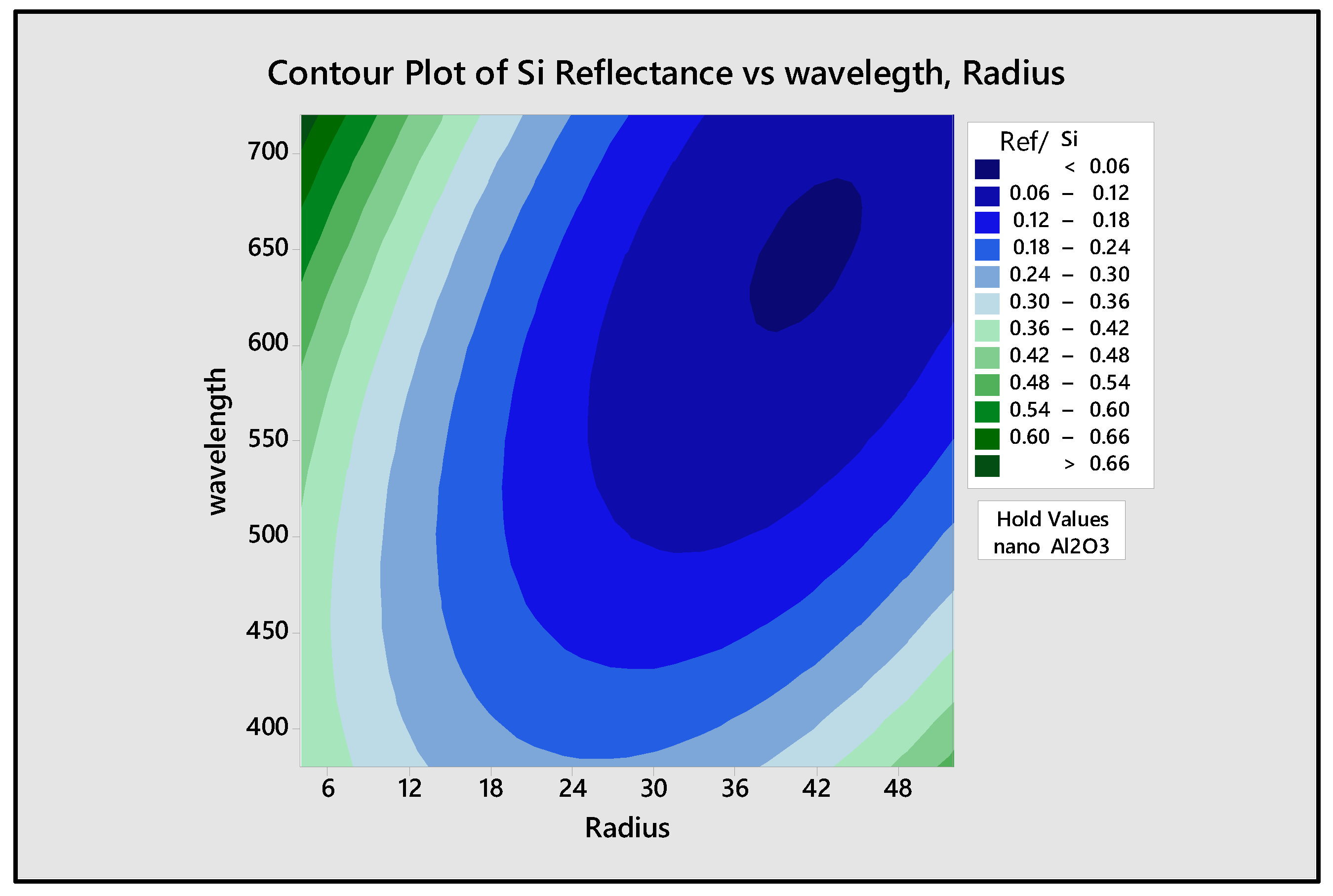
3.4.1. Aluminum Dioxide ARC Results

The 2D contour plot of the Al2O3 nanoparticle ARC depicts the interactive effects of two variables and their individual effect on the reflectance of Si, as shown in Figure 5. Here, the effects of the wavelength and the nanoparticle size of Al2O3 on the Si reflectance are presented. The minimum reflectance of Si (~5.57%) was achieved at a wavelength of ~644 nm, with an Al2O3 nanoparticle radius of ~41 nm, while the maximum silicon cell reflectance (>50%) was produced at wavelengths above 650 nm with an Al2O3 nanoparticle radius less than 12 nm. Other published reports show (~5%) reflection achieved by using both Al2O3 and TiO2 as double layer coatings [18,27] which, in general, can add more costs and complexity when used in an experimental setup. Therefore, the use of Al2O3 as a single layer ARC improves the overall process efficiency.

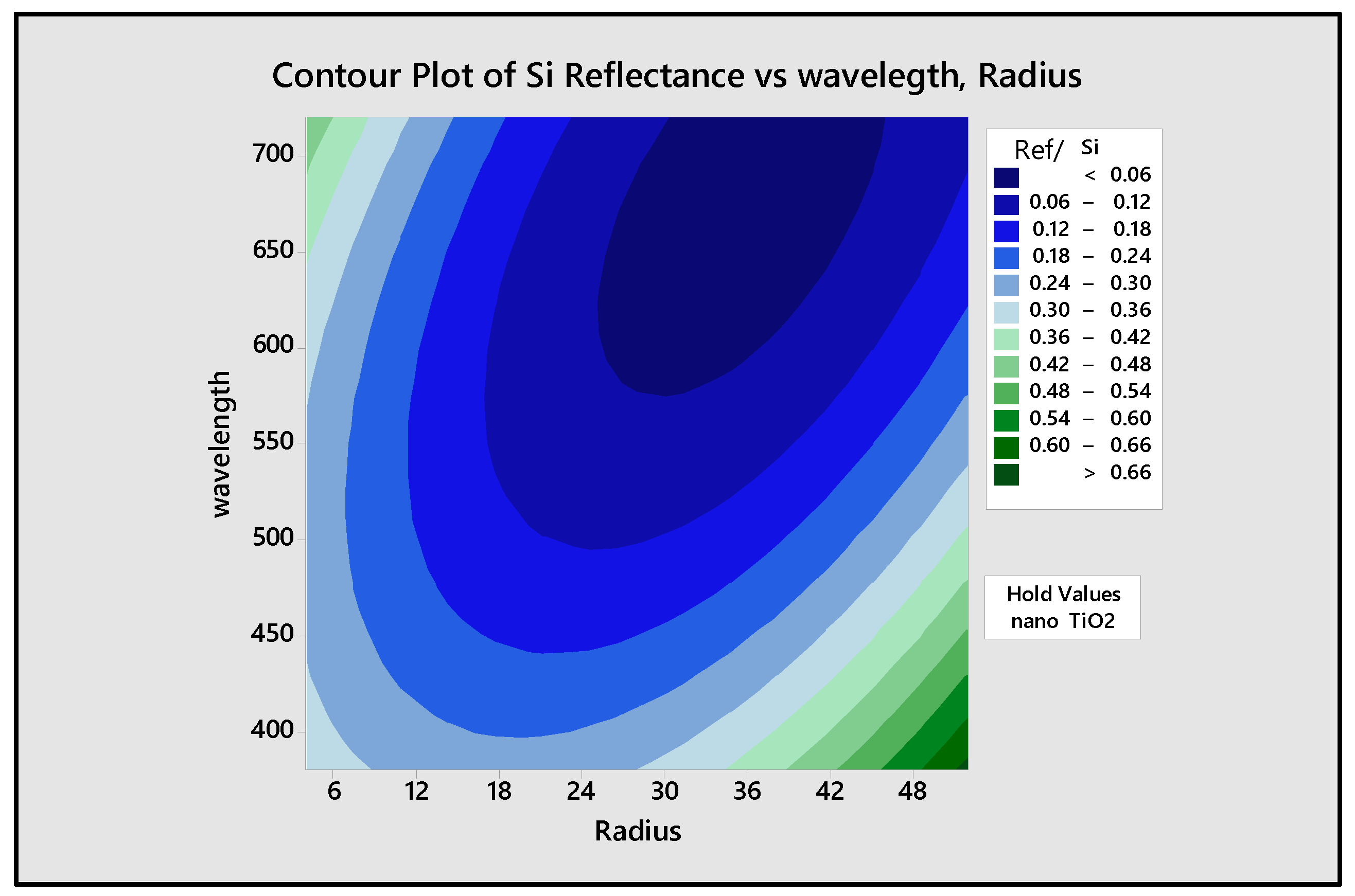
3.4.2. Titanium Dioxide ARC Results

Figure 6 shows the contour plot of TiO2 reflectance on Si with respect to nanoparticle size. From this figure, it can be seen that both wavelength and the TiO2 nanoparticle size have an influence on the surface reflectance of Si. As the radius increases from 5 to 36 nm, the surface reflectance of the silicon cell is decreased from the maximum, which is above (60%), to the minimum value (<6%). On the other side, in the region of wavelengths of less than 450 nm and with a radius more than 42 nm, the reflectance increases dramatically. Moreover, the minimum reflectance of Si with TiO2 nanoparticles (~3.24%) was achieved at the wavelength of 675 nm and nanoparticles with a radius of 36 nm, as shown in Figure 6. The achieved reflection value can highly enhance the solar cell’s efficiency when implemented in an experimental setup. Comparing the achieved value in this design with the (~5%) reflection by using double layers made of Al2O3 and TiO2 [18,27], or the (~7%) reflection by using a TiO2 single layer, gives the current results more significance for ARCs for Si [20,26,40].

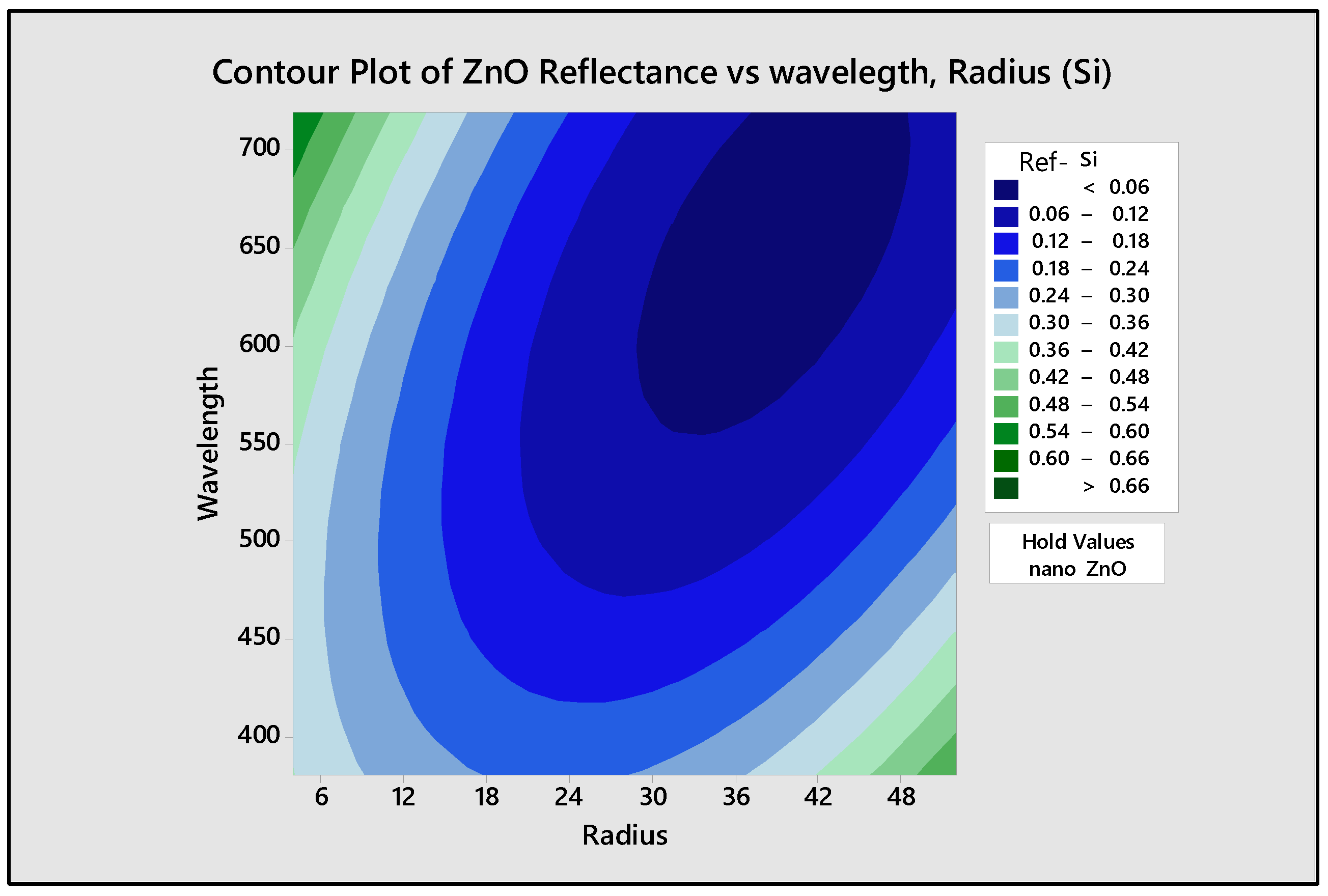
3.4.3. Zinc Oxide ARC Results

Figure 7 shows the contour plot of ZnO nanoparticles on Si, and the particle sizes with respect to the wavelength. Surface reflectance of Si was decreased in the region of wavelengths ranging from (550–720 nm) and a ZnO particle radius from (28-46 nm) to less than (6%), with minimum reflectance reaching (0%) with a ZnO nanoparticle radius of ~38 nm at a wavelength of 656 nm. Achieving near zero reflection for Si is of great importance, as it enhances the light absorption in the device structure dramatically. In this context, Jalali Alireza et al. Han Seung-Yeol et al. and others reported, on average, (3–4%) reflection values after using different sizes of ZnO nanoparticles as an ARC for Si, while in the current results it has been shown that near zero reflection can be achieved by using ZnO nanoparticles as an ARC layer for Si [16,41,42,43].

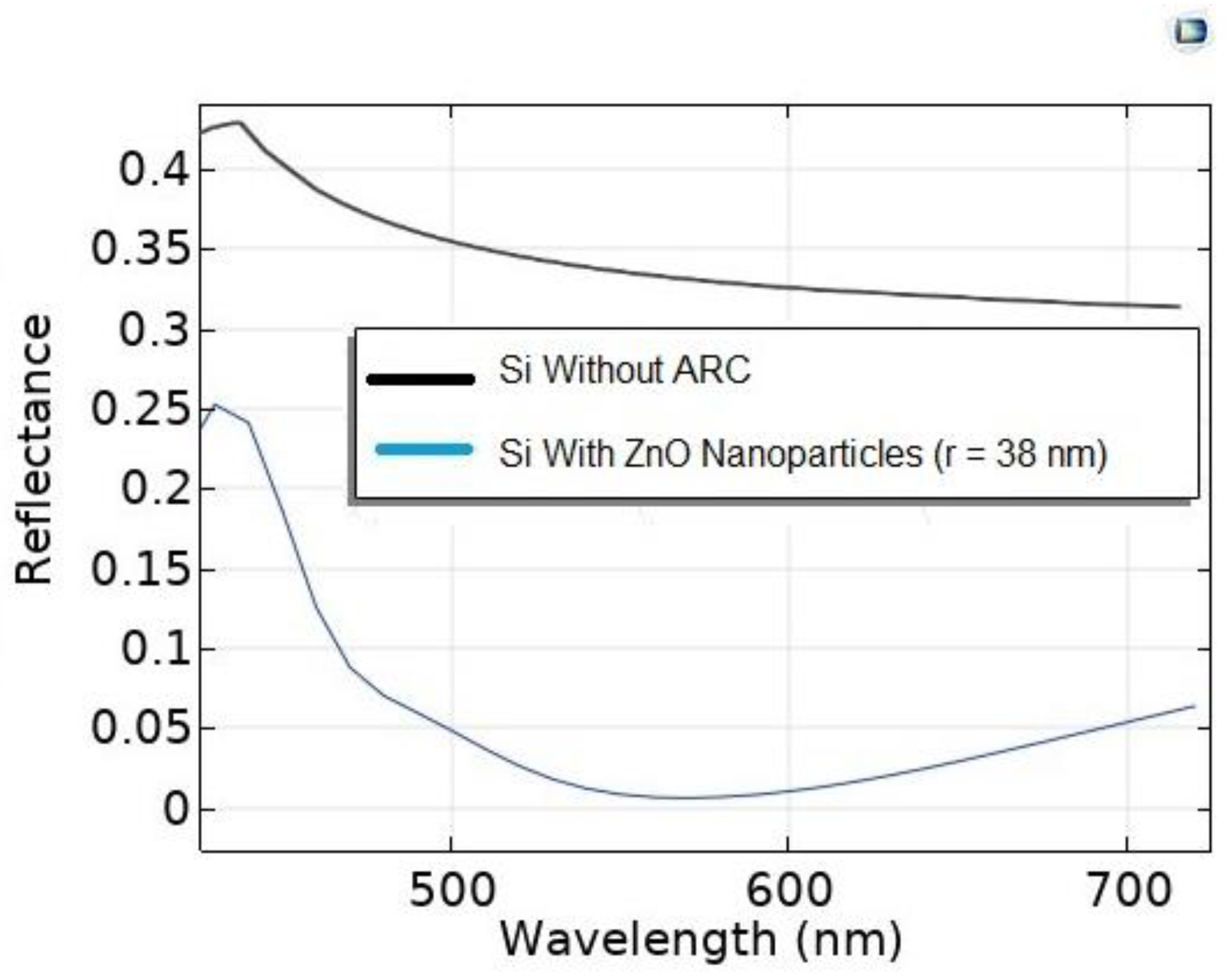
3.5. COMSOL Multiphysics Results

The spectral range study was done from (380–720 nm) for all three nanoparticle types, Al2O3, TiO2, and ZnO. The selected range is the range at which Si absorbs most of the light in the visible region to be converted into electrical power. The spherical structure shows different optical performances at different wavelengths. It is noted that the reflectance changes dramatically with the radius. The input parameters to the COMSOL model are shown in Table 3 below.
However, ZnO nanoparticles with a radius of ~38 nm showed a better reflection reduction when compared to the other studied types. The reflectance spectra of pristine Si and Si with ZnO nanoparticles are shown in Figure 8 below. The results reveal an average reflection percentage of (5%) along the selected spectral range, and approximately zero reflectance in the range (550–600 nm), which is in agreement with the RSM results. Table 4 shows summarized reflectance values for ZnO nanoparticles at different spectral ranges. With these results, it has been shown that Si can absorb most of the incident light found in the visible region when the Si has the highest external quantum efficiency. Hence, better power conversion efficiency can be obtained.

4. Conclusions

Silicon solar cells suffer from high reflection values due to their refractive index. Hence, reducing the reflection highly enhances the device performance. Antireflective coatings using nanomaterials can highly influence the reflection values, and bring down the surface reflection to near zero values to maximize the output power generated by Si solar cells. RSM-based optimization of the antireflection coatings by using the CCD method was used to evaluate and to optimize the effect of the nanoparticle types, radius of nanoparticles, and wavelengths to best reduce the reflection from the surface of Si. Three different types of nanoparticles, namely Al2O3, TiO2, and ZnO antireflective coatings on Si substrates, were modeled numerically by using finite element simulation by solving the Maxwell wave equation for periodic nanostructure arrays. COMSOL Multiphysics software was used to perform the simulation by selecting the electromagnetic wave optics module. Various factors, including radius of nanoparticles and wavelength period, were studied in order to obtain better insight into how the light-matter interaction is affected by changing the nanomaterial types.
Between the studied nanoparticle types, Al2O3 provides the worst optical performance. The TiO2 nanoparticles show intermediate optical performance, while the ZnO nanoparticles were the best to reduce the optical reflection by decreasing the light reflection to near zero. The optimization process shows less than 5% reflection values over a wide spectral range, while reaching near zero reflection at ~560 nm for a 38 nm ZnO nanoparticle size, which can highly enhance the solar cell performance.

Author Contributions

Conceptualization, Y.F.M., H.A. and G.T.; methodology, Y.F.M., H.A. and G.T.; software, Y.F.M. and H.A.; validation, Y.F.M. and H.A.; formal analysis, Y.F.M., H.A. and G.T.; investigation, Y.F.M., H.A. and G.T.; resources, Y.F.M. and G.T.; data curation, Y.F.M., H.A. and G.T.; writing—original draft preparation, Y.F.M., H.A. and G.T.; writing—review and editing, Y.F.M. and G.T.; visualization, Y.F.M. and G.T.; supervision, Y.F.M., H.A. and G.T.; project administration, Y.F.M. and G.T.; funding acquisition, Y.F.M. and G.T. All authors have read and agreed to the published version of the manuscript.

Funding

This research was funded by the Deanship of Scientific Research at Jordan University of Science and Technology—Jordan, grant number 20190533, in addition to the Jordanian Royal Hashemite Court under Innovative Projects in Nanotechnology.

Data Availability Statement

The data presented in this study are available on request from the corresponding author. The data are not publicly available due to ongoing study.

Conflicts of Interest

The authors declare no conflict of interest.

References

  1. Zheng, X.; Streimikiene, D.; Balezentis, T.; Mardani, A.; Cavallaro, F.; Liao, H. A review of greenhouse gas emission profiles, dynamics, and climate change mitigation efforts across the key climate change players. J. Clean. Prod. 2019, 234, 1113–1133. [Google Scholar] [CrossRef]
  2. Xing, Y.; Han, P.; Wang, S.; Liang, P.; Lou, S.; Zhang, Y.; Hu, S.; Zhu, H.; Zhao, C.; Mi, Y. A review of concentrator silicon solar cells. Renew. Sustain. Energy Rev. 2015, 51, 1697–1708. [Google Scholar] [CrossRef]
  3. Deshpande, R.A. Advances in Solar Cell Technology: An Overview. J. Sci. Res. 2021, 65, 72–75. [Google Scholar] [CrossRef]
  4. Jiang, T.; Xu, X.; Chen, G.Z. Silicon prepared by electro-reduction in molten salts as new energy materials. J. Energy Chem. 2020, 47, 46–61. [Google Scholar] [CrossRef]
  5. Lindroos, J.; Savin, H. Review of light-induced degradation in crystalline silicon solar cells. Sol. Energy Mater. Sol. Cells 2016, 147, 115–126. [Google Scholar] [CrossRef]
  6. Zarmai, M.T.; Ekere, P.N.N.; Oduoza, C.; Amalu, E.H. A review of interconnection technologies for improved crystalline silicon solar cell photovoltaic module assembly. Appl. Energy 2015, 154, 173–182. [Google Scholar] [CrossRef]
  7. Arduca, E.; Perego, M. Doping of silicon nanocrystals. Mater. Sci. Semicond. Process. 2017, 62, 156–170. [Google Scholar] [CrossRef]
  8. Zhang, H.; Wang, T.; Chen, W. Polyoxometalate modified all-weather solar cells for energy harvesting. Electrochim. Acta 2020, 330, 135215. [Google Scholar] [CrossRef]
  9. Diop, M.M.; Diaw, A.; Mbengue, N.; Ba, O.; Diagne, M.; Niasse, O.A.; Ba, B.; Sarr, J. Optimization and Modeling of Antireflective Layers for Silicon Solar Cells: In Search of Optimal Materials. Mater. Sci. Appl. 2018, 9, 705–722. [Google Scholar] [CrossRef]
  10. Singh, G. Solar power generation by PV (photovoltaic) technology: A review. Energy 2013, 53, 1–13. [Google Scholar] [CrossRef]
  11. Salman, K.A. Effect of surface texturing processes on the performance of crystalline silicon solar cell. Sol. Energy 2017, 147, 228–231. [Google Scholar] [CrossRef]
  12. Yin, Y.; Bu, Y.; Wang, X. PDMS-based subwavelength structures for broadband and wide-angle anti-reflection. Phys. B Condens. Matter 2020, 580, 411943. [Google Scholar] [CrossRef]
  13. Pillai, S.; Green, M. Plasmonics for photovoltaic applications. Sol. Energy Mater. Sol. Cells 2010, 94, 1481–1486. [Google Scholar] [CrossRef]
  14. Rehman, A.U.; Iqbal, M.Z.; Bhopal, M.F.; Khan, M.F.; Hussain, F.; Iqbal, J.; Khan, M.; Lee, S.H. Development and prospects of surface passivation schemes for high-efficiency c-Si solar cells. Sol. Energy 2018, 166, 90–97. [Google Scholar] [CrossRef]
  15. Shinen, M.H.; AlSaati, S.A.A.; Razooqi, F.Z. Preparation of high transmittance TiO2 thin films by sol-gel technique as antireflection coating. J. Phys. Conf. Ser. 2018, 1032, 012018. [Google Scholar] [CrossRef] [Green Version]
  16. Han, S.-Y.; Paul, B.K.; Chang, C.-H. Nanostructured ZnO as biomimetic anti-reflective coatings on textured silicon using a continuous solution process. J. Mater. Chem. 2012, 22, 22906–22912. [Google Scholar] [CrossRef]
  17. Oh, S.J.; Chhajed, S.; Poxson, D.J.; Cho, J.; Schubert, E.F.; Tark, S.J.; Kim, D.; Kim, J.K. Enhanced broadband and omni-directional performance of polycrystalline Si solar cells by using discrete multilayer antireflection coatings. Opt. Express 2012, 21, A157–A166. [Google Scholar] [CrossRef]
  18. Jung, J.; Jannat, A.; Akhtar, M.S.; Yang, O.-B. Sol–Gel Deposited Double Layer TiO2 and Al2O3 Anti-Reflection Coating for Silicon Solar Cell. J. Nanosci. Nanotechnol. 2018, 18, 1274–1278. [Google Scholar] [CrossRef] [PubMed]
  19. Makableh, Y.F.; Al-Fandi, M.; Khasawneh, M.; Tavares, C.J. Comprehensive design analysis of ZnO anti-reflection nanostructures for Si solar cells. Superlattices Microstruct. 2018, 124, 1–9. [Google Scholar] [CrossRef]
  20. Hocine, D.; Belkaid, M.; Pasquinelli, M.; Escoubas, L.; Simon, J.; Rivière, G.; Moussi, A. Improved efficiency of multicrystalline silicon solar cells by TiO2 antireflection coatings derived by APCVD process. Mater. Sci. Semicond. Process. 2013, 16, 113–117. [Google Scholar] [CrossRef]
  21. Lin, J.-Y.; Zheng, Q.; Hu, C.-S.; Lin, Y.-A. Reduction of silicon surface reflection with micro-sphere texturing. In Proceedings of the 2017 International Conference on Applied System Innovation (ICASI), Sapporo, Japan, 13–17 May 2017; Volume 2017, pp. 509–511. [Google Scholar] [CrossRef]
  22. Jo, H.-J.; Shim, B.-H. Efficiency enhancement of Cu(In,Ga)Se2 thin film solar cells by employing onmi-directional ZnO nanostructure with MgF2 anti-reflection-coating layer. Microw. Opt. Technol. Lett. 2018, 60, 2634–2639. [Google Scholar] [CrossRef]
  23. Ramelan, A.H.; Wahyuningsih, S.; Munawaroh, H.; Narayan, R. ZnO wide bandgap semiconductors preparation for optoelectronic devices. IOP Conf. Ser. Mater. Sci. Eng. 2017, 176, 012008. [Google Scholar] [CrossRef]
  24. Ahmad, A.A.; Al-Bataineh, Q.M.; Alsaad, A.M.; Samara, T.O.; Al-Izzy, K.A. Optical properties of hydrophobic ZnO nano-structure based on antireflective coatings of ZnO/TiO/SiO thin films. Phys. B Condens. Matter 2020, 593, 412263. [Google Scholar] [CrossRef]
  25. Bashirpour, M.; Forouzmehr, M.; Hosseininejad, S.E.; Kolahdouz, M.; Neshat, M. Improvement of Terahertz Photoconductive Antenna using Optical Antenna Array of ZnO Nanorods. Sci. Rep. 2019, 9, 1–8. [Google Scholar] [CrossRef] [PubMed]
  26. BashirKhanabc, S.; Zhangd, Z.; Lee, S.L. Single component: Bilayer TiO2 as a durable antireflective coating. J. Alloy. Compd. 2020, 834, 155137. [Google Scholar] [CrossRef]
  27. Юрпалoв, В.Л.; Федoрoва, Е.Д.; Дрoздoв, В.А.; Лавренoв, А.В. Оценка кислoтных свoйств систем B2O3–Al2O3и Pt/B2O3–Al2O3метoдoм зoндoвoй ЭПР-спектрoскoпии и их кoрреляция с прoтеканием сoвместнoй гидрoизoмеризации гептана и бензoла. Кинетика и Катализ 2016, 57, 548–553. [Google Scholar] [CrossRef]
  28. Chaya, B.M.; Sharon Prarthna, C.; Vinith Kumar, G.P.; Krishnaswamy, N. Modeling and Analysis of Double Layer Motheye Anti Reflective Coatings on Organic Light Emitting Diode. In Proceedings of the 7th International Conference on Photonics, Prague, Czech Republic, 25–27 February 2019; pp. 190–195. [Google Scholar]
  29. Refinery, N.P.; Braimah, M.N.; Odejobi, O.J. Utilization of Response Surface Methodology (RSM) in the Optimization of Crude Oil Refinery. J. Multidiscip. Eng. Sci. Technol. 2016, 3, 4361–4369. [Google Scholar]
  30. Paulo, F.; Santos, L. Design of experiments for microencapsulation applications: A review. Mater. Sci. Eng. C 2017, 77, 1327–1340. [Google Scholar] [CrossRef]
  31. Cao, B.; Adutwum, L.A.; Oliynyk, A.O.; Luber, E.J.; Olsen, B.C.; Mar, A.; Buriak, J.M. How to Optimize Materials and Devices via Design of Experiments and Machine Learning: Demonstration Using Organic Photovoltaics. ACS Nano 2018, 12, 7434–7444. [Google Scholar] [CrossRef] [Green Version]
  32. Wang, Y.; Hang, L. Study on transmission spectrum and electric field distribution of graded-index anti-reflection coatings. In Proceedings of the 9th International Symposium on Advanced Optical Manufacturing and Testing Technologies: Meta-Surface-Wave and Planar Optics, Chengdu, China, 26–29 June 2019; Volume 10841, p. 1084112. [Google Scholar]
  33. Sivakumar, R.; Gopalakrishnan, P.; Razak, M.S.A. Comparative analysis of anti-reflection coatings on solar PV cells through TiO2 and SiO2 nanoparticles. Pigment. Resin Technol. 2021. [CrossRef]
  34. Mousavi, B.K.; Mousavu, A.K.; Busani, T.; Zadeh, M.H.; Brueck, S.R.J. Nanostructured Anti-Reflection Coatings for Enhancing Transmission of Light. J. Appl. Math. Phys. 2019, 7, 3083–3100. [Google Scholar] [CrossRef] [Green Version]
  35. Al-Fandi, M.; Makableh, Y.F.; Khasawneh, M.; Rabady, R. Near zero reflection by nanostructured anti-reflection coating design for Si substrates. Superlattices Microstruct. 2018, 117, 115–120. [Google Scholar] [CrossRef]
  36. Kazanskiy, N.; Butt, M.; Khonina, S. Silicon photonic devices realized on refractive index engineered subwavelength grating waveguides-A review. Opt. Laser Technol. 2021, 138, 106863. [Google Scholar] [CrossRef]
  37. Elshorbagy, M.H.; Abdel-Hady, K.; Kamal, H.; Alda, J. Broadband anti-reflection coating using dielectric Si3N4 nanostructures. Application to amorphous-Si-H solar cells. Opt. Commun. 2017, 390, 130–136. [Google Scholar] [CrossRef]
  38. Rezaei, N.; Isabella, O.; Vroon, Z.; Zeman, M. Optical optimization of a multi-layer wideband anti-reflection coating using porous MgF2 for sub-micron-thick CIGS solar cells. Sol. Energy 2019, 177, 59–67. [Google Scholar] [CrossRef] [Green Version]
  39. Montgomery, D. C.; Runger, G.C. Applied Statistics and Probability for Engineers. Eur. J. Eng. Educ. 1994, 19, 383. [Google Scholar] [CrossRef]
  40. Visser, D.; Chen, D.Y.; Désières, Y.; Ravishankar, A.P.; Anand, S. Embossed Mie resonator arrays composed of compacted TiO2 nanoparticles for broadband anti-reflection in solar cells. Sci. Rep. 2020, 10, 1–11. [Google Scholar] [CrossRef] [PubMed]
  41. Minemoto, T.; Mizuta, T.; Takakura, H.; Hamakawa, Y. Antireflective coating fabricated by chemical deposition of ZnO for spherical Si solar cells. Sol. Energy Mater. Sol. Cells 2007, 91, 191–194. [Google Scholar] [CrossRef]
  42. Ilican, S.; Caglar, Y.; Caglar, M. Preparation and characterization of ZnO thin films deposited by sol-gel spin coating method. J. Optoelectron. Adv. Mater. 2008, 10, 2578–2583. [Google Scholar]
  43. Lee, Y.-J.; Ruby, D.S.; Peters, D.W.; McKenzie, B.B.; Hsu, J.W.P. ZnO Nanostructures as Efficient Antireflection Layers in Solar Cells. Nano Lett. 2008, 8, 1501–1505. [Google Scholar] [CrossRef] [PubMed]
Figure 1. A schematic diagram showing the Al2O3, TiO2, and ZnO nanoparticle 2D model placed on top of a Si substrate.
Coatings 11 00721 g001
Figure 2. Pareto chart of the standardized effects of Si.
Coatings 11 00721 g002
Figure 3. Normal plot of the standardized Si effects.
Coatings 11 00721 g003
Figure 4. (a) Normal probability plot for standardized residuals of Si, and (b) versus fits for standardized residuals of Si.
Coatings 11 00721 g004
Figure 5. Contour plot of Al2O3 reflectance vs. wavelength and radius.
Coatings 11 00721 g005
Figure 6. Contour plot of TiO2 reflectance vs. wavelength and radius.
Coatings 11 00721 g006
Figure 7. Contour plot of ZnO reflectance vs. wavelength and radius.
Coatings 11 00721 g007
Figure 8. Reflectance spectra of ZnO nanoparticles with radius 38 nm for Si cell obtained by COMSOL Multiphysics model.
Coatings 11 00721 g008
Table 1. The model process parameters and ranges.
SymbolProcess ParameterUnitRange
ARadius (R)nm5–50
BWavelength (λ)nm380–720
CNanomaterial type-Al2O3, ZnO, TiO2
Table 2. Analysis of variance of silicon solar cell (reflectance model).
SourceDFAdj SSAdj MSF-Valuep Value
Model110.5357810.04870712.330.0002
Linear
A, Radius (R)10.0667180.06671816.880.001
B, Wavelength (λ)10.0534800.05348013.530.003
C, Nanomaterial type20.0069380.0034690.880.427
Square
AA10.2324680.23246858.83>0.001
BB10.0664490.06644916.82>0.001
2-Way Interaction
AB10.0914240.09142423.140.011
AC20.0328660.0164334.160.027
BC20.0132480.0066241.680.206
DF: degrees of freedom, SS: sum of squares, F: F-test value, and p: error variance at a given response; parameters belonging to the filled cells are effective within 95% reliability interval.
Table 3. Input parameters to the COMSOL Multiphysics model.
Input ParametersDetails
GeometryNanoparticle size range: 5–50 nm
Nanoparticles Materials Al2O3, TiO2, and ZnO
Model PhysicsElectromagnetic wave frequency domain (emwf),
with the following boundary conditions:
- Top and bottom surfaces: Periodic
- Left and right sides: Floquet periodicity
Mesh sizePhysics-controlled mesh with element size (Fine)
Study● Type: Wavelength domain
● Unit: nm
● Range: 380–720 nm, with resolution: 10 nm
Table 4. Average reflectance values of using ZnO nanoparticles with radius 38 nm as an ARC layer.
Interval (nm)Reflectance
380–7205.5%
500–7202.3%
550–600~0%
Publisher’s Note: MDPI stays neutral with regard to jurisdictional claims in published maps and institutional affiliations.

