
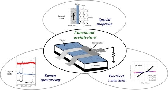
Iron Oxide-Coupled Graphite/Fe–Si Steel Structure for Analog Computing from Recycling Principle


Abstract
1. Introduction
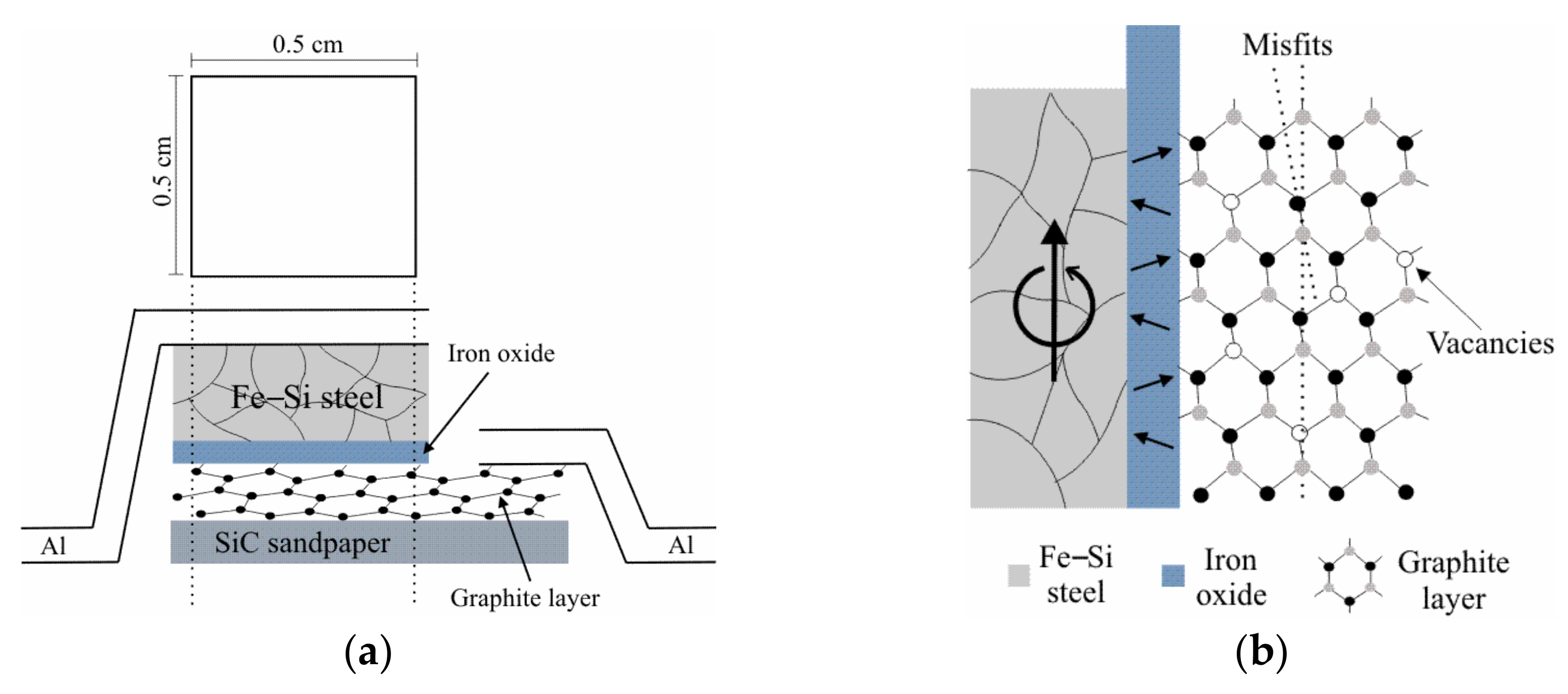
2. Materials and Processes
3. Results
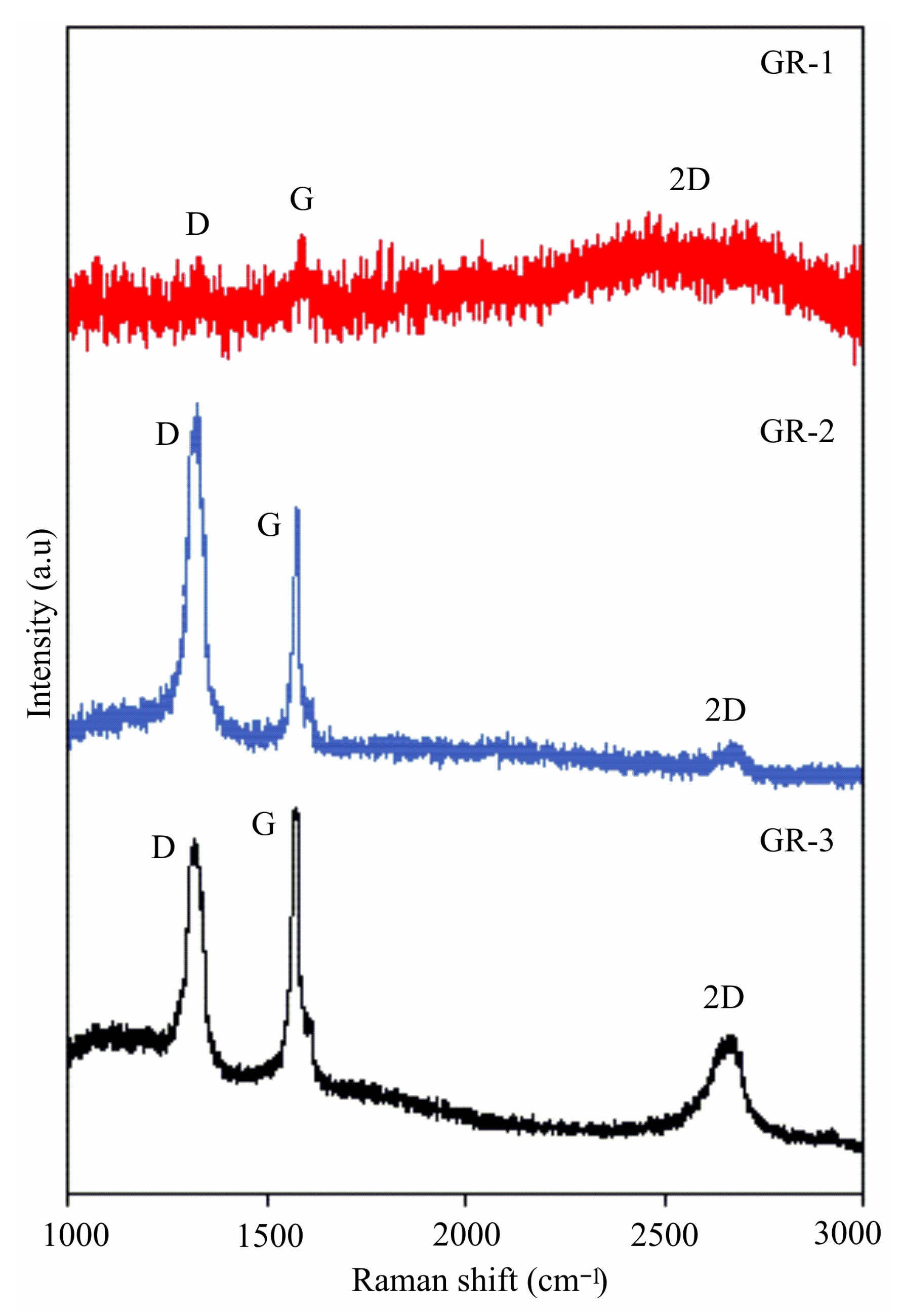
3.1. The Use of Raman Spectroscopy in the Analysis of Graphite Layers
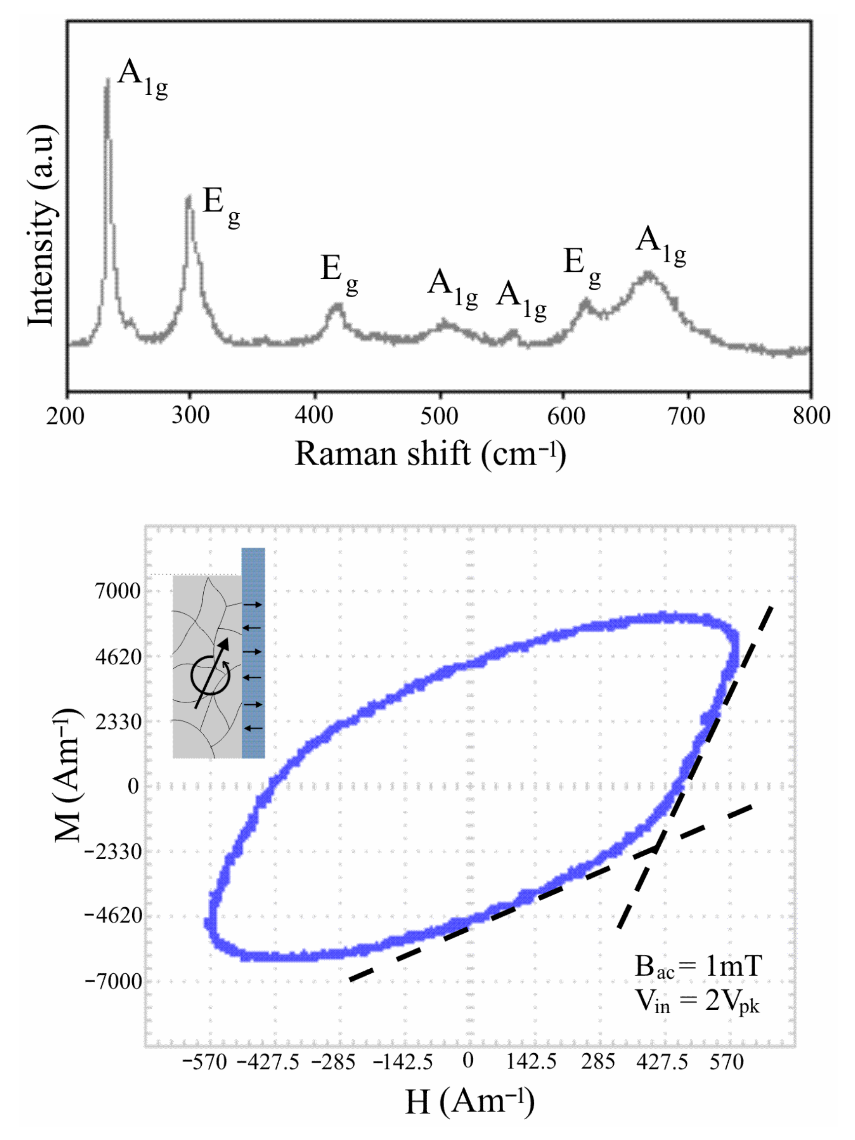
3.2. The Analysis of the Fe–Si Steel/Oxide Structure Using Raman Spectroscopy
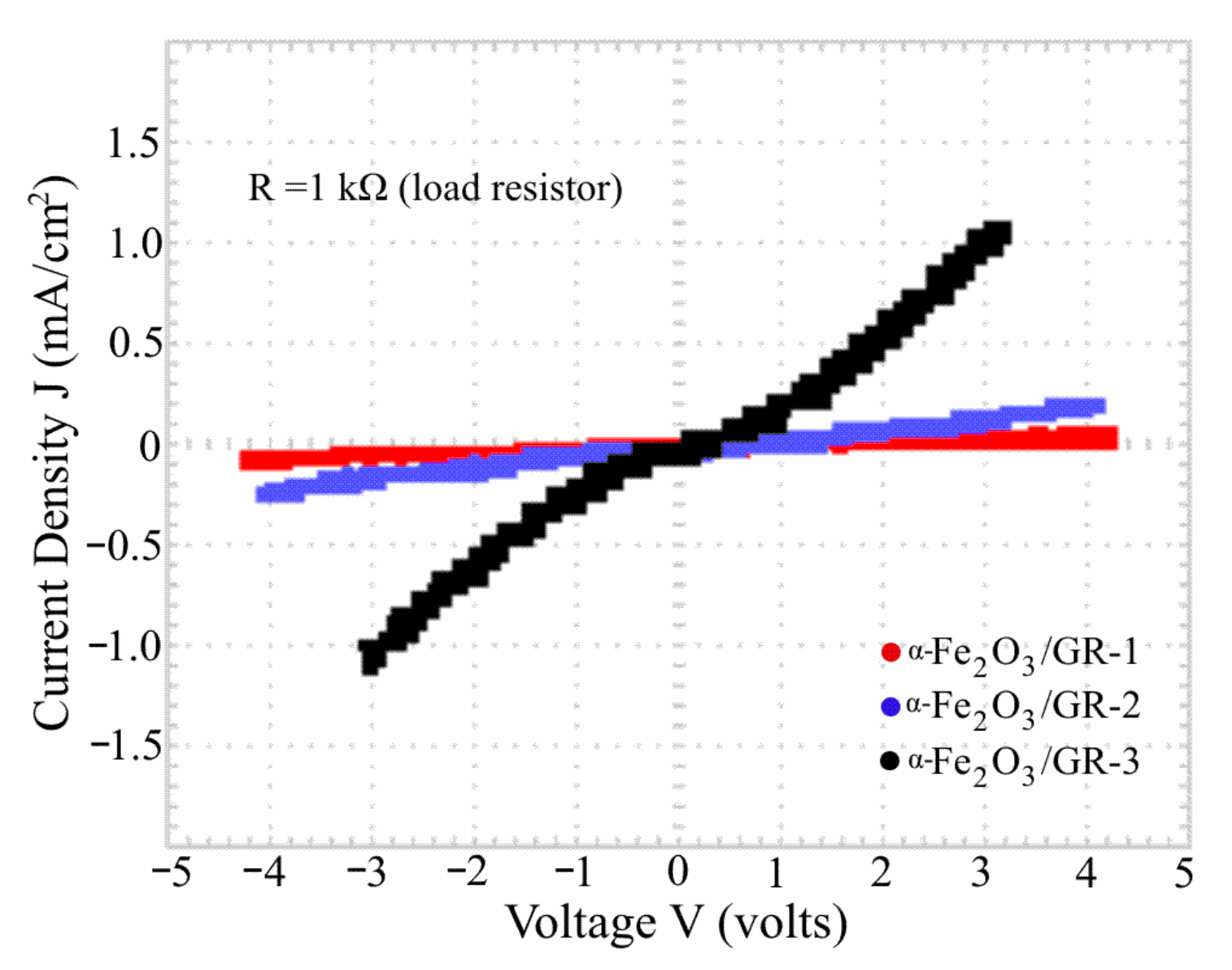
3.3. Current–Voltage Plots in the Current Injection Response of the Fe–Si Steel/α-Fe2O3/Graphite Structure
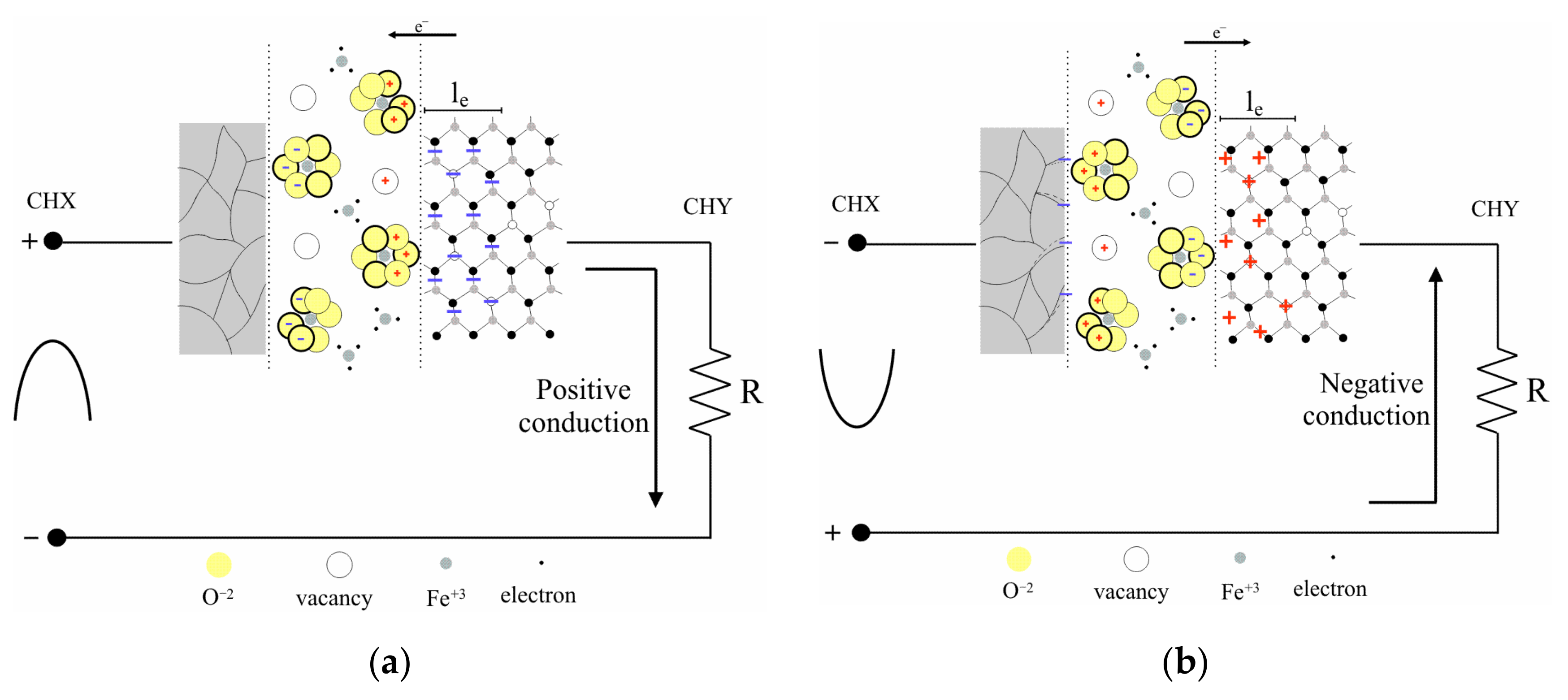
3.3.1. Conduction at Positive Half-Cycle
3.3.2. Conduction at Negative Half-Cycle
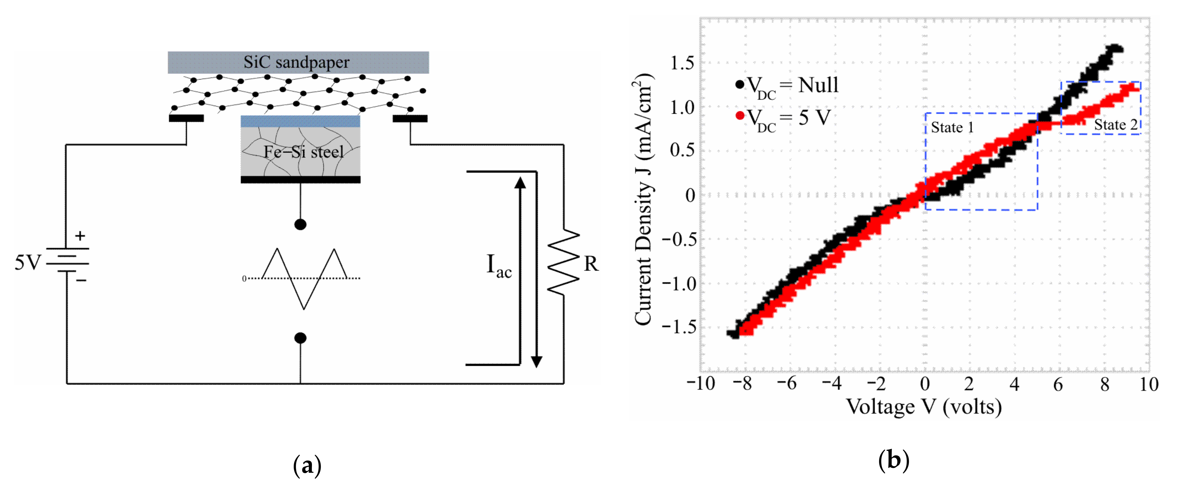
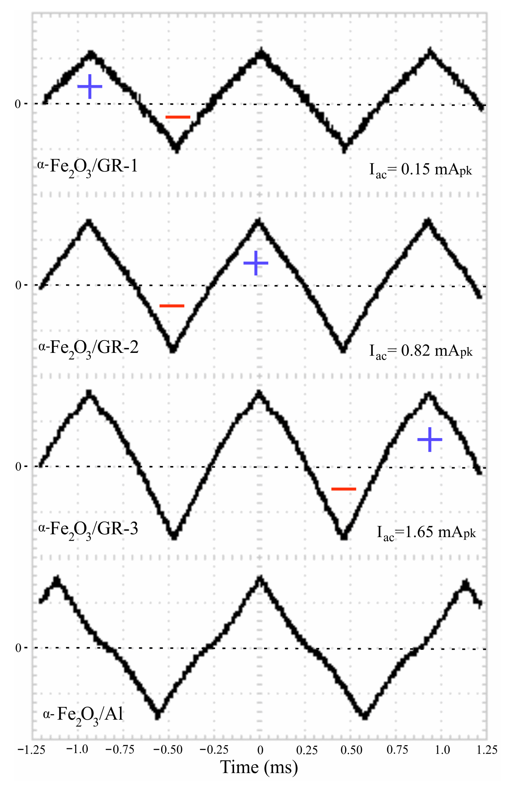
3.4. An Approach for Analog Computing Using the Fe–Si Steel/α-Fe2O3/Graphite Structure
4. Discussion
5. Conclusions
Funding
Institutional Review Board Statement
Informed Consent Statement
Data Availability Statement
Acknowledgments
Conflicts of Interest
References
- Blomsma, F.; Brennan, G. The emergence of circular economy: A new framing around prolonging resource productivity. J. Ind. Ecol. 2017, 21, 603–614. [Google Scholar] [CrossRef]
- Maina, S.; Kachrimanidou, V.; Koutinas, A. A roadmap towards a circular and sustainable bioeconomy through waste valorization. Curr. Opin. Green Sustain. Chem. 2017, 8, 18–23. [Google Scholar] [CrossRef]
- U.S. Geological Survey, Mineral Commodity Summaries 2020: U.S. Geological Survey. 2020. Available online: https://pubs.usg.gov/periodicals/mcs2020 (accessed on 1 April 2021).
- Norgren, A.; Carpenter, A.; Heath, G. Design for Recycling Principles Applicable to Selected Clean Energy Technologies: Crystalline-Silicon Photovoltaic Modules, Electric Vehicle Batteries, and Wind Turbine Blades. J. Sustain. Metall. 2020, 6, 761–774. [Google Scholar] [CrossRef]
- Baca, R. Recovery of electronics waste to be converting into functional devices. MRS Adv. 2019, 4, 1067–1075. [Google Scholar] [CrossRef]
- Fogarassy, C.; Finger, D. Theoretical and Practical Approaches of Circular Economy for Business Models and Technological Solutions. Resources 2020, 9, 76. [Google Scholar] [CrossRef]
- Ouyang, G.; Chen, X.; Liang, Y.; Macziewski, C.; Cui, J. Review of Fe-6.5 wt.% Si high silicon steel—A promising soft magnetic material for sub-kHz application. J. Magn. Magn. Mater. 2019, 481, 234–250. [Google Scholar] [CrossRef]
- Hunday, J.; Cernik, M.; Hilinski, E.; Predmersky, M.; Magurova, A. Influence of chemistry and hot rolling conditions on high permeability non-grain oriented silicon steel. J. Met. Mater. Miner. 2006, 304, e620–e623. [Google Scholar]
- Dresselhaus, M.S.; Dresselhaus, G. Intercalation compounds of graphite. Adv. Phys. 2002, 51, 1–186. [Google Scholar] [CrossRef]
- Cotton, A.; Wilkinson, G. Advanced Inorganic Chemistry, 4th ed.; John Wiley & Sons: New York, NY, USA, 2008. [Google Scholar]
- Baca Arroyo, R. Graphite Intended for Green Engineering Developed by Noncontaminant Reverse Abrasion. Adv. Mater. Sci. Eng. 2016, 2016, 7016457. [Google Scholar] [CrossRef]
- Manganaro, G. Advanced Data Converters, 1st ed.; Cambridge University Press: New York, NY, USA, 2012. [Google Scholar]
- Zarcone, R.V.; Engel, J.H.; Eryilmaz, S.B.; Wan, W.; Kim, S.; BrightSky, M.; Lam, C.; Lung, H.-L.; Olshausen, B.A.; Philip Wong, H.-S. Analog coding in emerging memory systems. Sci. Rep. 2020, 10, 6831. [Google Scholar] [CrossRef]
- Zhao, X.; Du, Y.; Liu, Y.; Du, Z.; Yuan, D.; Liu, L. Magnetostrictive properties of the grain-oriented silicon steel sheet under DC-biased and multisinusoidal magnetizations. Materials 2019, 12, 2156. [Google Scholar] [CrossRef] [PubMed]
- Mohamed, A.Y.; Park, W.G.; Cho, D.-Y. Chemical structure and magnetism of FeOx/Fe2O3 interface studied by X-ray absorption spectroscopy. Magnetochemistry 2020, 6, 33. [Google Scholar] [CrossRef]
- Cabrera, N.; Mott, N.F. Theory of the oxidation of metals. Rep. Prog. Phys. 1949, 12, 163–184. [Google Scholar] [CrossRef]
- Caplan, D.; Hussey, R.J.; Sproule, G.I.; Graham, M.J. The effect of FeO grain size and cavities on the oxidation of Fe. Corros. Sci. 1981, 21, 689–711. [Google Scholar] [CrossRef]
- Baca, R. Extraction of hysteresis parameters in foil magnetostrictive composites. Results Phys. 2019, 12, 2066–2068. [Google Scholar] [CrossRef]
- Theis, T.N.; Wong, H.-S.P. The end of Moore’s law: A new beginning for information technology. Comput. Sci. Eng. 2017, 19, 41–50. [Google Scholar] [CrossRef]
- Ferrari, A.C.; Meyer, J.C.; Scardaci, V.; Casiraghi, C.; Lazzeri, M.; Mauri, F.; Piscanec, S.; Jiang, D.; Novoselov, K.S.; Roth, S.; et al. Raman spectrum of graphene and graphene layers. Phys. Rev. Lett. 2006, 97, 187401. [Google Scholar] [CrossRef]
- Lübbe, M.; Gigler, A.M.; Stark, R.W.; Moritz, W. Identification of iron oxide phases in thin films grown on Al2O3 (0 0 0 1) by Raman spectroscopy and X-ray diffraction. Surf. Sci. 2010, 604, 679–685. [Google Scholar] [CrossRef]
- Shim, S.-H.; Duffy, T.S. Raman spectroscopy of Fe2O3 to 62 GPa. Am. Miner. 2001, 87, 318–326. [Google Scholar] [CrossRef]
- O’Dwyer, J.J. The Theory of Electrical Conduction and Breakdown in Solid Dielectrics, 1st ed.; Clarendon Press: Oxford, UK, 1973. [Google Scholar]
- Pendrys, L.A.; Zeller, C.; Vogel, F.L. Electrical transport properties of natural and synthetic graphite. J. Mat. Sci. 1980, 15, 2103–2112. [Google Scholar] [CrossRef]
- Sze, S.M.; Ng, K.K. Physics of Semiconductor Devices, 3rd ed.; Wiley: Hoboken, NJ, USA, 2007. [Google Scholar]
- Kim, M.-K.; Park, Y.; Kim, I.-J.; Lee, J.-S. Emerging materials for neuromorphic devices and systems. iScience 2020, 23, 101846. [Google Scholar] [CrossRef] [PubMed]
- Mizuchima, K.; Kinno, T.; Tanaka, K.; Yamauchi, T. Strong increase of the effective polarization of the tunnel current in Fe/AlOx/Fe junctions with decreasing Fe layer thickness. Phys. Rev. B 1998, 58, 4660. [Google Scholar] [CrossRef]
- Blundell, S. Magnetism in Condensed Matter, 2nd ed.; Oxford University Press: Oxford, UK, 2008. [Google Scholar]
- Liao, P.; Toroker, M.C.; Carter, E.A. Electron transport in pure and doped hematite. Nano Lett. 2011, 11, 1775–1781. [Google Scholar] [CrossRef] [PubMed]
- Bishop, M.D.; Hills, G.; Srimani, T.; Lau, C.; Murphy, D.; Fuller, S.; Humes, J.; Ratkovich, A.; Nelson, M.; Shulaker, M.M. Fabrication of carbon nanotube field-effect transistors in commercial silicon manufacturing facilities. Nat. Electron. 2020, 3, 492–501. [Google Scholar] [CrossRef]


| Sample | t (nm) | Rw (kΩ) | Rl (kΩ) | FWHM (cm−1) |
|---|---|---|---|---|
| GR-1 | 310 | 10.20 | 36.20 | 52.21 |
| GR-2 | 510 | 1.25 | 3.22 | 67.82 |
| GR-3 | 835 | 0.26 | 0.65 | 69.55 |
| M (Am−1) | Heff (Am−1) | FWHM (cm−1) | tan δ | RS (Ω) | LS (Hy) |
|---|---|---|---|---|---|
| 6891.16 | 569.89 | 103.32 | 1.12(δ = 48.25°) | 5.27 × 10³ | 7.5 × 10⁻³ |
| Interface | Ea (eV) | µaV (cm−1 V−1 s−1) | le (nm) |
|---|---|---|---|
| α-Fe2O3/GR-1 | 0.72 | 1.49 × 10¹⁷ | 25.42 |
| α-Fe2O3/GR-2 | 1.36 | 6.76 × 10¹¹ | 34.94 |
| α-Fe2O3/GR-3 | 1.84 | 6.63 × 10⁷ | 40.64 |
Publisher’s Note: MDPI stays neutral with regard to jurisdictional claims in published maps and institutional affiliations. |
© 2021 by the author. Licensee MDPI, Basel, Switzerland. This article is an open access article distributed under the terms and conditions of the Creative Commons Attribution (CC BY) license (https://creativecommons.org/licenses/by/4.0/).
Share and Cite
Baca-Arroyo, R. Iron Oxide-Coupled Graphite/Fe–Si Steel Structure for Analog Computing from Recycling Principle. Coatings 2021, 11, 607. https://doi.org/10.3390/coatings11050607
Baca-Arroyo R. Iron Oxide-Coupled Graphite/Fe–Si Steel Structure for Analog Computing from Recycling Principle. Coatings. 2021; 11(5):607. https://doi.org/10.3390/coatings11050607
Chicago/Turabian StyleBaca-Arroyo, Roberto. 2021. "Iron Oxide-Coupled Graphite/Fe–Si Steel Structure for Analog Computing from Recycling Principle" Coatings 11, no. 5: 607. https://doi.org/10.3390/coatings11050607
APA StyleBaca-Arroyo, R. (2021). Iron Oxide-Coupled Graphite/Fe–Si Steel Structure for Analog Computing from Recycling Principle. Coatings, 11(5), 607. https://doi.org/10.3390/coatings11050607