Abstract
Analog computing from recycling principle for next circular economy scenario has been studied with an iron oxide-coupled graphite/Fe–Si steel structure which was built using recycled waste materials, such as lead pencil and 3% Si steel (Fe–Si steel) foils. Proximity phenomena, such as disordered structure of iron oxide and magnetostriction-induced conduction, inside graphite lattice resulted in functional properties to advance analog architectures. Thermal oxidation was the synthesis route to produce iron oxide as coating film on Fe–Si steel foil, whose structure properties were validated by Raman spectroscopy where phase formation of hematite, α-Fe2O3, resulted as iron oxide thin-film. Three graphite layers with different compositions were also analyzed by Raman spectroscopy and used for studying electrical conduction in Fe–Si steel/α-Fe2O3/graphite structure from current–voltage plots at room temperature.
1. Introduction
Nowadays, sustainable polices and strategies are based on transition from a linear to a circular economy model, where worldwide research has presented an upward trend since 2015, matching with the aims of the 2030 Agenda [1]. Among the targets which must be addressed in the following years is advanced research on consequences of climate change; study efficient waste management to avoid a negative environmental impact; growth of agricultural activities; innovation in sustainable processes, goods, and services; and recycling of waste materials [2,3]. In this way, waste will become a valuable resource that must be reintroduced into the manufacturing processes; therefore, seeking material attributes (stable chemical properties, electrical, magnetic, and mechanical robustness, etc.) is still ongoing.
The attention for recycling principle has grown considerably, both for fundamental research and for novel applications [4]. Recycling principle is focused on preventing either burning to recover some of the metals or else grinding wastes up and treating, and instead recovering 90% or more of valuable materials (gold (Au), silver (Ag), copper (Cu), iron (Fe), silicon (Si), graphite and others) through the zero-wastewater and zero-carbon dioxide emissions; avoiding these results in stationary storage for long periods of time, which might result in a black mass with dangerous solvents and tens of thousands of tons of waste entering into the landfills. Therefore, as electrical and electronic hardware production soars, so does interest in recycling, these being one of the largest sources of waste of clearly a lot of value. Rather than dismantling a hardware pack into cells and discharging them, they can be separated in modules and studied separately to identify their special properties [5]. Due to the abundance and industrial usage today for development of worldwide items, recycling 3% Si steel and graphite as building blocks of emergent devices could be better than if these are, rather, long-lasting waste sources [6].
Fe–Si steels play an important role in energy systems, where these are mainly used for manufacturing core-laminated transformers and rotating engines. Three percent Si steel-laminates have been widely used in electrical built-in home appliances, such as portable radios, ventilation systems, pump systems, lighting sources, and others, where low core losses and high permeability are required for the Fe–Si steels [7]. For commercial 3% Si steel grade, well-referred here as Fe–Si steel, their chemical composition must be intentionally modified to improve magnetic properties by adding 0.4% silicon, 0.33% aluminum, 0.55% manganese and 0.013% phosphor in percent per weight in accordance to previous studies [8]. These magnetic properties are strongly influenced by microstructural parameters such as grain size, residual stresses and crystallographic texture.
Graphite is one of the available intercalated compound-based materials with a weak interlayer interaction between individual graphene sheets, consisting of the mixture of clay particles, mainly silicon dioxide (SiO2) and a minor amount of metal oxides in graphite lattice [9,10]. During the accommodation of clay particles it is expected that carbon atom vacancies and lattice defects in-plane and out-plane of the graphite structure occur, which make graphite a good lubricant and a lead pencil that people use in their daily life for writing, sketching, etc. For a long time, graphite, as an isolated layer, has been well studied, but its physical properties for engineering application became available in 2016 [11]. One direction that today shows promising result is assembling graphene layers (stacked graphite) on silicon carbide (SiC) substrate by reverse abrasion technique, where the control over the coverage percentage and thickness are advantageous; here, low carrier mobility about 250 cm2/Vs (several order of magnitude lower than in silicon), scattering mean free path l = 235 nm, and middle conductance at room temperature might allow charge carriers to move independent of their energy and space-charge-limited conduction (SCLC) inside the graphite bulk at nearly the length from their interface.
Today, analog computing is proposed and studied extensively to be capable of executing easily arithmetic functions at much lower power consumption than digital solutions. An analog scheme can allow versatile conduction modes under a wide range of conditions, which means that continuous time processing will be more beneficial than discrete time processing [12,13]. Thus, seeking ecofriendly alternatives for analog computing within a reduced number of building blocks is of importance. So, too is motivating research systems out of equilibrium, such as iron oxide-coupled Fe–Si steel, which might induce magnetostrictive behavior by perpendicular current injection inside the graphite layers. In this case, proximity effects by coexisting magnetostriction and disorder in lattice structure at the iron oxide surface might be responsible for functional properties in the Fe–Si steel/oxide interface when alternating current signal is injecting in a Fe–Si steel/iron oxide/graphite structure [14,15]. Thereby, the work presents the salient experimental observations of an iron oxide-coupled graphite/Fe–Si steel structure to understand how exchange interactions at the interface of iron oxide/Fe–Si steel can induce SCLC in graphite layers of different compositions. Stages of synthesis and parameters to build and analyze the structure will be explained in Section 2. Results on structure formation in graphite and iron oxide, phenomenological description of the current injection response and an example for analog computing in a practical structure will be covered in Section 3. Section 4 describes the discussion of the previous studies and hopeful findings with the theoretic analog device architecture useful as an arithmetic processor. Finally, conclusions about this research are presented in Section 5.
2. Materials and Processes
To study physical properties in the iron oxide-coupled graphite/Fe–Si steel structure, a methodology was developed based on probing dynamic action at two interfaces in the schematic of Figure 1. The proposed structure included one graphite layer physically assembled on silicon carbide (SiC) sandpaper as a flexible substrate and one iron oxide thin-film grown on the Fe–Si steel foil by thermal oxidation. Both layers were mechanically joined between two large-area aluminum electrodes (1 cm wide × 3 cm in length), as shown in Figure 1a, to achieve a proximity coupling into the active region of area (0.5 cm × 0.5 cm), where the iron oxide thin-film must act as a quasi-insulating layer to drive the conducting channel of the charge carrier´s in the space-charge-limited conduction (SCLC) regime. Figure 1b shows the assembling diagram of all the layers involved in the whole structure engineered here, where magnetic character in Fe–Si steel and iron oxide layers was initially defined by equilibrium states (random arrows showing magnetic moments), and disorder in the graphite matrix depended on misfits and vacancies occurring as a function the mechanical accommodation on the SiC surface. Two interfaces emerged from the structure: first, Fe–Si steel/iron oxide; second, iron oxide/graphite layer.
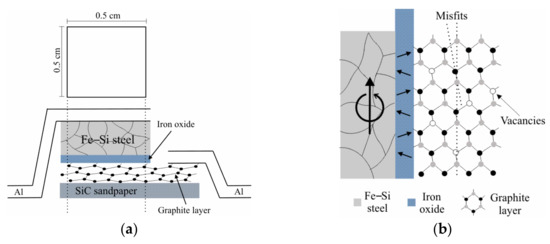
Figure 1.
Iron oxide-coupled graphite/Fe–Si steel structure: (a) Schematic diagram of the physical array fabricated; (b) assembly of the three regions where is shown their magnetic and structural character.
In the fabrication of the structure processed here, the following two stages were involved: (1) Lead pencil rods were used as graphite source to grow the graphite layers of three different thicknesses assembled on SiC sandpaper using the reverse abrasion technique [11], where the sizes of these layers were 0.5 cm wide and 2 cm in length. (2) Fe–Si steel foil with 3% Si steel grade, of an average thickness of 0.18 mm, recovered from a useless low power core-laminated transformer, was used as substrate for synthesis of the iron oxide thin-film.
It is well known that effects such as influence of temperature, humidity of the atmosphere, oxidation time and controlled diffusion along grain boundaries at low temperatures (<500 °C) are expected to play a major role in the oxidation kinetic [16,17]; therefore, in order to achieve better adherence of the oxide on the Fe–Si steel foil, and more uniformity of its thickness in nanometer scale, to be useful as the coating layer responsible for the structure performance of Figure 1, the following stages were accomplishing for their preparation: (a) Fe–Si steel foil was cut to a cross-section area of 1 cm × 2 cm and both upper and bottom sides of the foil were mechanically grounded using 1200 grit SiC paper; (b) the Fe–Si foil was cleaned with home-used organic solvent, known as thinner, and dried for about 2 h in ambient atmosphere; (c) a sealed laboratory furnace to avoid gas leakage was used; (d) air (21% O2, 79% N2) was chosen as oxidizing atmosphere; (e) after 30 min, the furnace temperature was stabilized, then Fe–Si steel foil was introduced into the quartz tube; (f) thermal oxidation was performed at 250 °C for a duration of 60 min. Finally, next to the oxidation stage, the sample was cooled out of the quartz tube, whose average thickness of the dark blue iron oxide was ~120 nm and was estimated by a profilometer (KLA Tencor, P15, Milpitas, CA, USA).
Structure formation of graphite layers and iron oxide grown on Fe–Si steel foil was investigated by Raman spectroscopy to know their associated bands; the Micro-Raman System (HORIBA Jobin-Yvon, HR800, Piscataway, NJ, USA) of excitation line λ = 632.8 nm (He-Ne laser) at 20 mW and 50× objective was used to avoid laser-induced heating.
Current signal injection response was performed and evaluated by current–voltage plots at room temperature using a digital storage oscilloscope (Tektronix, TDS1012C, Beaverton, OR, USA). In addition, a correlation study between low-field magnetic ordering and structure formation was addressed, using a methodology before reported, to evaluate hysteresis parameters such as magnetization, M, effective field strength, Heff, loss coefficient, tan δ, equivalent resistance, RS, and equivalent self-inductance, LS, in magnetostrictive composites based on a series resistor-inductor-capacitor (RLC) circuit [18].
3. Results
This section describes how defects in graphite layers and magnetostriction in the Fe–Si steel/oxide interface may be clearly activated at their surface, and how their spatial distribution may define the conducting channel with the change in the current signal injection. It then reviews Raman bands and electrical conduction to understand their origin in iron oxide-coupled graphite/Fe–Si steel structure, with emphasis on the evaluation of their physical parameters, and phenomenological description during current signal injection is correlated with exchange phenomena. An example for analog computing is confirmed to elucidate how a simpler arithmetic processor would optimize signal processing in electronics [19].
3.1. The Use of Raman Spectroscopy in the Analysis of Graphite Layers
Samples of graphite layers reveal three characteristic peaks, as shown in Figure 2. In sample GR-1, these peaks are located at 1333.25 cm−1 (D band), 1586.79 cm−1 (G band) and 2432.10 cm−1 (2D band), while sample GR-2 exhibits peaks sited at 1333.41 cm−1 (D band), 1557.46 cm−1 (G band) and 2689.22 cm−1 (2D band), and for the sample GR-3, the peaks are found at 1331.77 cm−1 (D band), 1557.92 cm−1 (G band), and 2681.52 cm−1 (2D band), respectively.
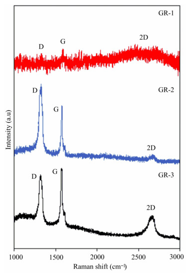
Figure 2.
Raman spectra of three different graphite layers, where behavior of each assigned band indicates how composition of graphite was made.
Raman spectra demonstrate that graphite layers have a relatively simple structure; however, slight peak displacements are observed, which means that each layer differs only in the relative position of their carbon atoms stacked together and the nature of their disordered bonding to one another. It is well known that the D band represents a ring separating mode from sp2 carbon atoms, which defines defects formation in the graphite matrix. The G band is an in-plane vibrational mode involving the sp2 hybridized carbon atoms, which are very depended to the number of stacked layers present in each sample. Finally, the 2D band is the result of two phonon-lattice vibrational process at the c axis inside the graphite matrix; however, is independent and thus is not activated by proximity to a defect [20].
Table 1 summarizes the assessed parameters from the graphite samples, such as the thickness, t, distributed wide resistance, Rw, distributed length resistance, Rl, and full width at half maximum (FWHM) of defects D band for each sample tested under this study. The thickness of the samples was determined by a profilometer, KLA Tencor, which resulted in accordance to the intensity of the G band, giving insights for the growing number of layers.

Table 1.
Physical parameters for the synthesized graphite layers.
3.2. The Analysis of the Fe–Si Steel/Oxide Structure Using Raman Spectroscopy
Raman spectra of Figure 3 show peaks located at 233.67 cm−1 (A1g), 300.31 cm−1 (Eg), 420.21 cm−1 (Eg), 511.41 cm−1 (A1g), 562.42 cm−1 (A1g), 621.11 cm−1 (Eu) and 672.76 cm−1 (Eu), respectively. The widest of the bands assigned from 200 to 520 cm−1 match with the corundum-type defective structure related to hematite (α-Fe2O3), because the Fe-O exchange interactions depended on the presence of the oxygen vacancies in α-Fe2O3 [21]. However, the band from 550 to 800 cm−1 obeys with magnetostrictive defects induced by discontinuous grain growth and the slight displacement of domain walls as a function of their added chemical composition (silicon, aluminum, manganese, and phosphor) in the 3% Si steels [22]. A correlation study to understand the importance of the α-Fe2O3 phase and the widest band from 550 to 800 cm−1 was done here using a series RLC circuit to calculate hysteresis parameters, likewise as in [18], which was comprised of a cylindrical inductor of length 1.5 cm that comprises 180 turns of 28 size from American Wire Gauge (AWG) standard, inner diameter of 2.5 cm, outer diameter of 3.2 cm, a capacitor of 2.2 nF and resistor of 100 Ω.
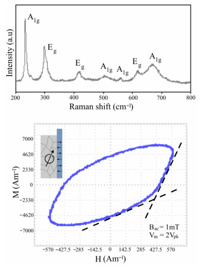
Figure 3.
Correlation study in the Fe–Si steel/iron oxide structure, whereby the Raman spectra of the iron oxide thin-film reveals hematite phase and M-H loop for the iron oxide-coupled Fe–Si steel foil exhibited exchange coupling.
Extracted correlation parameters in the Fe–Si steel/α-Fe2O3 interface are registered in Table 2, where the magnetization-field strength loop, referred here as the M-H loop, in Figure 3 was extracted and displayed on the oscilloscope screen, by using the XY mode function incorporated in the digital storage oscilloscope, under specific test conditions (inset in Figure 3), such as externally applied magnetic field, Bac, and excitation sine wave, Vin, for the series RLC circuit. The asymmetric magnetic ordering was confirmed at room temperature in the Fe–Si steel/α-Fe2O3 interface, where strong short-range Fe–O–Mn interactions inside the Fe–Si steel lattice are in accordance with larger equivalent resistance RS, revealing that surface conduction in α-Fe2O3 might certainly influence exchange coupling above a critical current amplitude. This is associated with internal magnetization, M, and effective field strength, Heff, but also larger equivalent self-inductance, LS, as shown by the slope shift of the two dashed arrows in Figure 3. This might allow for a nonlinear growing current conduction inside the somewhat arithmetic processor, akin to that in Figure 1, away from the α-Fe2O3/graphite interface at partially occupied defect sites by the presence of randomly trapped charge.
Table 2.
Correlation parameters evaluated in the α-Fe2O3/Fe–Si steel structure.
3.3. Current–Voltage Plots in the Current Injection Response of the Fe–Si Steel/α-Fe2O3/Graphite Structure
Performance of the Fe–Si steel/α-Fe2O3/graphite structure was confirmed, with the measuring strategy of Figure 4a,b, to understand how electrical conduction occurs at the α-Fe2O3/graphite interface, using three graphite layers, labeled as GR-1, GR-2 and GR-3, analyzed in Figure 2. A sine wave was generated by a function generator (Matrix, MFG-8250A). The frequency of the sine wave was 1 kHz with bipolar voltage magnitude of ±10 Vpk (peak voltage). A load resistor R = 1 kΩ was chosen to measure the output voltage and thus calculate the current magnitude by Ohm’s law. The sine wave was connected in series with aluminum electrodes, similar to Figure 1a. To evaluate the electrical response of the α-Fe2O3/graphite interface when an alternating conduction was carried, current–voltage plots were experimentally extracted. From this measurement technique, describing the charge carrier conduction at the interface can reveal the physical parameters when the subtraction between input oscilloscope signal, channel X (CHX), and input oscilloscope signal, channel Y (CHY), was performed to know the alternating voltage fixed on the structure, and the equivalent current flowing was then monitored to determine the voltage through the load resistor as input oscilloscope signal, CHY.
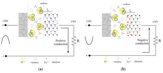
Figure 4.
Schematic views to demonstrate conduction and describe physical phenomena inside the Fe–Si steel/α-Fe2O3/graphite structure. (a) At positive conduction; (b) At negative conduction. Figure shows how exchange coupling at each interface depends on many species.
Figure 5 shows the current–voltage curve of each structure tested, in which it was observed that an Ohmic behavior for the α-Fe2O3/GR-1 interface occurs. Whereas, for α-Fe2O3/GR-2 and α-Fe2O3/GR-3 interfaces, the current–voltage curves follow a power–law relationship, I~Vm, with m = 1.5 roughly.
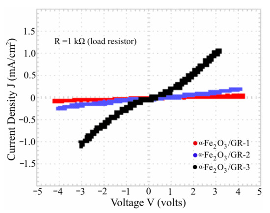
Figure 5.
Current–voltage plots in Fe–Si steel/α-Fe2O3/graphite structures to measure electrical conduction of three different interfaces.
Such power–law dependence is characteristic of space-charge-limited conduction (SCLC) at the interface [23]. Physical parameters were obtained from the plotted curves as follows. First, the activation energy, Ea, was found with the slope of each curve which crosses at the voltage axis. Second, because SCLC is limited by Arrhenius conductivity being dependent on temperature, then vacancies density, V, acting as defect sites in each graphite layer was estimated by µaVeρo = exp [−Ea·(2kBT)−1], where ρo = 40.57 × 10⁻⁶ Ω-cm as the resistivity of graphite [24]; kB is the Boltzmann constant; T is the temperature of the samples under test; and µa is the average mobility of charge carries flowing inside each graphite layer. Third, to determine how the charge carrier density is diffused at the interface, as the conducting channel, during each activation half-cycle from the sinusoidal voltage, the electrostatic length, le, was also estimated using empirical Poisson’s equation єoEa = en(le)210−4 to analyze conduction in materials [25], where єo is the dielectric constant in free space and n is the carrier concentration in absence of defects. Thus, using n = (eρoµa)−1 resulted in n = 6.16 × 1020 cm−3 in graphite.
Table 3 summarizes the finding conduction parameters where the quantity µaV was computed, confirming that V reduced from ~1015 to ~106 cm−3, which aligns with the growing number of disorderly stacked carbon sheets in the graphite samples. For all of the graphite samples, µa = 250 cm2/Vs was used [11]. Besides, phenomenological description related to the internal states at the α-Fe2O3/graphite interface, as a function the conduction polarity at each half-cycle of the sine wave, is given below:
Table 3.
Conduction parameters at the α-Fe2O3/graphite interface under alternating current injection.
3.3.1. Conduction at Positive Half-Cycle
In order to know how the α-Fe2O3/graphite interface acts as conducting channel at the positive electric field applied, a nonlinear diffusion of the charge carriers is caused through the interface and limited by attractive and repulsive electrostatic forces, where oxygen vacancies are acting as positive-charge trapping sites and the negative space-charge region, being the electrostatic length, le, results inside the graphite layer, as shown in Figure 4a. Therefore, change in the current density shown in the current–voltage plots results to be perturbed by exchange phenomena near the α-Fe2O3 surface.
3.3.2. Conduction at Negative Half-Cycle
By reversing the sine wave polarity, the negative electric field applied favors charge depleting from oxygen vacancies near the α-Fe2O3/graphite interface. Thus, a diffusion of charge carriers now is limited by charge accumulation inside the domain walls near the Fe–Si steel/α-Fe2O3 interface, because slight domain wall motion occurs due to the magnetostriction phenomena by native crystalline defects in the Fe–Si steel and positive space-charge region, being the electrostatic length, le, inside the graphite layer, as shown in Figure 4b. The Fe–Si steel/α-Fe2O3 interface acting as conducting channel allows the current flow to be influenced by charge accumulation near to the shallow domain walls of Fe–Si steel foil, but also by the energy magnitude of injected electrons from electrodes.
3.4. An Approach for Analog Computing Using the Fe–Si Steel/α-Fe2O3/Graphite Structure
The prototype architecture of Figure 6a, comprising one Fe–Si steel foil, one α-Fe2O3 thin-film grown on Fe–Si steel by thermal oxidation and one graphite layer, all being mechanically joined, was used to build a structure intended for mixed-signal signal processing. This was done in order to generate a output state whereby a particular integration of input signals must be reached, just as many interacting analog neurons in the brain do to process complex data sequences [26]. It is expected, nevertheless, that the Fe–Si steel/α-Fe2O3 interface will act as the source of nonlinearity, perturbing the charge carries motion at the α-Fe2O3/graphite interface when a DC supply voltage (VDC = 5 V) with the graphite layer is connected in series. Owing to this, it is possible to obtain weight states from point analog of view, which is useful, for example, in evaluating equivalent arithmetic values, as shown in the current–voltage plots of Figure 6b. In addition, the current–voltage plot when VDC = Null was included as reference to validate change of states.
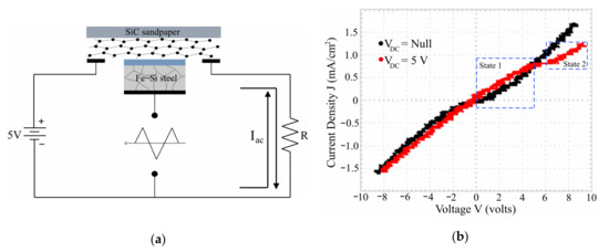
Figure 6.
Analog computing inspired by magnetostriction in Fe–Si steel and the disordered structure of the graphite layers. (a) Simpler prototype architecture for analog computing; (b) current–voltage plot shows two states of different conduction energy as possible arithmetic values.
In Figure 7, three modified bipolar-triangle signals were extracted from the load resistor R = 1 kΩ from the circuit of Figure 6a, whose average current magnitude was defined by Iac. As each signal contains different internal energy distributions, more weight states can be identified, being those dependent on the distributed resistance as a function the increasing magnitude of Iac of each graphite layer, labeled as GR-1, GR-2, and GR-3. In addition, a bipolar-triangle signal, fixed here of voltage amplitude ± 10Vpk, connected at the Fe–Si steel foil. All of which to produce the magnetostriction-induced conduction at the Fe–Si steel/α-Fe2O3 interface. The shape of the current signal extracted from the α-Fe2O3/Al interface alone when a bipolar-triangle signal is applied was also included as reference.
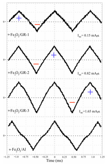
Figure 7.
Current signals measured from the architecture of Figure 6, where three different interfaces are evaluated. The α-Fe2O3/Al interface was included as reference to validate how energy distribution might be responsible of weight states.
Accordingly, the weight states, in terms of internal energy content in current signals, might define specific features of a physical, chemical and biological specimen from the analog-valued sensor response at variable bias voltage, VDC, as confirmed in Figure 6b.
Closer inspection shows that the energy distribution in the signals of Figure 7 varies with the change in graphite composition, where a fraction of positive-current signal (+) is broader when magnetostriction is pointing towards the α-Fe2O3/graphite interface, while it becomes a narrower fraction of negative-current signal (−) when magnetostriction is pointing away from this interface.
4. Discussion
Nowadays, digital architectures result in increased power consumption and temperature runaway, because billons of transistors operate under switching conduction to ensure that routines performed by a series of discrete steps become the needed algorithm solution. In addition, it is known that electric and thermal stresses during switching conduction of transistors cause limitations as coding faults when these are operating at higher speeds [12,19]. To improve reliability in digital systems, emergent schemes in recent years are generating renewed interest, whereby continuous growth of neuromorphic computing for bio-inspired data processing and hardware emulation of cellular building blocks are widely explored to perform analog-valued encoding [13]. However, a growing number of building blocks, difficulty to configure arbitrary connections between distant blocks of devices and scaling linearly with the size are some drawbacks in analog schemes.
Using the structure and conduction properties of Fe–Si steel and graphite might help enable the analog-valued encoding with advantages in operation, such as a reduced number of devices to avoid large connections and unstressed electrical conduction. Such properties will play a dominant role in the performance when energy loss-related resistive conduction of excited charge carries, and proximity effects (local temperature changes, magnetic ordering, electrostatic interactions, etc.) by magnetostriction and disorder effects, allow for adjustable exchange interactions at the surrounding interface in the α-Fe2O3-coupled Fe–Si steel/graphite structure. In addition, they will allow for reconfigurable action from the α-Fe2O3 oxide [15,27], being normally antiferromagnetic as a function of the structure ordering between Morin temperature (TM = 250 K) and Néel temperature (TN = 950 K), in which oxygen vacancies into their band gap (~2.2 eV) will be responsible of their nonlinear electrical conduction [28,29].
For instance, the results of Raman spectroscopy in the previous section highlight the following findings. (a) The level of defects in the GR-1 sample is small because the peak intensity of D band is negligible and the peak intensity ratios of 2D and G bands are very similar, thus this graphite layer is not defect free. However, GR-2 and GR-3 samples reveal strong disorder by possible intercalated accommodation of clay particles in the graphite lattice; (b) the D band is larger than the G band in the GR-2 sample, which means that there are more defects in sp2 hybridized-carbon atoms than the presence of stable layers. Whereas, the 2D band is higher and D band is lower than the G band in the GR-3 sample, which means that more phonon vibrational modes are excited and a growing number of layers are stacked; (c) the difference in FWHM of the measured D band (<70 cm−1) and 2D band (72 cm−1) for the GR-2 sample and that for the GR-3 sample (130 cm−1) implies that activation of the defects built-in graphite sheets will be slightly effected by local temperature changes, dependent on the proximity of randomly distributed defects; (d) magnetic ordering shown in the Fe–Si steel/α-Fe2O3 interface was understood by FWHM of the wide band from 550 to 800 cm−1 and the peak intensity ratio of 233.67 cm−1 (A1g) and 672.76 cm−1 (Eu) bands. This specifies that α-Fe2O3 corresponds to an oxygen-enhanced oxide with weak magnetostriction, which confirm that nonlinear diffusion of the charge carries will happen when α-Fe2O3 oxide becomes perturbed by interface forces near the Fe–Si steel surface, whereby randomly distributed charge in the interior of domain walls results.
Therefore, a theoretic approach for engineering the arithmetic processor where its internal architecture may be tailored from electrical conduction properties found in graphite and Fe–Si steel, mediated by α-Fe2O3, must include a stripe array based on distributed resistance of graphite layers, being it directly coupled to the α-Fe2O3 surface, as shown in Figure 8. Here, three graphite layers of different compositions must be assembled on silicon carbide (SiC) sheets, as in an earlier report [5]. The resulted analog device architecture could be configured to accumulate the weighted sum models of the inputs data through load resistor within the two following principles. First, variable voltage-valued data, applied as input signal and nonlinearly perturbed by magnetostriction induced at the Fe–Si steel/α-Fe2O3 interface, is possible using a linear ramp of different amplitudes as the activation signal. Second, modified pulses-valued data, applied as input signal, could be combined with the magnetostrictive signal produced at the interface and replicated in the load resistor. Both scenarios might be used to extract equivalent arithmetic values of many independent input states, as presented in Figure 8, with desired features when interconnecting load resistors in systems. For example, in resistor-capacitor (RC) circuits or complementary metal-oxide-semiconductor (CMOS) devices manufactured by silicon-based technology or emerging technologies [19,30].
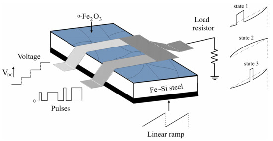
Figure 8.
Theoretic arithmetic processor, inspired by electrical conduction properties of Fe–Si steel and graphite, mediated by α-Fe2O3 oxide, to evaluate arithmetic values from weight states of the output signal.
5. Conclusions
An atypical solution for the renascent field of analog computing from recycling principle, and inspired by the hardware emulation of cellular building blocks, was attained by studying the special properties of materials, such as disorder in stacked sheets of graphite assembled on silicon carbide (SiC) and magnetostriction-induced electrical conduction at the Fe–Si steel/α-Fe2O3 interface. It was shown that fundamental tools, such as recycling practices and basic characterizing routes (e.g., Raman spectroscopy and current–voltage plots), were useful to conceive the functional architecture, which was established by change in composition of the graphite layers and the capability to perform conduction properties with Fe–Si steel, as well as their amenability to interfacing them with α-Fe2O3 oxide to integrate operating modes, such as reconfiguration for data encoding of multiple states.
Funding
This research received no external funding and the APC was funded by the author.
Institutional Review Board Statement
Not applicable.
Informed Consent Statement
Not applicable.
Data Availability Statement
Not applicable.
Acknowledgments
Thanks to Ramón Peña-Sierra for his earlier expertise on thermal oxidation, useful for the above-exposed study, and Miguel Galvan-Arellano for collecting the Raman spectrum data, both from SEES at the CINVESTAV-IPN, Mexico City.
Conflicts of Interest
The author declares no conflict of interest.
References
- Blomsma, F.; Brennan, G. The emergence of circular economy: A new framing around prolonging resource productivity. J. Ind. Ecol. 2017, 21, 603–614. [Google Scholar] [CrossRef]
- Maina, S.; Kachrimanidou, V.; Koutinas, A. A roadmap towards a circular and sustainable bioeconomy through waste valorization. Curr. Opin. Green Sustain. Chem. 2017, 8, 18–23. [Google Scholar] [CrossRef]
- U.S. Geological Survey, Mineral Commodity Summaries 2020: U.S. Geological Survey. 2020. Available online: https://pubs.usg.gov/periodicals/mcs2020 (accessed on 1 April 2021).
- Norgren, A.; Carpenter, A.; Heath, G. Design for Recycling Principles Applicable to Selected Clean Energy Technologies: Crystalline-Silicon Photovoltaic Modules, Electric Vehicle Batteries, and Wind Turbine Blades. J. Sustain. Metall. 2020, 6, 761–774. [Google Scholar] [CrossRef]
- Baca, R. Recovery of electronics waste to be converting into functional devices. MRS Adv. 2019, 4, 1067–1075. [Google Scholar] [CrossRef]
- Fogarassy, C.; Finger, D. Theoretical and Practical Approaches of Circular Economy for Business Models and Technological Solutions. Resources 2020, 9, 76. [Google Scholar] [CrossRef]
- Ouyang, G.; Chen, X.; Liang, Y.; Macziewski, C.; Cui, J. Review of Fe-6.5 wt.% Si high silicon steel—A promising soft magnetic material for sub-kHz application. J. Magn. Magn. Mater. 2019, 481, 234–250. [Google Scholar] [CrossRef]
- Hunday, J.; Cernik, M.; Hilinski, E.; Predmersky, M.; Magurova, A. Influence of chemistry and hot rolling conditions on high permeability non-grain oriented silicon steel. J. Met. Mater. Miner. 2006, 304, e620–e623. [Google Scholar]
- Dresselhaus, M.S.; Dresselhaus, G. Intercalation compounds of graphite. Adv. Phys. 2002, 51, 1–186. [Google Scholar] [CrossRef]
- Cotton, A.; Wilkinson, G. Advanced Inorganic Chemistry, 4th ed.; John Wiley & Sons: New York, NY, USA, 2008. [Google Scholar]
- Baca Arroyo, R. Graphite Intended for Green Engineering Developed by Noncontaminant Reverse Abrasion. Adv. Mater. Sci. Eng. 2016, 2016, 7016457. [Google Scholar] [CrossRef]
- Manganaro, G. Advanced Data Converters, 1st ed.; Cambridge University Press: New York, NY, USA, 2012. [Google Scholar]
- Zarcone, R.V.; Engel, J.H.; Eryilmaz, S.B.; Wan, W.; Kim, S.; BrightSky, M.; Lam, C.; Lung, H.-L.; Olshausen, B.A.; Philip Wong, H.-S. Analog coding in emerging memory systems. Sci. Rep. 2020, 10, 6831. [Google Scholar] [CrossRef]
- Zhao, X.; Du, Y.; Liu, Y.; Du, Z.; Yuan, D.; Liu, L. Magnetostrictive properties of the grain-oriented silicon steel sheet under DC-biased and multisinusoidal magnetizations. Materials 2019, 12, 2156. [Google Scholar] [CrossRef] [PubMed]
- Mohamed, A.Y.; Park, W.G.; Cho, D.-Y. Chemical structure and magnetism of FeOx/Fe2O3 interface studied by X-ray absorption spectroscopy. Magnetochemistry 2020, 6, 33. [Google Scholar] [CrossRef]
- Cabrera, N.; Mott, N.F. Theory of the oxidation of metals. Rep. Prog. Phys. 1949, 12, 163–184. [Google Scholar] [CrossRef]
- Caplan, D.; Hussey, R.J.; Sproule, G.I.; Graham, M.J. The effect of FeO grain size and cavities on the oxidation of Fe. Corros. Sci. 1981, 21, 689–711. [Google Scholar] [CrossRef]
- Baca, R. Extraction of hysteresis parameters in foil magnetostrictive composites. Results Phys. 2019, 12, 2066–2068. [Google Scholar] [CrossRef]
- Theis, T.N.; Wong, H.-S.P. The end of Moore’s law: A new beginning for information technology. Comput. Sci. Eng. 2017, 19, 41–50. [Google Scholar] [CrossRef]
- Ferrari, A.C.; Meyer, J.C.; Scardaci, V.; Casiraghi, C.; Lazzeri, M.; Mauri, F.; Piscanec, S.; Jiang, D.; Novoselov, K.S.; Roth, S.; et al. Raman spectrum of graphene and graphene layers. Phys. Rev. Lett. 2006, 97, 187401. [Google Scholar] [CrossRef]
- Lübbe, M.; Gigler, A.M.; Stark, R.W.; Moritz, W. Identification of iron oxide phases in thin films grown on Al2O3 (0 0 0 1) by Raman spectroscopy and X-ray diffraction. Surf. Sci. 2010, 604, 679–685. [Google Scholar] [CrossRef]
- Shim, S.-H.; Duffy, T.S. Raman spectroscopy of Fe2O3 to 62 GPa. Am. Miner. 2001, 87, 318–326. [Google Scholar] [CrossRef]
- O’Dwyer, J.J. The Theory of Electrical Conduction and Breakdown in Solid Dielectrics, 1st ed.; Clarendon Press: Oxford, UK, 1973. [Google Scholar]
- Pendrys, L.A.; Zeller, C.; Vogel, F.L. Electrical transport properties of natural and synthetic graphite. J. Mat. Sci. 1980, 15, 2103–2112. [Google Scholar] [CrossRef]
- Sze, S.M.; Ng, K.K. Physics of Semiconductor Devices, 3rd ed.; Wiley: Hoboken, NJ, USA, 2007. [Google Scholar]
- Kim, M.-K.; Park, Y.; Kim, I.-J.; Lee, J.-S. Emerging materials for neuromorphic devices and systems. iScience 2020, 23, 101846. [Google Scholar] [CrossRef] [PubMed]
- Mizuchima, K.; Kinno, T.; Tanaka, K.; Yamauchi, T. Strong increase of the effective polarization of the tunnel current in Fe/AlOx/Fe junctions with decreasing Fe layer thickness. Phys. Rev. B 1998, 58, 4660. [Google Scholar] [CrossRef]
- Blundell, S. Magnetism in Condensed Matter, 2nd ed.; Oxford University Press: Oxford, UK, 2008. [Google Scholar]
- Liao, P.; Toroker, M.C.; Carter, E.A. Electron transport in pure and doped hematite. Nano Lett. 2011, 11, 1775–1781. [Google Scholar] [CrossRef] [PubMed]
- Bishop, M.D.; Hills, G.; Srimani, T.; Lau, C.; Murphy, D.; Fuller, S.; Humes, J.; Ratkovich, A.; Nelson, M.; Shulaker, M.M. Fabrication of carbon nanotube field-effect transistors in commercial silicon manufacturing facilities. Nat. Electron. 2020, 3, 492–501. [Google Scholar] [CrossRef]


Publisher’s Note: MDPI stays neutral with regard to jurisdictional claims in published maps and institutional affiliations. |
© 2021 by the author. Licensee MDPI, Basel, Switzerland. This article is an open access article distributed under the terms and conditions of the Creative Commons Attribution (CC BY) license (https://creativecommons.org/licenses/by/4.0/).