1. Introduction
Thermoelectric generators (TEGs) exploit the voltage differential across n- and p-type materials when a temperature gradient is present, via the Seebeck effect, allowing for current to be driven through an applied electric load. TEGs are often utilised as energy harvesters powered by waste heat in the automotive, power, and personal electronic industries. In particular, flexible TEGs (f-TEGs) gained attention for the wearable technology sector, utilising the natural thermal gradient between the body (37 °C) and the surrounding environment (15–25 °C), powering low-power devices such as health monitors and sensors [
1,
2,
3].
Roll-to-roll (R2R) is a desirable manufacturing technique for flexible electronics that can be utilised for devices such as f-TEGs. Webs of flexible substrates are wound at high speeds, e.g., 10–500 m min
−1 from one roll, through processing chambers, back onto another roll. Multiple layers of a device can be deposited in sequential deposition steps within a single pass of the R2R [
4,
5,
6,
7,
8]. Physical vapour deposition (PVD) techniques, such as sputtering and thermal evaporation, offer high-quality and tuneable thin films and recently demonstrated promising R2R compatibility for high-throughput manufacturing of f-TEGs. To create patterned devices, flexography is an ideal PVD-R2R compatible process, offering high speeds (e.g., up to 180 m min
−1), and relatively low set-up costs compared to that of traditional ink-jet or gravure techniques [
4,
9].
Flexographic oil masking transfers oil from a stamp to the substrate to function as a mask. During deposition of thin films via PVD, the oil mask is simultaneously evaporated or ablated, removing the mask and leaving behind the patterned thin film. However, complete removal of the oil during this process is challenging, often with oil residue left behind, thus creating potential contamination and cleanliness problems for subsequent fabrication steps, possibly compromising the function of devices [
4,
10].
This paper proposes a novel approach to overcome this challenge by incorporating a linear electron beam (LEB) process into the PVD-R2R flexography process line. To obtain a suitably clean surface for deposition of subsequent device layers after electrode deposition by oil masking, an in-vacuum cleaning stage was deemed a fundamental processing requirement to progress and develop oil patterning for full multilayer device fabrication. For sputter deposited Cu and Ag as in ref. [
4], where oil was not removed, an iso-propanol wiping stage was used to remove oiled regions. However, an R2R compatible technique, linear electron beam irradiation (LEB), was implemented here to ablate residual oil and organics to cleanse the surface prior to semiconductor deposition. LEB sources for commercial R2R application were used for web precleaning and/or as a polymerisation source for organic films. In operation, an Electron beam is produced via a positively charged hollow cathode and collimated through a linear aperture with control of the magnetic field arrangement around the source. This produces both a sheet-like Electron beam and ionisation of the Ar process gas to generate plasma, directed at the moving web [
11]. Other high energy ablation techniques such as pulsed electron beams were used extensively for surface modifications from etching to recrystallisation or polishing of films [
12,
13].
The effects of the approach will be assessed in the form of a f-TEG, which consists of alternating n-type and p-type semiconductor thermoelectric strips connected in an S-like formation via electrodes. Firstly, aluminium electrodes are deposited via flexography allowing for the Electron beam cleaning technique to be reviewed. The effects of this Electron beam cleaning will be assessed in the form of multiple f-TEGs by subsequent deposition of thermoelectric materials by sputtering through a shadow mask. Optimisation of the particularly active thermoelectric materials of BiTe and BiSbTe or GeTe was extensively investigated within the group and through collaborators, however, with limited scalability via the use of shadow masked electrodes [
5,
6,
7,
14]. Here, we aim to successfully demonstrate the next required processing step for the realisation of continuous oil masking of the electrode to fabricate a full device architecture within a dynamic R2R system.
2. Results and Discussion
This work will implement LEB within a R2R process chamber as an in-line technique for surface cleaning following flexographic oil masking. Continuous R2R patterning is achieved by flexographic oil masking onto flexible substrates followed by deposition of materials, resulting in simultaneous oil removal, leaving behind the patterned deposited material. Three possible theories can be used to describe the oil masking mechanism: (i) radiative heating of the oil by the thermal deposition source increases the oil vapour pressure to produce an imparting and repelling vapour cloud from the oil mask surface to selectively prevent deposition [
10]; (ii) heat of condensation of the depositing material on the oiled regions vaporises the oil and ablates the depositing material, selectively preventing deposition; (iii) the depositing material is unable to nucleate on the oil surface and condenses elsewhere [
15].
f-TEGs will be used as device demonstrators to assess the viability of using LEB as a surface cleaning technique in an R2R environment. The fabrication steps are listed below:
- (1)
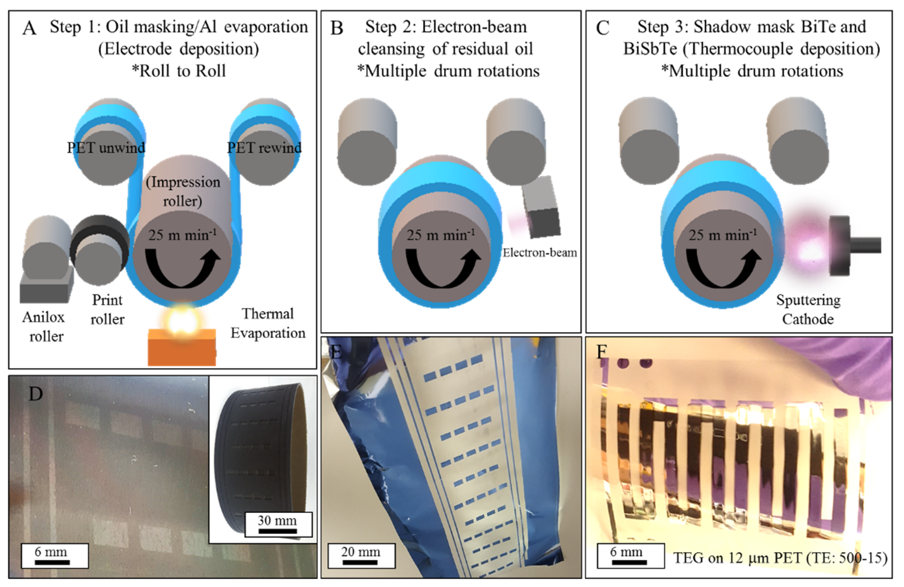
Aluminium electrodes are thermally evaporated using R2R flexographic oil masking (
Figure 1A). Aluminium is a commonly used electrode material.
- (2)
The Al electrode patterned substrate is cleaned via LEB for 0, 3, 5 or 15 min where the time quoted is the duration of time on the rotating drum vs. the actual exposure time to the Electron beam per rotation (
Figure 1B). The substrate chosen is a 12 µm (fully flexible) polyethylene terephthalate (PET), commonly used as a low-cost packaging film.
- (3)
Four pairs of thermoelectric strips are sputtered through a shadow mask (
Figure 1C). As the thermoelectric material performance is linked to operating temperature, BiTe and BiSbTe, which remain two of the more promising semiconducting materials operating in the low-temperature range up to ~100 °C, were selected for first tests, whilst a recently promising room-temperature compatible GeTe (p-type) material was selected for the second test to investigate material-oil compatibility [
3,
14,
16].
Figure 1.
Three-step methodology for producing scalable thermoelectric generators on flexible PET at substrate speeds of 25 m min−1. (A) Step 1: roll-to-roll Al electrode patterning by flexographic oil masking followed by Al thermal evaporation. (B) Step 2: removal of residual oil on PET by electron-beam irradiation. (C) Step 3: sputter deposition of thermoelectric semiconductors. (D) Printed oil pattern and nitrile print sleeve acquired from Phoenix Printing Plates Ltd. (E) Printed electrode section was removed from rewind roll. (F) Complete generator on pristine electrodes; TE:500-15. Nomenclature was assigned to manufactured TEGs to denote approximate semiconductor thickness in nm and Electron beam on-time, e.g., TE:500-15 to denote 500 nm and 15 min Electron beam cleaning time.
Figure 1D–F display photographs of each processing stage, including the printed oil mask (
Figure 1D) using a nitrile print sleeve (
Figure 1D inset), a section from the 25 m Electron beam cleansed electrode roll (
Figure 1E) and a completed four-pair, pristine, and operational TEG (
Figure 1F).
BiTe/BiSbTe f-TEGs, each containing four semiconductor pairs, were fabricated using R2R deposited electrodes with a 0 (TE:100-0), 15 (TE:100-15), and 60 min (TE:100-60) LEB cleaning step to remove masking out prior to active layer deposition. A f-TEG made from statically deposited electrodes through a shadow mask, in oil-free conditions, was also fabricated for reference (TE: 100-ShadowMask).
To determine the composition and distribution of the deposited active materials (BiTe and BiSbTe) and to assess the impact of the cleaning step, we used Energy Dispersive X-Ray Spectroscopy (EDX). To quantify remaining masking oil from the patterning stage through to device fabrication, fluorine quantities were assessed within the Al electrode and through/below the semiconductor strips by EDX as the techniques electron beam readily reaches depths of severely microns, therefore beneath the ~100 nm Al layers here [
17]. Scanning Electron Microscopy (SEM) (at micron scale) and optical microscopy (micro scale) were each used to image the morphology of the surface. High-resolution compositional analysis was investigated by X-ray Photoelectron Spectroscopy (XPS) which enabled surface specific (1–10 nm) assessment of any reaction that occurred between masking oil, fluorine, and the aluminium electrode. Finally, the electronic performance of active materials was assessed by 4-point probe for resistivity, work function by Kelvin Probe, and Seebeck performance/power generation of devices by applying a temperature gradient across the device and measuring output through a high precision multimeter. A detailed account of each technique and parameters used can be found in the methodology section.
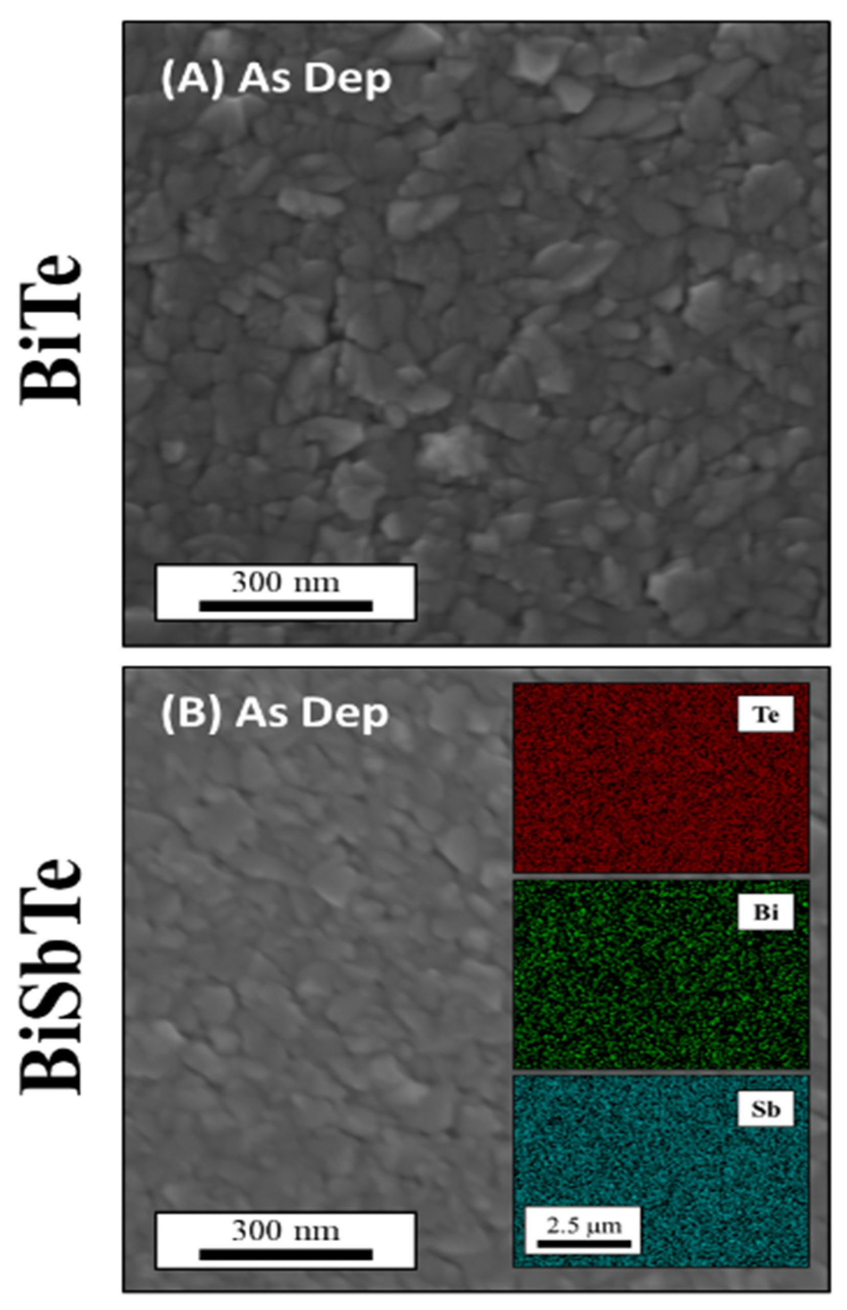
The sputtered semiconductor layers showed the following characteristics on deposition: (i) the composition, measured from EDX, was shown to vary slightly compared with that of the target for both materials (
Table 1). Preferential sputtering effects can cause variation in composition from sputtering target to deposited coating [
18]. SEM imaging of both films showed a granular morphology with features on an approximately 100 nm scale (
Figure 2A,B).
- (a)
LEB Irradiation of Spin Coated Oil (As a proxy methodology for determining oil removal rate)
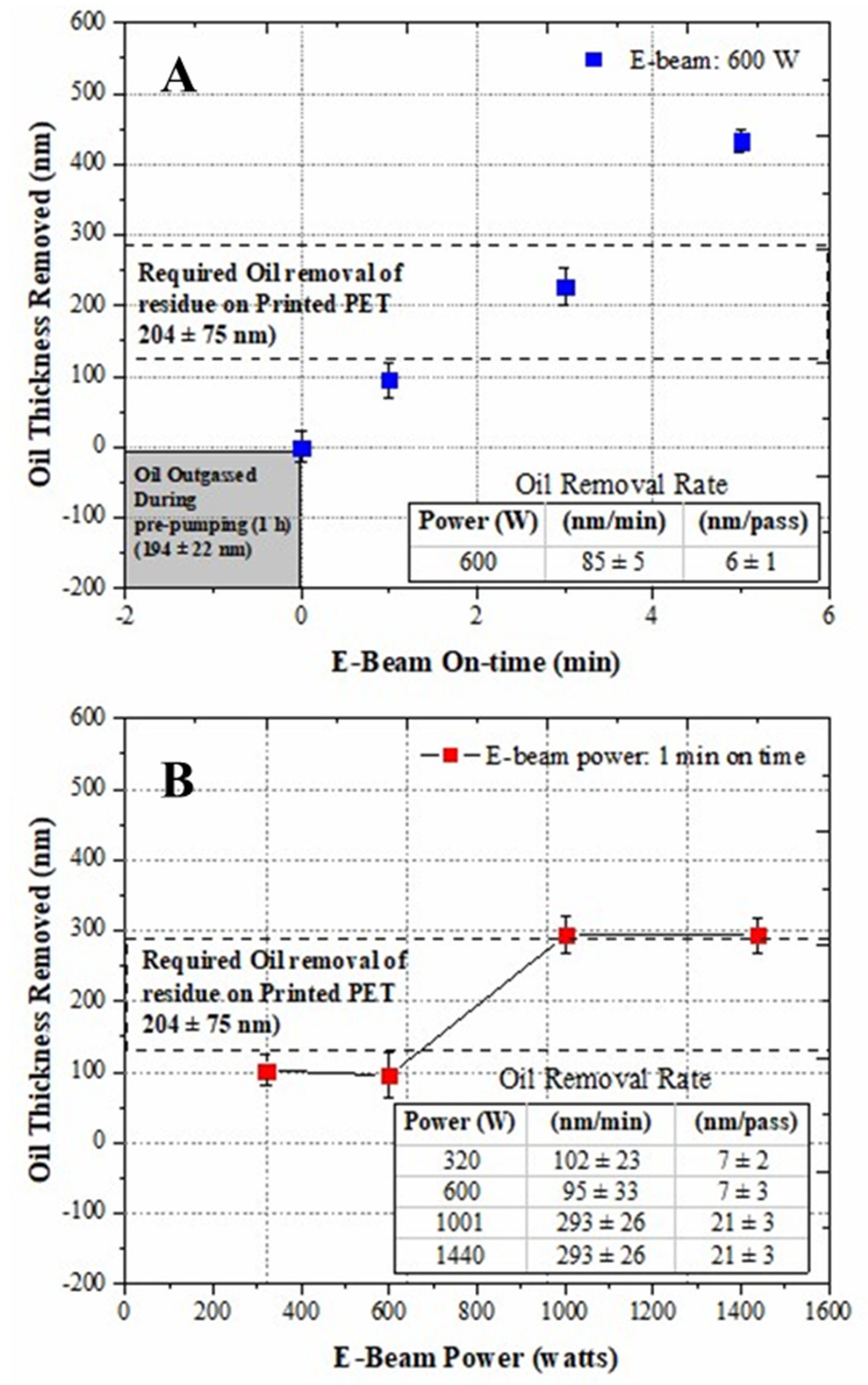
To optimise the LEB radiation step, oil was spin coated onto a glass cover slip, where a minimum thickness (determined by mass) of the oil layer was achieved at ~660 ± 110 nm. These films were then Electron beam irradiated for 1, 2, and 5 min at 600 W (
Figure 3A). A linear relationship suggested an oil removal rate of 85 nm min
−1 or 6 nm pass
−1. Electron beam power was varied from 320, 600, 1000, and 1440 W (
Figure 3B) to increase the oil removal rate to 293 nm min
−1 or 21 nm pass
−1. Notably, no variation in Electron beam performance was observed between 320 and 600 W or 1000 and 1440 W. These measurements give an indication of the thickness of residual oil (following a deposition process in which much of the printed oil is removed) that could be removed by a post-deposition Electron beam treatment.
The LEB effects on the Al electrodes were investigated via sheet resistance measurements, before and after 15 min of electron beam irradiation at 600 W (the conditions selected for f-TEG fabrication). It was confirmed that electrode resistivity increased only modestly, with the as-deposited Al exhibiting sheet resistance of 0.97 ± 0.03 × 10⁻⁷ Ω·m compared to 1.14 ± 0.04 × 10⁻⁷ Ω·m after radiation.
- (b)
LEB Irradiation of R2R printed Oil
Based upon the results from the static LEB optimisation and the beam being most stable at 600 W over a prolonged period, a 600 W LEB step was incorporated into the fabrication of f-TEGs. f-TEG properties are investigated here to assess how the LEB cleanings step impact device performance.
The oil thickness used for this R2R Al masking step was measured to be 204 ± 74 nm, indicating 3–5 min LEB process should result in a clean film even if no oil were removed during deposition of the Al. Nomenclature was assigned here to manufactured TEGs to denote approximate semiconductor thickness in nm and electron beam on-time, e.g., TE:100-15 to denote 100 nm and 15 min electron beam cleaning time.
TE:100-0 did not have an LEB cleaning step and is visually marred by remaining residual oil left behind after the electrode process (
Figure 4). This leads to an exfoliated morphology with porosity and cracks forming within the BiTe/BiSbTe strips that were sputtered after the electrode step, likely caused by over-coating onto oil. Similar findings were observed for sputtered Cu and Ag on oil masks [
4].
Based upon the static LEB study above, 3 and 5 min LEB radiation steps were expected to result in a full oil removal for the oil films deposited via R2R on PET. However, visual observation of the f-TEGs following electron beam irradiation for 3 and 5 min clearly displayed the effects of remaining masking oil similar to
Figure 4, suggesting the oil mask transfer possibly resulted in inhomogeneous oil layers, with the oil film exhibiting areas much thicker than 204 nm, or that LEB treatment of a partially metallized film provides less rapid cleaning. When the cleaning time was further increased to 15 min (TE:100-15), defect-free f-TEGs were achieved as shown in
Figure 4.
A total of 24–26 at% fluorine was measured from an area of the semiconductor deposited without an electron beam cleaning step, compared to 2% for the semiconductor deposited onto the 15 min LEB cleansed surface (
Table 2). The Al electrodes were measured by EDX to contain 6–7 at% fluorine in both the as-deposited and 15 min LEB irradiated devices. As Al was deposited onto unmasked regions only, and as they are the same for the cleaned and uncleaned specimens, this finding suggests that the masking fluorinated oil cloud evaporating from the surface during Al deposition possibly reacted or became trapped within the condensing Al electrode. This occurrence was previously found and assessed in ref [
4] where Al–F, Al–O, and metallic Al–Al species were found by XPS depth profiling through the thickness of the layer (for which the surface was saturated with fluorine of ~62 at%) [
4]. The f-TEG device here was completed in two stages prior to active material deposition: (1) R2R oil patterning and electrode deposition (single pass and taken up by the rewind roller), followed by (2) remounting of the electrode coated substrate onto the web for multipass oil cleaning. This leads to an alternative explanation for fluorine found within the electrode. Whereby, residual oil spread over the electrode as the Al electrode coated web passed over the idler rollers and was rewound onto the rewind roller during the single pass R2R process. Subsequent diffusion resulted in through-thickness fluorine contamination of the Al electrode. Future development work will aim to achieve single pass in-line oil patterning and electron beam cleansing.
XPS, which typically probes 5–10 nm in depth, was previously assessed for uncleaned electrodes in ref [
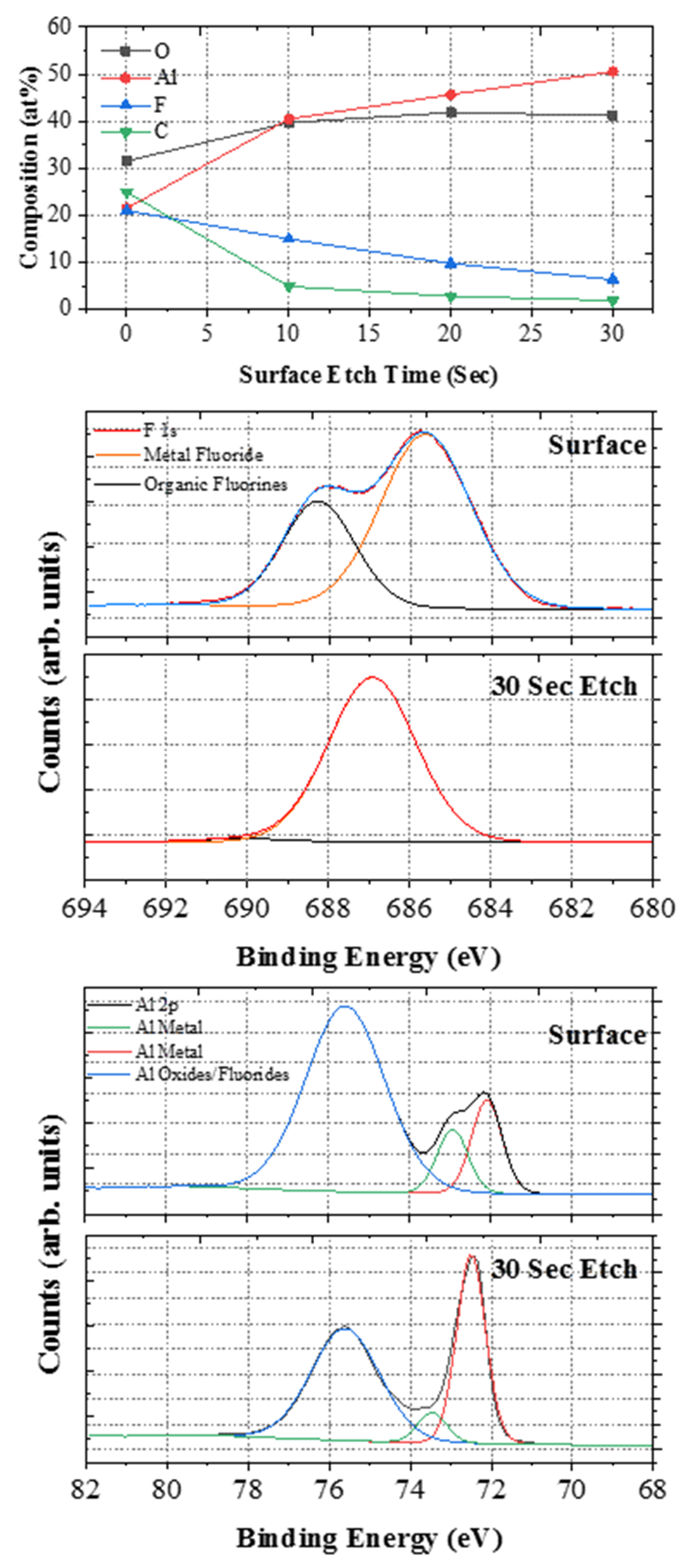
4]. XPS of Al surfaces following 15 min LEB after deposition were analysed here. Crucially, surface oil residue remained despite electron beam cleaning protocols, appearing to remove the bulk of oil residuals decreasing from 62 at% for uncleaned electrodes [
4] vs. 20 at% observed here. A fluorine reduction from 20–5 at% was found between the surface and the subsurface layers following ion depth etching for 30 s. A high-resolution scan of the F_1s (
Figure 5) showed photoelectron emissions at 685.5 and 688.2 eV, associated with metal fluoride (Al–F) and organic fluorine, respectively, and attributed to fluorinated oil compounds on the surface. The Al_2p contained peaks associated with Al–O or Al–F and metallic Al. Detection of the organic fluorine peaks with Al-F and metallic Al peaks suggested that only a thin (<10 nm) or incomplete residual oil layer remained to allow detection of the metallic/Al–F electrode beneath. Following a 30 s etch for depth profiling, the organic fluorine disappeared in the F_1s spectra whilst components associated with metallic Al increased in relative intensity compared to Al–O and Al–F which remained present. This confirms the reactivity of masking oil with aluminium vapour during deposition, as seen previously [
4].
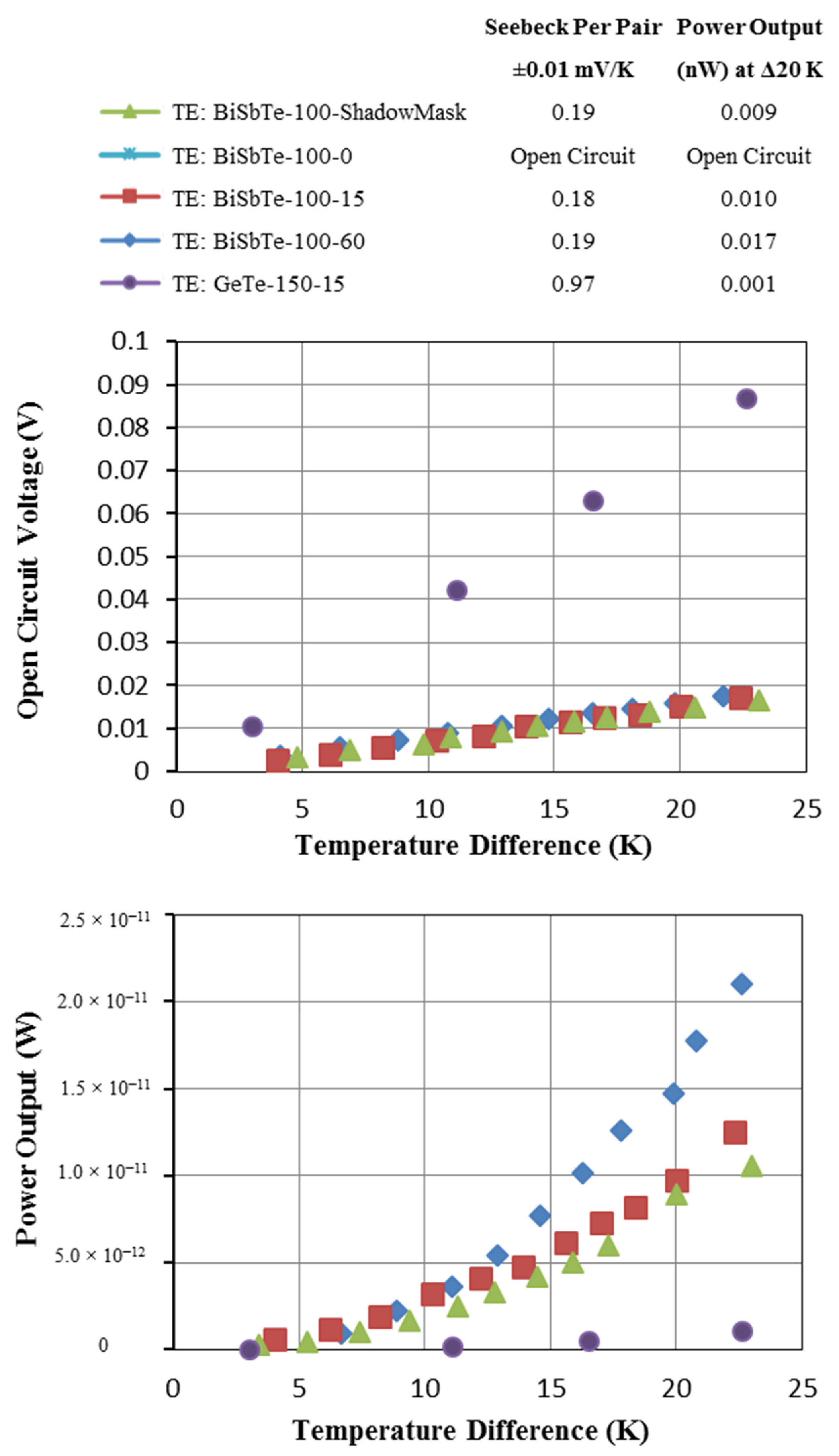
Seebeck coefficient and power generation were measured within 1 h of f-TEG manufacture. As presented in
Figure 6, uncleaned surfaces (TE:100-0) showed no power output, open circuit behaviour. Where electrodes were cleaned (TE:100-15 and TE:100-60), Seebeck per pair is comparable to the reference f-TEG manufactured using the oil free shadow masked electrode (TE:100-ShadowMask), all exhibiting S ~ 0.19 mV K
−1. The power output of these f-TEGs at ΔT = 20 K (conventional operating point near to room temperature for wearable devices) [
19] are also similar with P ~ 0.01 nW (TE:100-15 and TE:100-ShadowMask) and increased slightly for TE:100-60 to P ~ 0.02 nW.
f-TEGs were remeasured +3 days after manufacture and both TE:100-60 and TE:100-15 exhibited open-circuit behaviour. Upon further inspection at the semiconductor/electrode interface, devices demonstrated poor or no ohmic contacts and large variations in IV curves. This occurrence may were attributed to poor adhesion between the semiconductor and electrode, reaction with atmosphere as these were uncapped, or diffusion of fluorine through the Al layer; an effect reported previously by Stuart et al. [
4].
Work functions of uncleaned oil mask and shadow mask deposited Al electrodes were measured as 4.21 ± 0.05 and 4.14 ± 0.07 eV. To confirm compatibility at the layer interface, BiTe and BiSbTe were deposited on top of 15 min LEB cleaned electrode patterns and exhibited work functions of 4.71 and 4.68 eV, respectively (
Table 3). This is in good agreement with BiTe (4.65 ± 0.05 eV) and BiSbTe (4.61 ± 0.06 eV) deposited on clean PET which was never exposed to any oil steps.
To investigate the masking oil compatibility with other thermoelectric materials, a f-TEG with BiTe/GeTe layers of 150 nm thick was fabricated with Al R2R deposited electrodes followed by a 15 min LEB cleaning step (TE: GeTe-150-15). BiTe/GeTe recently demonstrated R2R high-throughput compatibility, and good thermoelectric performance based upon GeTe’s potential as a superior p-type TEG material [
14]. Following the R2R flexographic deposition of Al electrodes and a 15 min LEB cleaning step, BiTe and GeTe were statically consecutively sputtered through a hard shadow mask. The Seebeck and power output can be seen in
Figure 6, where TE: GeTe-150-15 exhibited a Seebeck per pair of 0.97 mV K
−1 and a power output of 0.9 pW at ΔT = 20 K. The BiTe/GeTe f-TEG in this work demonstrates a Seebeck coefficient that is over 5× higher than our BiTe/BiSbTe f-TEG made using the same Al flexographic and LEB cleaning steps. This can be attributed to GeTe’s superior thermoelectric behaviour [
20]. However, when looking at the power output, the BiTe/GeTe f-TEG in this work demonstrated a power output one order of magnitude lower than BiTe/BiSbTe. This could be attributed to GeTe’s high electrical resistance when deposited at room temperature, as indicated by the much higher output power of 1.8 nW at ΔT = 20 K of the BiTe/GeTe f-TEG in [
14], in which the thermoelectric materials were deposited onto a substrate held at 250 °C.
The BiTe/GeTe f-TEGs were measured again +2 months after fabrication and the electrode/TE interfaces were found to still demonstrate ohmic conduction, unlike the BiTe/BiSbTe which were unmeasurable after +3 days. Whilst they were still performing as a TEG, they did exhibit reduced Seebeck (0.65 mV K−1 per pair) and power output (0.3 pW at ΔT = 20 K), most likely due to reaction with the masking oil that the BiTe/BiSbTe also demonstrated. This demonstrates the reaction between the masking oils and the materials used in the process line can be reduced by selecting appropriate combination of mask and deposited material to reduce the effect on performance of deposited materials, resulting in improved, more stable device performance.
High-speed vacuum printing of thermoelectrics at low cost onto flexible films represents a considerable step forward for affordable commercialization of thin-film TEGs. By future stacking optimized thin-film modules, hundreds of layers will produce usable energy outputs. The output energy density of these modules vs. current Peltier devices will be of future importance. The authors. Tao et al. and Morgan et al. demonstrated considerable progress in other publications to optimize chalcogenide-based devices on the lab scale [
5,
6,
7,
14]. Significant research and development are still required for industrialization. The progress presented here begins to bridge the gap between lab scale optimization and continuous high-volume production.
3. Conclusions
Al electrodes were deposited by selective vacuum metallization using a single-pass, 25 m min−1, R2R patterning based on flexographic printing of Krytox® 1506 oil as a mask during continuous circuit manufacture. Flexible TEGs on 12 µm PET for operation in wearable generators were constructed by subsequent deposition of Bi0.56Te0.44 and Bi0.11Sb0.30Te0.49 through a shadow mask to prove principle of multilayer device fabrication using an oil masking stage. Residual oil on the sample during deposition of active thermoelectric layers led to porosity, cracking, and an exfoliated type morphology attributed to over-coating of remaining oil in masked regions.
A R2R electron beam irradiation processing step ablated oil residue prior to thermoelectric deposition, thereby successfully removing remaining oil to produce an unaffected morphology. Semiconductors were deposited to 99/96 nm for device fabrication requiring 42 drum rotations with power factors of 1.869 and 0.007 × 10⁻⁴ W/mK2 for BiTe and BiSbTe, respectively. However, fluorine remained present in quantities of 6 and 5 at% (EDX and XPS, respectively) within the electrode structure as an Al–F compound, whilst fluorine detected on oil-masked PET regions reduced from 24–26 at% (uncleaned) to 2 at% detected through the active layer after 15 min electron beam cleansing. Despite Al-F contaminates, devices were compared with shadow masked electrodes (no oil condition) which had similar work functions (4.21 and 4.14), comparable Seebeck coefficients (0.018–0.20 mV/K per pair), and power generation (0.009 and 0.017 nW), suggesting that device performance was minimally impaired. Critically, devices using oil-masked electrodes were remeasured 3+ days post-fabrication after storage in ambient conditions and were dysfunctional, which was attributed to diffusion of organic elements such as fluorine towards the interface. Finally, BiSbTe was replaced with GeTe, leading to a 5× increase in Seebeck coefficient and an order of magnitude for reduction in power factor, which was attributed to expected high resistance during room temperature deposition of GeTe. Material compatibility was improved using GeTe as the device remained functional 2 months post-fabrication.
Whilst challenges remain, work here showed for the first time (i) a R2R-compatible oil cleansing method for future multilayered device fabrication via oil patterning; (ii) ability to fabricate a functional BiTe/BiSbTe TEG using oil-masked electrodes manufactured at substrate speeds of at 25 m min−1; and (iii) improved stability in BiTe and GeTe TEGs using oil-masked electrodes.
