Article

Effect of Plating Current Density on the Ball-On-Disc Wear of Sn-Plated Ni Coatings on Cu Foils

1
Department of Materials Science and Engineering, Ajou University, Suwon, Gyeonggi 16499, Korea
2
Department of Energy Systems Research, Ajou University, Suwon, Gyeonggi 16499, Korea
*
Author to whom correspondence should be addressed.
Coatings 2021, 11(1), 56; https://doi.org/10.3390/coatings11010056
Submission received: 9 December 2020 / Revised: 31 December 2020 / Accepted: 31 December 2020 / Published: 6 January 2021
(This article belongs to the Special Issue Selected Papers from the K-TRIB2020)

Abstract

:
Metallic and alloyed coatings are used widely in several decorative and technology-based applications. In this work, we selected Sn coatings plated on Cu substrates for joining applications. We employed two different plating baths for the fabrication of Sn and Ni coatings: acidic stannous sulfate for Sn and Watts bath for Ni layer. The plating current densities were varied from 100–500 mA/cm2. Further, the wear and friction behavior of the coatings were studied using a ball-on-disc apparatus under dry sliding conditions. The impact of current density was studied on the morphology, wear, and coefficient of friction (COF) of the resultant coatings. The wear experiments were done at various loads from 2–10 N. The sliding distance was fixed to 7 m. The wear loss was quantified in terms of the volume of the track geometry (width and depth of the tracks). The results indicate that current density has an important role in tailoring the composition and morphology of coatings, which affects the wear properties. At higher loads (8–10 N), Sn coatings on Ni/Cu had higher volume loss with a stable COF due to a mixed adhesive and oxidative type of wear mechanism.

1. Introduction

With the advancement of portable microelectronic devices with high multifunctionality, further improvement of their life cycles and reliability is required. Electronic components are very sensitive to the surrounding environment, unwanted whisker outgrowths, cyclic wear, oxidation, and corrosion fatigue during insertion and withdrawal of separable components over a longer time interval. These undesirable changes in the conducting properties occur due to various reasons, such as poor wettability and strength of interconnections, compressive stresses buildup in the coating-substrate couple due to the surface chemistry, and the presence of organic impurities, which outgas during reflow procedures [1,2,3]. Therefore, the surface protection of microelectronic components and devices is in great demand. The surface modification of the electronic substrates and components can be achieved by several coating techniques: for example, physical vapor deposition, chemical vapor deposition, spray coating, electrochemical deposition, sol-gel, or laser ablation techniques [4,5]. Most of these techniques require precise control of the environment, use of expensive equipment, and well-trained operators to perform the job. All these requirements make the whole process extremely expensive and restrict further commercialization. In contrast, electrochemical methods are the simplest and most economical coating technologies for the protection of microelectronic circuits and devices [6,7]. Electrochemical techniques, such as electrochemical plating, have been used widely to plate electronic substrates, high strength thermal barrier coatings, and decorative applications [8,9]. A lot of developments in the field of electroplating have taken place over the years. Advanced pulse plating techniques utilize pulsed current (PC) to produce high instantaneous current density for the deposition of diverse nanostructures and composite coatings [10,11].
Nickel plating has already been used in semiconductor devices to protect copper conductors from external corrosion and thermal shock for efficient mechanical and electrical continuity among various circuit components in printed wiring boards (PWBs) [12,13]. Nickel plating on conducting substrates acts as an excellent diffusion barrier to unwanted Sn whisker growth on electronic components [14]. When Ni is alloyed with Sn, the resulting alloys can be applied to several applications, including surgical equipment, watch parts, press-fit connectors, and microwave connectors, due to their good anticorrosion properties. Ni–Sn alloys have been used over PWBs as etch-resistant coatings [15]. Ni–Sn alloys have a high resistance to oxidation and high hardness (6–7 GPa), which makes them a potential alternative to chromium coatings in automotive and electronics accessories. Recently, Ni–Sn alloys have also been investigated for the anode material in lithium-ion batteries [16].
Ni- and Sn-based electrodeposits are mostly produced from either electroless or electroplating methods [6,12,13]. Compared to direct current plating, PC plating has been widely used for Ni plating due to the various benefits, such as high uniformity, density, and tunability of grain size [5,6]. The surface characteristics of the resultant coatings rely on efficient parametric control, such as current density, pH, plating bath composition, pulse shape, duty cycle, and frequency [17]. Among these parameters, current density is believed to be one of the most important parameters to control the surface morphology and deposit stresses in the coatings. Higher current density causes a buildup of higher overpotential, which favors the nucleation process; however, it also raises the inherent evolution of hydrogen gases in the bath, which further may affect the porosity levels in the coating [18,19,20]. Therefore, microstructural tuning of the coating through PC plating requires knowledge of the microstructure and property-type relations of the deposits.
In this study, we developed Ni–Sn coating on Cu substrates by PC plating using acidic Sn and Watts-type Ni baths. Acidic baths have a mid-range pH and do not dissolve the photoresists on the electronic substrates, unlike the high pH of (~14) alkaline baths. Acidic baths contain various complex chemicals for surface modification and improved alloying and alleviate the deposit stress. Acidic baths are widely used because of their key role in bright and shiny surface finishes, but they need efficient waste disposal systems [17]. Further, Ni–Sn alloys have been used for a variety of electronic and automotive parts but without enough studies on the cyclic ball-on-disc wear and friction properties of Ni-plated Sn alloys. Therefore, we attempted to study the influence of current density on the morphology, roughness, thickness, hardness, and wear behavior of Sn-plated Ni on Cu foils for microelectronic contact applications.

2. Materials and Methods

2.1. Plating Bath

All the chemicals used were of reagent grade and were obtained from Sigma-Aldrich, St. Louis, MO, USA (99.9% purity). The plating bath chemicals and their nominal compositions are shown in Table 1. For Ni, we used a Watts-type electrolyte (pH = 4.3), while for Sn we used an acidic sulfate bath (pH = 0.9) (Table 1). The electrolytic bath was prepared in de-ionized water by dissolving the tabulated chemicals. The solution was kept stirring until the various salts got dissolved out completely. The electrolyte bath temperature was maintained at 44 ± 2 °C and 30 ± 2 °C for Ni and Sn electroplating, respectively. The Ni was plated at 300 mA/cm2, while the Sn was plated at various current densities varying from 100–500 mA/cm2. Other conditions were the same for both types of plated coatings. The thickness of the Ni film was 30 µm.

2.2. Plating Cell

Three-electrode cell geometry was used to perform the electroplating experiments. We employed a platinum foil as the counter electrode, while a Cu foil (25 × 25 × 2 mm3, 99.9%) was used as a working electrode. Ag/AgCl saturated with 3 M KCl was chosen as the reference electrode. Before electroplating, the Cu foil was subjected to metallographic polishing with SiC papers #400, #800, #1200, #1500, and #2000, up to 3 µm diamond paste. The prepared Cu substrate was further rinsed with distilled water, cleaned with alcohol, and mounted in an epoxy resin. Diluted 10% H2SO4 was used to clean the surface of Cu for a few seconds to remove the oxidizing layer. Epoxy resin acted as an insulator and protected the unexposed copper surface against corrosion. Nickel and copper were further applied for anticorrosion contact applications.

2.3. Plating Experiment

The electroplating experiment was performed using an EPP-4000 electrochemical pulse plater (Biologic Science Instruments, Seyssinet-Pariset, France). The experimental arrangement is shown in Figure 1. The EPP-4000 instrument provided a rectangular current waveform of definite pulse on and off cycles, as shown in Table 1. The current/potential curves were recorded by a personal computer attached to the EPP-4000.
The plating bath was continuously stirred at 300 rpm over a hot plate. The Sn coating thickness was estimated from the mass gain at the cathode and density of the coating material given by [5,6]:
( Deposit   thickness P l a t i n g   t i m e ) =   ( C u r r e n t   d e n s i t y   × CCE × ECE D e p o s i t   m a t e r i a l   d e n s i t y )
where ECE and CCE are electrochemical equivalent and cathodic current efficiency. CCE is given by the ratio of mass gain of metal at the cathode and the mass deposited according to Faraday’s laws of electrolysis [6]. The mass gained at the cathode was measured by a Sartorius physical balance with an accuracy of 0.01 mg. The roughness of the coatings was determined by a Veeco Dektak 150 surface profiler (Veeco Instruments, Tucson, AZ, USA). The roughness measurements were done across the cross-section of length 2000 µm at a speed of 66.66 µm/s. A total of five roughness measurements were recorded for each sample.

2.4. Microstructural Investigations

The structural evolution of the final coatings was studied by a benchtop X-ray diffractometer (XRD, Rigaku Miniflex, Tokyo, Japan) with Cu Kα radiation operating at 30 mA and 40 kV. The specimens were scanned from 30° to 80° at a rate of 0.05° s−1. The phase components were identified by the standard database using MDI/JADE software (Version: 9) [21,22,23]. The microstructure of the coatings was examined in a scanning electron microscope (SEM-4800S, Hitachi, Tokyo, Japan) operating at 20 kV. The compositional analysis of the coatings was done by an energy-dispersive X-ray spectrometer (EDS) detector connected to the SEM machine.

2.5. Mechanical Tests

The microhardness of the coatings was determined by a HM220 Vickers microhardness tester (Mitutoyo, Kawasaki, Japan). The selected loading force was 25 gf for a duration of 20 s. A total of five measurements were recorded at different locations and the average value of the microhardness was reported for each condition.

2.6. Tribological Tests

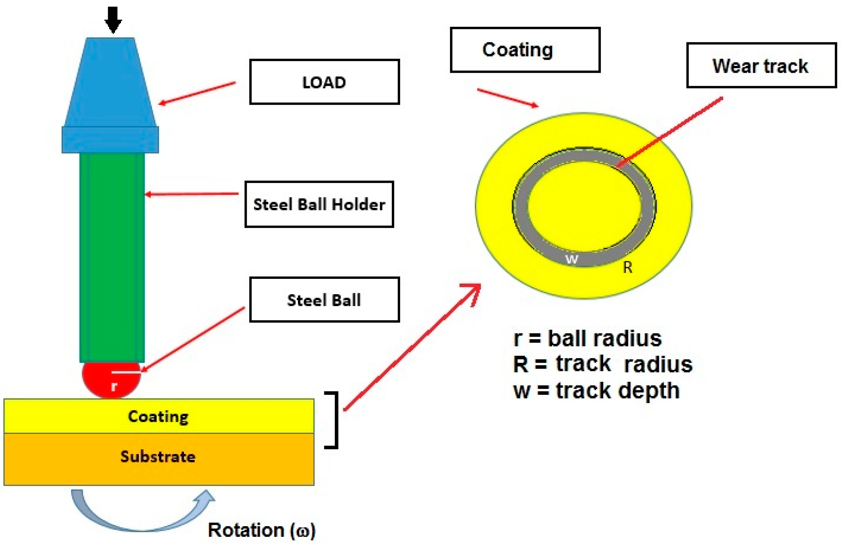
The wear tests on the coatings were conducted using ball-on-disc geometry (Ducom Tribometer, Bangalore, India) according to ASTM standards [24], as shown in Figure 2.
The wear test conditions are given in Table 2. The selection of parameters was done based on metallic coatings applied for electrical contact applications—for example, Cu-, Sn-, and multilayered Cu–Ni–Sn-based coatings [25,26]. We made Cu blocks of 25 × 25 × 2 mm3 size with 30 µm Ni and 30–55 µm Sn for wear tests depending upon the current density and thickness of Sn.
The wear loss was calculated by a Veeco Dektak 150 surface profiler from the equation [27]
V = 2 π R ( r 2 s i n 1 ( w 2 r ) ( w 4 ) ( 4 r 2 w 2 ) 0.5 )
The symbols r, R and w ae ball radius, tack radius and tack depth, respectively. Considering the wear volume, the wear factor (K) was determined by the equation [28,29,30]
K = V NL   ( mm 3 · N 1 · m 1 )
where N is the applied normal force, L is the sliding distance, and V is the wear volume loss. The coefficient of friction (COF) was given by the normal reaction force divided by the corresponding normal load and was automatically calculated by the ball-on-disc machine.

3. Results and Discussions

3.1. Phase Evolution

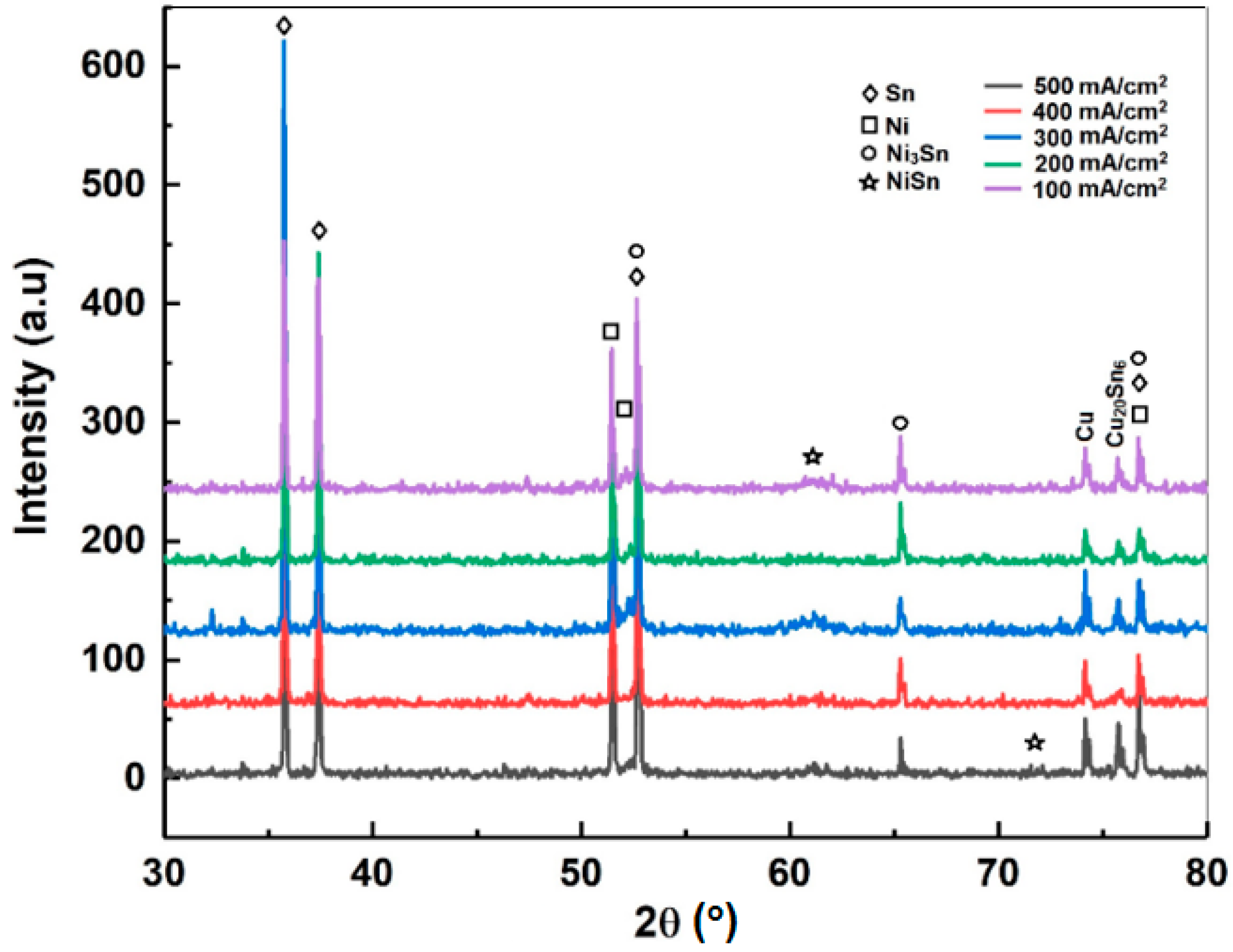
The resultant coatings were characterized for their phase evolution as shown in Figure 3. The various peaks were matched with the standard powder diffraction files—i.e., JCPDS File 04-0673 (for β-Sn), 01-1260 (for Ni), and 35-1362 (for Ni3Sn intermetallic compounds (IMCs))—that may have come from the adherent layers of the substrate. The Cu20Sn6 IMCs were formed in the coatings because Sn–Cu atoms diffused at the grain interfaces and precipitated out. All the samples showed a similar trend, which is consistent with a few research reports [31,32].
The NiSn phase was identified at 63.58° and 72.65°, and the peaks at 74.20° were assigned to the Cu substrate (JCPDS file 04-0836) [31,32]. The metastable NiSn phase had a hexagonal structure which stabilized to a Ni3Sn2 phase. The additional Sn atoms were embedded into the alloy, thereby modifying the lattice constants, as noticed by Rooksby [32].

3.2. Morphology

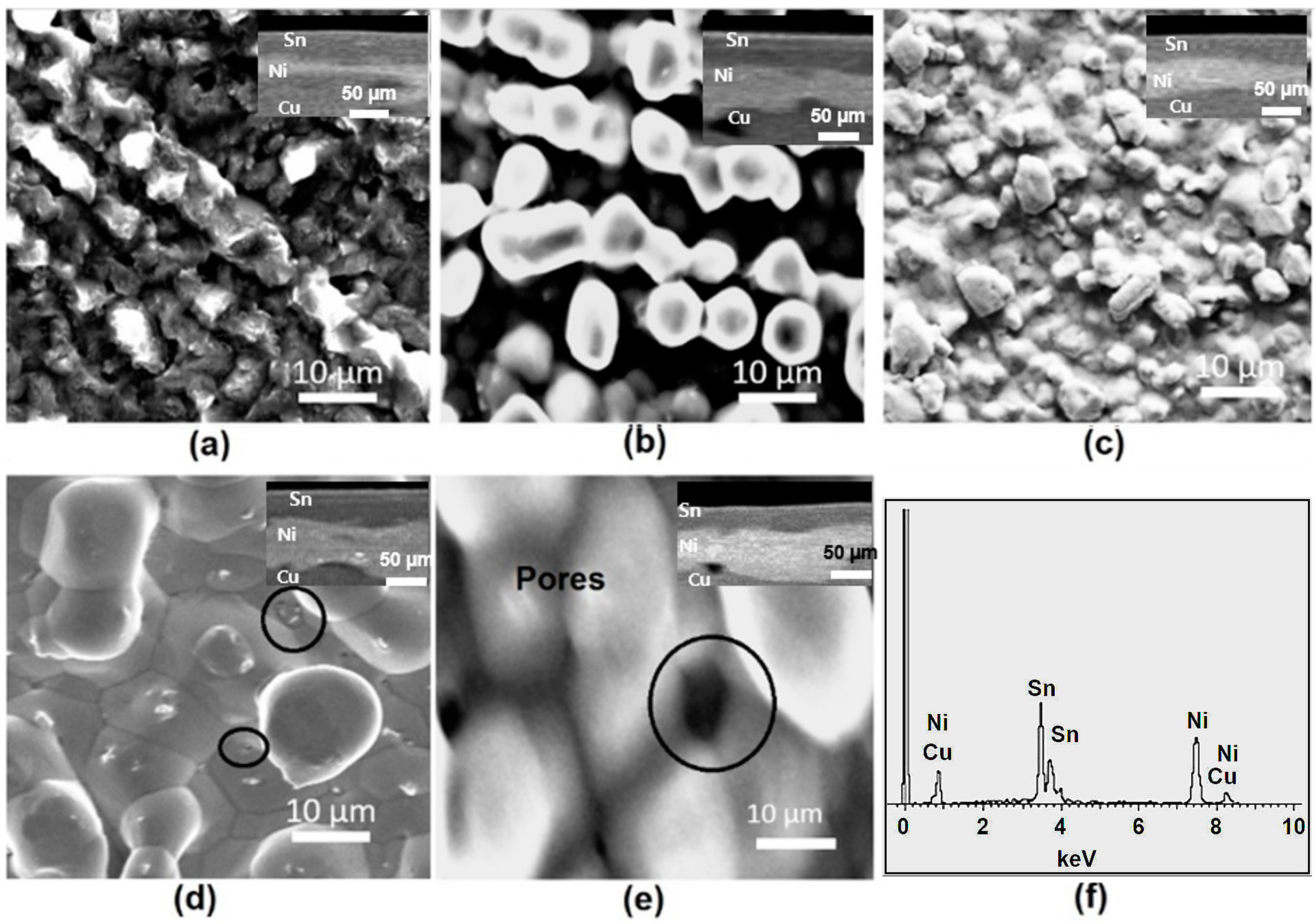
The surface morphology of the coatings is shown in Figure 4. The morphology was globular and non-uniform at lower current densities, i.e., 100–200 mA/cm2. The cathode coverage improved with an increase in current density up to 300 mA/cm2. The grain size was also reduced at 300 mA/cm2. However, the grains increased in size, and some pores were noticed emerging from the coatings at higher current densities, i.e., 400–500 mA/cm2. This can be attributed to a higher deposition rate and formation of various IMCs, as seen in the XRD results. The globular shaped morphology was generally obtained from the Ni Watts-type plating bath, as reported by Weil and Cook [33]. The density of these globules also increased with current density, but their shape and size became finer.
Such types of globular structures are believed to form due to the absorption effect of sodium saccharin or SDS (Sodium Dodecyl Sulfate) additives [34]. The development of pores is indicated by encircled areas in Figure 4d,e. The cross-section images in the insets also confirm a similar behavior. The EDS analysis of the coatings showed the presence of Sn, Ni, and Cu in the deposit (Figure 4f). The compositional analysis of the Sn-plated Ni/Cu coatings is shown in Table 3.
The presence of minor Cu was detected from the Cu foil substrate. The stoichiometric analysis of the Sn-plated Ni coatings showed that the Sn was alloyed with Ni. The compositions of the Sn coatings varied as Sn0.92Ni0.08, Sn0.90Ni0.10, Sn0.85Ni0.15, and Sn0.75Ni0.25 to Sn0.35Ni0.65, with increasing current density from 100–500 A/cm2, respectively. This observation suggested the formation of Ni–Sn alloy. The PC plating also affected the alloying process of the coatings, where on-time was believed to control the alloying and off-time indicated the formation of a single rich phase [6,15,17].

3.3. Deposit Roughness and Thickness

The deposit roughness was calculated from a Veeco Dektak 150 profiler and is shown in Figure 5a. The coating thickness is also plotted in Figure 5b.
It was seen that the deposition rate rose with an increase in current density up to 300 mA/cm2. The maximum plating thickness was 53 μm. An increased deposition rate was due to the increased electronic flow and discharge of metal ions in the plating solution. An increased electronic flow caused an increase in the discharge of Sn ions, which got reduced at the cathode. It was also noticed that the thickness of the deposits fell due to a reduced deposition rate beyond 300 mA/cm2. The roughness of the deposits varied from 25.2 to 20.35 μm. The coating roughness was maximum at initial current densities (100–200 mA/cm2) due to the globular-shaped morphology, as observed in the SEM results. The coating roughness reduced further to a minimum at 300 mA/cm2 and increased further at a slower rate until 400–500 mA/cm2 current density was reached. The deposit roughness and thickness were also affected by the globular morphology and underlying copper substrates. The protruded surface had a higher surface energy and was highly sensitive to the formation of IMCs (Cu20Sn6, Ni3Sn) via atomic diffusion across the interface. Additionally, the formation of pores at such a high current density relieved the deposit stress, and hence roughness values showed a slight fall at higher current densities, i.e., 400–500 mA/cm2 [6,17,35,36].

3.4. Deposit Microhardness

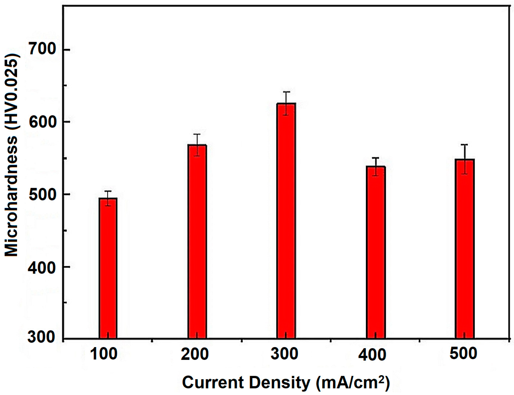
The deposit microhardness of the Sn-plated Ni coatings is shown in Figure 6. The microhardness of the Sn-plated Ni coatings increased from 498 to 620 HV with varying current density from 100 and 200 mA/cm2.
An increased microhardness of the coatings was attributed to the gradual grain refinement of Sn with increased current density. In addition, the coating microhardness displayed a decrease beyond 300 mA/cm2. This can be explained since, at higher current densities, hydrogen gas evolution at the cathode is rapid. Severe bubbling was observed at higher plating current densities that enhance the porosity levels, and a drop in the overall hardness was observed [34,35]. Therefore, coating microhardness depended upon the coupled effect of the grain size as well as the presence of the pores in the microstructures. Similar observations have been reported in the past for Sn-plated Cu coatings from pulse current plating [17,36].

3.5. Wear and Friction Studies

3.5.1. Wear Tracks

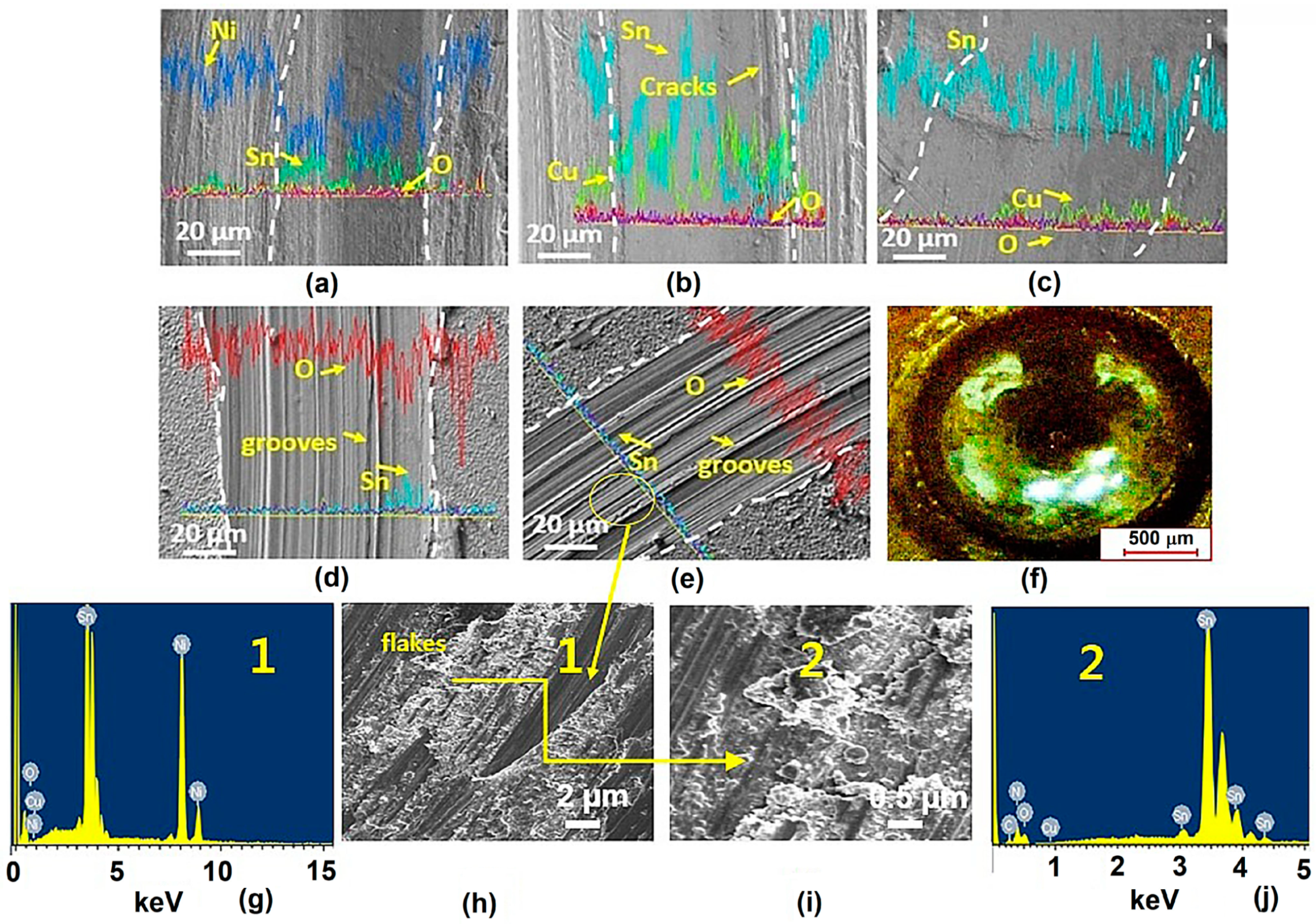
The worn-out surface morphology of the wear tracks after ball-on-disc wear is shown in Figure 7a–e. For wear track morphology, we selected the sample with the highest microhardness, plated at 300 mA/cm2. We can see that the width of the tracks was affected when the load was varied from 2 to 10 N. The line scan profile is also presented in the same SEM image for comparison. We found that at lower loading forces (2 N), the concentration of Ni and Sn was irregular across the track, being higher than Sn. It means the worn-out surface was non-uniform in Sn and Ni composition, with few scratches due to improper contact load. As the load increased to 4–6 N (Figure 7b,c), the wear surface turned slightly smooth and flat due to the proper sliding of the ball on the coating. The concentration of Sn improved gradually all over the surface, showing uniform wear (Figure 7c).
Further increase in loads (8–10 N) caused a severe form of the fine grooves across the matrix, which showed the hardening of the wear track due to continuous cyclic deformation at higher loads (Figure 7d,e). The formation of grooves was due to the plowing action of the indenter ball, leading to the hardening of the coating layer and further tearing by the harder WC indenter [37,38]. Additionally, at higher loads, the concentration of oxygen was prominent, which showed oxidative wear operating in a higher load regime due to the continuous increase in the rubbing of the surface by the ball indenter at higher loads [39]. A rough surface of the ball indenter showed material transfer from coatings to ball surface. This was confirmed by the surface image, as shown in Figure 8f.

3.5.2. Wear Factor and COF

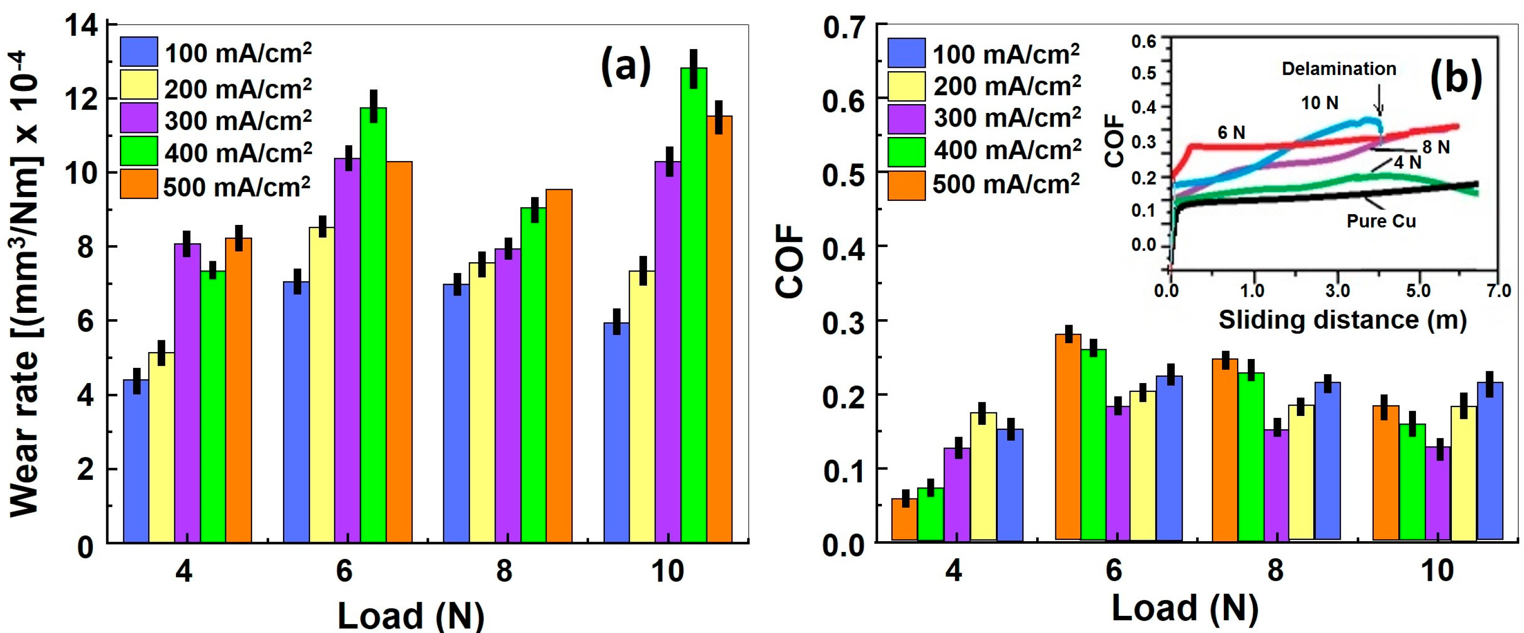
The wear factor and average COF experienced by the coatings at various loads are given in Figure 8a,b. The volume loss and wear factor of the coatings was minimum at 100 mA/cm2 in all cases. The wear factor of the coatings improved further at higher loads but did not change much until 6–8 N (at 200–300 mA/cm2). This was also because the microhardness of the films was highest at 300 mA/cm2. At higher loads and higher current density (10 N, 400–500 mA/cm2), the volume loss was severe, which led to a higher wear factor. The reason can be attributed to the lower microhardness and porous deposits plated at 400–500 mA/cm2, which failed at higher loads and higher current densities. Our results are consistent with those of wear resistance of AlCrSiN-coated tool steel [28].
Pure Cu foil had a constant COF of 0.14 at 10 N. If we compare the COF of the various coatings, we see that the COF was increasing continuously from 0.05 to 0.29 (Figure 8b). It can be due to the poor cathode coverage and globular rough deposits obtained at low current densities, where the coating was peeled off easily and the ball indenter scratched the wear tracks. The COF decreased a bit further at 200–300 mA/cm2 due to a higher thickness and uniform deposit density. The indenter ball smeared out uniformly, and COF was reduced. Under similar current densities, no significant change in COF was shown at higher loads. The COF decreased slightly and remained stable from 8–10 N which indicates that that ball indenter smoothened the surface and globular deposits or pores in the microstructure, leading to a reduction in COF. The COF was lowest at loads 6, 8, and 10 N for coatings plated at 300 mA/cm2. This may be attributed to the minimum surface roughness of coatings at 300 mA/cm2. A highly smooth surface will provide fewer obstructions to the ball in sliding. Such a type of slight variation in COF is attributed to the mixed adhesive and oxidative wear mechanism operating in the plated coatings. This was due to an increase in surface temperature due to the continuous rubbing of the tracks by the ball indenter with adherent secondary materials [40,41]. The steady-state value of the COF (≈0.3) at load 10 N was noticed due to the progressive smearing of the tracks, leading to a smooth contact at high sliding distances (Figure 8b, inset). The delamination seemed to occur before failure at around 4 m, as shown by the deviation in the COF curve (Figure 8b inset).

4. Summary and Conclusions

In this work, we successfully fabricated a Sn-plated Ni coating using a pulse plating technique from acidic electrolytes and investigated wear behavior using ball-on-disc wear tests. The coatings consisted of β-Sn and Ni with few minor IMCs, such as Ni3Sn and Cu20Sn6. Additionally, a small amount of metastable NiSn was also observed at lower current densities. An increase in the current density caused gradual refinement of grains up to 300 mA/cm2. However, a further rise in current density increased the deposit porosity due to the absorption of hydrogen bubbles in the coatings. The roughness was minimum while thickness was maximum at 300 mA/cm2. The coating microhardness was in a range from 498–620 HV, being maximum at 300 mA/cm2. The wear and friction behavior of the coatings revealed a volume loss increase with the normal loads applied. Under similar current density, the volume loss was higher at 10 N, while COF slightly decreased, showing oxidative wear at higher loads irrespective of the current density. The major wear mechanism of the Sn-plated Ni coatings may be proposed as a mixed adhesive and oxidation process at higher loads against the WC ball.

Author Contributions

Conceptualization and formal analysis, A.S. and B.A.; resources, B.A.; writing—original draft preparation, A.S.; writing—review and editing, A.S. and B.A.; funding acquisition, B.A. All authors have read and agreed to the published version of the manuscript.

Funding

This research was supported by the Basic Science Research Program through the National Research Foundation of Korea (NRF), funded by the Ministry of Education (Grant No. NRF-2018R1D1A1B07044481 (BA) and Grant No. NRF-2018R1D1A1B07044706 (AS)). This research was supported by the Nano·Material Technology Development Program through the National Research Foundation of Korea (NRF), funded by the Ministry of Science, ICT, and Future Planning (2009-0082580).

Data Availability Statement

The data presented in this study are available on request from the corresponding author. The data are not publicly available due to due to confidential nature of data.

Acknowledgments

This research was supported by the Basic Science Research Program through the National Research Foundation of Korea (NRF), funded by the Ministry of Education (Grant No. NRF-2018R1D1A1B07044481 (BA) and Grant No. NRF-2018R1D1A1B07044706 (AS)). This research was supported by the Nano·Material Technology Development Program through the National Research Foundation of Korea (NRF) funded by the Ministry of Science, ICT and Future Planning (2009-0082580).

Conflicts of Interest

The authors declare no conflict of interest.

References

  1. Osenbach, J.W.; DeLucca, J.M.; Potteiger, B.D.; Amin, A.; Baiocchi, F.A. Sn-whiskers: Truths and myths. In Lead-Free Electronic Solders; Springer: Boston, MA, USA, 2006. [Google Scholar]
  2. Sharma, A.; Das, S.; Das, K. Effect of different electrolytes on the microstructure, corrosion and whisker growth of pulse plated tin coatings. Microelectron. Eng. 2017, 170, 59–68. [Google Scholar] [CrossRef]
  3. Hektor, J.; Marijon, J.B.; Ristinmaa, M.; Hall, S.A.; Hallberg, H.; Iyengar, S.; Micha, J.S.; Robach, O.; Grennerat, F.; Castelnau, O. Evidence of 3D strain gradients associated with tin whisker growth. Scr. Mater. 2018, 144, 1–4. [Google Scholar] [CrossRef]
  4. Sharma, A.; Das, S.; Das, K. Pulse electrodeposition of lead-free tin-based composites for microelectronic packaging. In Electrodeposition of Composite Materials; Mohamed, A.M.A., Golden, T.D., Eds.; InTech: Rijeka, Croatia, 2016; pp. 253–274. [Google Scholar] [CrossRef] [Green Version]
  5. Sharma, A.; Das, S.; Das, K. Pulse electroplating of ultrafine grained tin coating. In Electroplating of Nanostructures; Mahmood, A., Ed.; Intech: Rijeka, Croatia, 2015; pp. 105–129. [Google Scholar] [CrossRef] [Green Version]
  6. Paunovic, M.; Schlesinger, M. Fundamentals of Electrochemical Deposition; Wiley Interscience: New York, NY, USA, 2006. [Google Scholar]
  7. Sharma, A.; Cheon, C.S.; Jung, J.P. Recent progress in electroless plating of copper. J. Microelectron. Packag. Soc. 2016, 23, 1–6. [Google Scholar] [CrossRef] [Green Version]
  8. Zhang, L.Z.; Bates, B.L.; Zhang, Y. Effect of post-deposition heat treatment on electrodeposited NiCoCrAlY coatings. Surf. Eng. 2017, 33, 136–141. [Google Scholar] [CrossRef]
  9. Jung, D.H.; Sharma, A.; Kim, K.H.; Choo, Y.C.; Jung, J.P. Effect of current density and plating time on Cu electroplating in TSV and low alpha solder bumping. J. Mater. Eng. Perform. 2015, 24, 1107–1115. [Google Scholar] [CrossRef]
  10. Sharma, A.; Bhattacharya, S.; Das, S.; Das, K. Fabrication of Sn–Ag/CeO2 electro-composite solder by pulse electrodeposition. Metall. Mater. Trans. A 2013, 44, 5587–5601. [Google Scholar] [CrossRef]
  11. Sharma, A.; Bhattacharya, S.; Das, S.; Das, K. Fabrication of Sn nanostructures by template assisted pulse electrodeposition. Surf. Eng. 2016, 32, 378–384. [Google Scholar] [CrossRef]
  12. Aniekwe, U.V.; Utigard, T.A. High-temperature oxidation of nickel-plated copper vs pure copper. Can. Metall. Q. 1999, 38, 277–281. [Google Scholar] [CrossRef]
  13. Harput, S. Fields of application of nickel plated copper conductor. In Sarkuysan Electrolytic Copper Document; Sarkuysan Electrolytic Copper Co.: Darıca, Turkey, 2006. [Google Scholar]
  14. Brusse, J.A.; Ewell, G.J.; Siplon, J.P. Tin Whiskers: Attributes and Mitigation. In Proceedings of the 22nd Capacitor and Resistor Technology Symposium, New Orleans, LA, USA, 25–29 March 2002; pp. 67–80. [Google Scholar]
  15. Wilson, G.C. The use of tin when alloyed with nickel or lead as a printed circuit finish. Trans. IMF 1972, 50, 109–113. [Google Scholar] [CrossRef]
  16. Jalota, S.K. Tin-nickel alloy plating. Met. Finish 2001, 99, 320–323. [Google Scholar] [CrossRef]
  17. Sharma, A.; Bhattacharya, S.; Das, S.; Das, K. A study on the effect of pulse electrodeposition parameters on the morphology of pure tin coatings. Metall. Mater. Trans. A 2014, 45, 4610–4622. [Google Scholar] [CrossRef]
  18. Sharma, A.; Bhattacharya, S.; Das, S.; Das, K. Influence of current density on surface morphology and properties of pulse plated tin films from citrate electrolyte. Appl. Surf. Sci. 2014, 290, 373–380. [Google Scholar] [CrossRef]
  19. Pewnim, N.; Roy, S. Electrodeposition of tin-rich Cu–Sn alloys from a methanesulfonic acid electrolyte. Electrochim. Acta 2013, 90, 498–506. [Google Scholar] [CrossRef]
  20. Sharma, A.; Bhattacharya, S.; Sen, R.; Reddy, B.S.B.; Fecht, H.J.; Das, K.; Das, S. Influence of current density on microstructure of pulse electrodeposited tin coatings. Mater. Charact. 2012, 68, 22–32. [Google Scholar] [CrossRef]
  21. Williamson, G.K.; Hall, W.H. X-ray line broadening from filed aluminum and wolfram. Acta Metall. 1953, 1, 22–31. [Google Scholar] [CrossRef]
  22. Ungar, T.; Dragomir, I.; Revesz, A.; Borbely, A. The contrast factors of dislocations in cubic crystals: The dislocation model of strain anisotropy in practice. J. Appl. Cryst. 1999, 32, 992–1002. [Google Scholar] [CrossRef] [Green Version]
  23. Rashidi, A.M.; Amadeh, A. The effect of current density on the grain size of electrodeposited nanocrystalline nickel coatings. Surf. Coat. Technol. 2008, 202, 3772–3776. [Google Scholar] [CrossRef]
  24. Standard Test Method for Linearly Reciprocating Ball-on-Flat Sliding Wear; ASTM G133–05; ASTM International: West Conshohocken, PA, USA, 2016.
  25. Bajwa, R.S.; Tudela, I.; Verbickas, R.; Palamarciuc, I.; Zhang, Y. Friction and wear performance of Sn-based coatings under hydrodynamic, mixed and boundary lubrication. Trib. Int. 2020, 149, 105695. [Google Scholar] [CrossRef]
  26. Ilangovan, S.; Sellamuthu, R. Effects of tin on hardness, wear rate and coefficient of friction of Cu–Ni–Sn alloys. J. Eng. Sci. Technol. 2013, 8, 34–43. [Google Scholar]
  27. Podgursky, V.; Gregor, A.; Adoberg, E.; Kulu, P. Wear of hard coatings, evaluated by means of KaloMax. Proc. Est. Acad. Sci. Eng. 2006, 12, 419–426. [Google Scholar]
  28. Drozd, K.; Walczak, M.; Szala, M.; Gancarczyk, K. Tribological behavior of AlCrSiN-coated tool steel K340 versus popular tool steel grades. Materials 2020, 13, 4895. [Google Scholar] [CrossRef] [PubMed]
  29. Szala, M.; Łatka, L.; Walczak, M.; Winnicki, M. Comparative study on the cavitation erosion and sliding wear of cold-sprayed Al/Al2O3 and Cu/Al2O3 coatings, and stainless steel, aluminium alloy, copper and brass. Metals 2020, 10, 856. [Google Scholar] [CrossRef]
  30. Zhu, J.; Ma, L.; Dwyer-Joyce, R.S. Friction and wear of Cu-15 wt.%Ni-8 wt.%Sn bronze lubricated by grease at room and elevated temperature. Wear 2020, 460–461, 203474. [Google Scholar] [CrossRef]
  31. Rosoiu, S.P.; Pantazi, A.G.; Petica, A.; Cojocaru, A.; Costovici, S.; Zanella, C.; Visan, T.; Anicai, L.; Enachescu, M. Comparative study of Ni–Sn alloys electrodeposited from choline chloride-based ionic liquids in direct and pulsed current. Coatings 2019, 9, 801. [Google Scholar] [CrossRef] [Green Version]
  32. Rooksby, H. An X-ray study of tin-nickel electrodeposits. Trans. IMF 1950, 27, 153–169. [Google Scholar] [CrossRef]
  33. Weil, R.; Cook, H.C. Electron-microscopic observations of the structure of electroplated nickel. J. Electrochem. Soc. 1962, 109, 295–301. [Google Scholar] [CrossRef]
  34. Schmitz, E.P.S.; Quinaia, S.P.; Garcia, J.R.; de Andrade, C.K.; Lopes, M.C. Influence of commercial organic additives on the nickel electroplating. Int. J. Electrochem. Sci. 2016, 11, 983–997. [Google Scholar]
  35. Ghosh, S.K.; Grover, A.K.; Dey, G.K.; Totlani, M.K. Nanocrystalline Ni–Cu alloy plating by pulse electrolysis. Surf. Coat. Technol. 2000, 126, 48–63. [Google Scholar] [CrossRef]
  36. Sharma, A.; Jang, Y.J.; Jung, J.P. Effect of current density on morphology of electroplated tin. Surf. Eng. 2015, 31, 458–464. [Google Scholar] [CrossRef]
  37. Matsui, I.; Takigawa, Y.; Yokoe, D.; Kato, T.; Uesugi, T.; Higashi, K. Strategy for electrodeposition of highly ductile bulk nanocrystalline metals with a face-centered cubic structure. Mater. Trans. 2014, 55, 1859–1866. [Google Scholar] [CrossRef] [Green Version]
  38. Sajjadnejad, M.; Omidvar, H.; Javanbakht, M.; Mozafari, A. Characterization of pure nickel coatings fabricated under pulse current conditions. Int. J. Mater. Metall. Eng. 2015, 9, 1061–1065. [Google Scholar]
  39. Bhattacharya, S.; Sharma, A.; Das, S.; Das, K. Synthesis and properties of pulse electrodeposited lead-free tin-based Sn/ZrSiO4 nanocomposite coatings. Metall. Mater. Trans. A 2016, 47, 1292–1312. [Google Scholar] [CrossRef]
  40. Mangam, V.; Bhattacharya, S.; Das, K.; Das, S. Friction and wear behavior of Cu–CeO2 nanocomposite coatings synthesized by pulsed electrodeposition. Surf. Coat. Technol. 2010, 205, 801–805. [Google Scholar] [CrossRef]
  41. Lee, K.U.; Jeong, D.K.; Joo, H.G.; Park, Y.W. Simulation for fretting corrosion of tin-coated copper contacts. Mater. Corr. 2011, 62, 352–356. [Google Scholar] [CrossRef]
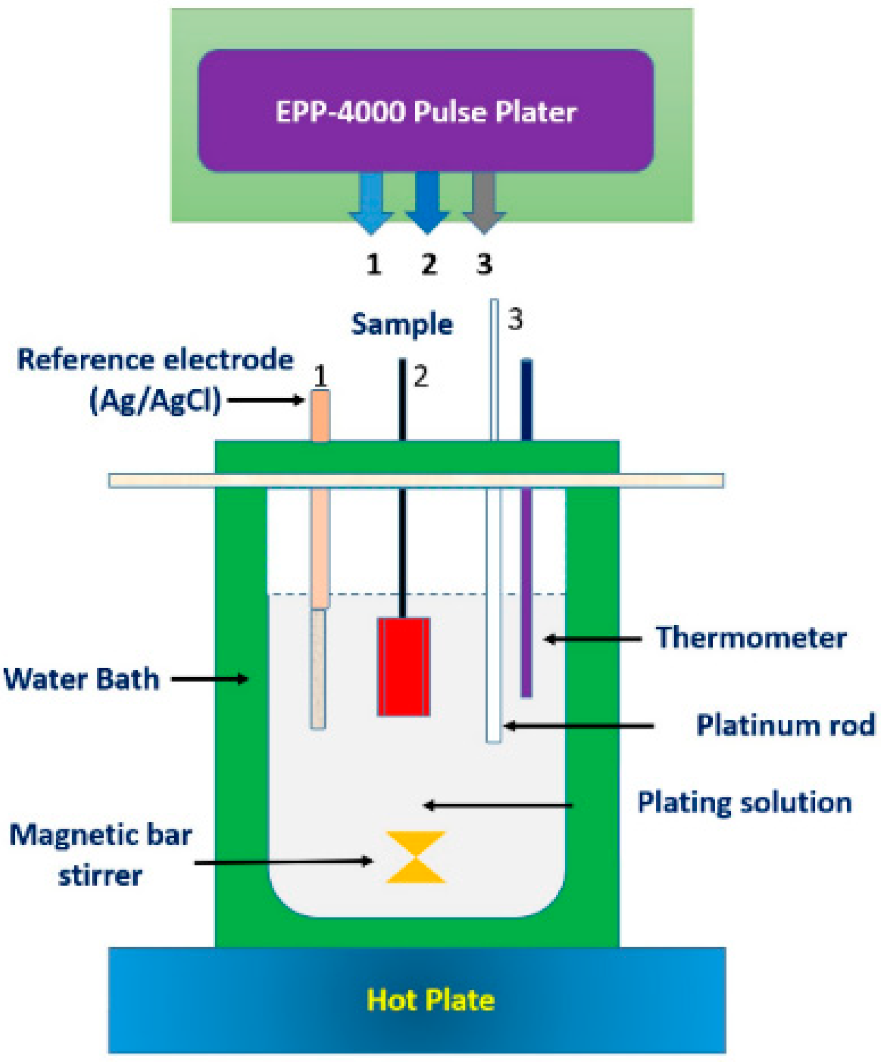
Figure 1. Experimental arrangement showing plating cell, electrodes, and power supply. The numbers 1, 2, and 3 indicate the connections to the EPP-4000 instrument.
Coatings 11 00056 g001
Figure 2. Ball-on-disc geometry of the wear test machine. The disc is rotating along the vertical axis with rotation speed ω.
Coatings 11 00056 g002
Figure 3. XRD pattern of Ni–Sn coatings plated at various current densities.
Coatings 11 00056 g003
Figure 4. Surface morphology of Sn-plated Ni at different current densities: (a) 100, (b) 200, (c) 300, (d) 400, and (e) 500 mA/cm2. The EDS spectrum of (c) is shown in (f). The inset shows the corresponding cross-section images. The black circles in (d,e) represent the pores in the coatings.
Coatings 11 00056 g004
Figure 5. (a) Deposit roughness and (b) thickness of the coatings at various current densities.
Coatings 11 00056 g005
Figure 6. Microhardness of the coatings at various current densities.
Coatings 11 00056 g006
Figure 7. SEM morphology of wear tracks after 7 m sliding at various normal loads: (a) 2, (b) 4, (c) 6, (d) 8, and (e) 10 N. The corresponding line scans were observed across the wear tracks. The plated current density was 300 mA/cm2. The surface image of the ball indenter after wear is shown in (f). The image of the ball indenter was shown when the ball was used at a load of 10 N and the sample plated at 300 mA/cm2. (gj) show the wear track EDS analysis of (e) at high resolution.
Coatings 11 00056 g007
Figure 8. Variation of (a) mean wear factor, and (b) mean coefficient of friction (COF) at different loads as a function of current density and normal loads. The inset shows the COF vs. sliding load distance.
Coatings 11 00056 g008
Table 1. Chemical bath compositions and operating parameters.
Composition of BathQuantity (g·L−1)Composition of BathQuantity (g·L−1)Operating ParametersValues
Ni PlatingSn Plating
NiSO4·6H2O300SnSO4150Current DensityNi: 300 mA/cm2
Sn: 100–500 mA/cm2
NiCl2·6H2O45 H2SO460On-time, Off-time0.001 s, 0.011 s
H3BO340 Triton X-1000.2Pulse Frequency100 Hz
Saccharin Sodium0.5 Duty Cycle9%
Sodium Dodecyl Sulfate0.1 Magnetic Stirring300 rpm
SubstrateCopper (cold rolled), 2 mm thick, Ra: 1 µm, Microhardness: 130 ± 8 HV
Table 2. Conditions for wear testing.
Normal Load (N)2–10 N
Sliding Distance (m)7
Linear Velocity (mm/s)3.8
Sliding Radius (mm)6
LubricantDry
Temperature (°C)30 °C
EnvironmentDry air
Ball IndenterWC (Tungsten Carbide), 2.0 mm, Grade G25
Specimen ShapeSn-plated Ni/Cu (30–55 µm Sn plated on
30 µm Ni over 25 × 25 × 2 mm3 Cu substrate)
Ball Indenter Hardness (HV)1750
Table 3. Compositional analysis of Sn-plated Ni/Cu coatings.
Current Density (mA/cm2)Composition (wt.%)
100Cu: 1.1, Ni: 7.10, Sn: 91.8
200Cu: 0.08, Ni: 9.56, Sn: 90.36
300Cu: 0.05, Ni: 14.68, Sn: 85.27
400Cu: 0.09, Ni: 25.36, Sn: 74.55
500Cu: 1.1, Ni: 34.67, Sn: 64.23
Publisher’s Note: MDPI stays neutral with regard to jurisdictional claims in published maps and institutional affiliations.