Abstract
Non-classical crystallization suggests that crystals can grow with nanoparticles as a building block. In this case, the crystallization behavior depends on the size and charge of the nanoparticles. If charged nanoparticles (CNPs) are small enough, they become liquid-like and tend to undergo epitaxial recrystallization. Here, the size effect of SiC CNPs on film crystallinity was studied in the hot-wire chemical vapor deposition process. To do this, SiC nanoparticles were captured under different processing conditions—in this case, wire temperature, precursor concentration and the filament bias. Increasing the temperature of tungsten wires and decreasing the ratio of (SiH4 + CH4)/H2 reduced the size of the SiC nanoparticles. When the nanoparticles were small enough, an epitaxial SiC film approximately 100-nm-thick was grown, whereas larger nanoparticles produced polycrystalline SiC films. These results suggest that the size of the CNPs is an important process variable when growing films by means of non-classical crystallization.
1. Introduction
Recently, a new mechanism of crystal growth has been proposed, in which crystals grow by nanosized-building blocks instead of growing by atoms, molecules or ions [1,2,3,4,5]. This new mechanism—referred to as non-classical crystallization—can explain many puzzling phenomena that could not be explained by conventional theories of classical crystallization. For example, a diamond film grows on a silicon substrate, whereas a porous skeletal soot structure grows on an iron substrate under identical conditions in the diamond chemical vapor deposition (CVD) process using hot wires or plasma [6,7,8].
This new mechanism is called the ‘theory of charged nanoparticles’ (TCN) [9]. According to this theory, the deposition behavior of nanoparticles changes drastically, depending on whether the nanoparticles are charged or neutral. Neutral nanoparticles tend to agglomerate randomly, producing a porous skeletal structure such as soot, whereas charged nanoparticles (CNPs) tend to be deposited as dense films or nanostructures instead of undergoing random Brownian coagulation. In order to explain the deposition of dense films or nanostructures without voids as well as epitaxial film growth via the building block of CNPs, Hwang [10] suggested that the presence of a charge should make the nanoparticles liquid-like, especially when they are small enough.
It has been confirmed experimentally that the size of the nanoparticles affects the deposition behavior of thin films and nanostructures. Jeon et al. [11] showed that the size of carbon CNPs increases with an increase in the concentration of CH4 during diamond CVD when using hot-wire CVD (HWCVD). They also showed that diamonds of a good quality level could be deposited with 1% CH4–99% H2 and that ball-like diamonds called cauliflower structures could be deposited with 3% CH4–99% H2. Jung et al. [12] could grew epitaxial Si thin films by continuously supplying relatively small nanoparticles while controlling the size of the nanoparticles using a shutter during the Si HWCVD process.
Recently, intensive efforts have been made to develop new semiconductor materials to replace Si, and SiC has attracted great attention as an alternative due to its promising physical properties [13,14,15,16,17,18,19,20,21]. Accordingly, an increasing number of studies have described attempts to grow SiC films of various structures by CVD [22,23,24]. Among the CVD methods, HWCVD has the advantages of offering deposition at a relatively low substrate temperature using wires at a high temperature, simple large-area deposition and a low equipment cost [25,26,27]. A few studies of the epitaxial growth of SiC using HWCVD have been conducted, though these have been limited to the studies of 3C–SiC on Si wafers [28,29,30,31]. Quite recently, 4H–SiC epitaxial deposition by means of HWCVD at a substrate temperature of 1500 °C was reported by Van Zeghbroeck et al. [32]. Kim et al. [33] confirmed that SiC nanoparticles were generated in the gas phase during the HWCVD process.
In this work, the size effect of SiC CNPs on the film crystallinity in the HWCVD process was studied. To do this, the wire temperature, the (SiH4 + CH4)/H2 ratio, and the filament bias were varied. An epitaxial 4H–SiC film layer with a thickness of approximately 100 nm could be grown when the wire temperature was 2300 °C, the (SiH4 + CH4)/H2 ratio was 0.01, bias of −50 V was applied to the wires, and the distance between the wires and the substrate was 2 mm.
2. Experimental Procedure
SiC nanoparticles and films were deposited using a HWCVD reactor, as shown in Figure 1. Three tungsten wires were resistively heated by a direct current (DC) power supply and the temperature of the wires was measured using an optical pyrometer. The temperature of tungsten wires was set to be between 1800 °C and 2300 °C. The distance between the wires and the substrate was 20 mm during the experiment, which captured SiC CNPs on a SiO membrane of a Cu-mesh grid. The distance was 2 or 8 mm in the experiment during the deposition of the SiC films. The temperature of a substrate was estimated to be 1500 °C and 1200 °C, respectively, at distances of 2 and 8 mm between the filaments and the substrate. The substrate temperature was estimated by computational fluid dynamics (CFD) calculations (Ansys fluent 17.0) with the boundary condition of the wire temperature measured by a two-color pyrometer. The substrates used for the deposition of the films were n-type, Si-face, 4H–SiC substrates off-angled by 4° toward the [110] direction. The pressure was 1 Torr.
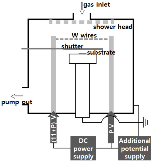
Figure 1.
Schematic of the hot-wire chemical vapor deposition (HWCVD) system showing the electric connections of the hot-wire DC power supply and the additional potential supply to apply bias to the wires.
Before the precursor gases were supplied, tungsten wires were treated under flowing hydrogen (H2, 99.9999%) at 1400 °C for ten minutes and carburized with methane (CH4, 99.9999%) at 2000 °C for 15 min. After changing the wire temperature to the deposition temperature, the deposition process was started with the addition of silane (SiH4, 99.9999%). The flow rate of H2 was fixed at 100 sccm. The ratio of CH4/SiH4 was 1. To study the effect of the precursor concentration on the size of the SiC CNPs, the ratio of (SiH4 + CH4)/H2 was varied, with ratios of 0.04, 0.02 and 0.01 used here. Deposition was prevented during the hydrogen treatment or during carbonization, as mentioned above, using a shutter, and the processing times were 30 s to capture SiC nanoparticles and 30 min to deposit the SiC films.
For resistive heating of the wires, a DC power supply was connected to both sides of the wires. The voltage was 11 V at the wire temperature of 2300 °C. To confirm the effect of the electric bias applied to the hot wires, an additional potential supply was installed in the HWCVD reactor, as shown in Figure 1. This additional potential supply for the bias forms a connection between the ground and the wire DC power supply. When the bias voltage is P, the potential difference between the ends of the wire is (11 + P) V at 2300 °C. The additional bias could be varied from −50 to +50 V.
The nanoparticles and the films were observed by HRTEM to confirm the size and crystallinity. HRTEM observations were carried out using a JEM-2100F device (JEOL, Ltd., Akisima, Japan) and a Tecnai F20 device (FEI Company, Hilsboro, OR, USA) with an accelerated voltage of 200 kV. Raman spectroscopy was performed using a LabRAM HR Evolution device (Horiba, Ltd., Kyoto, Japan) with a laser excitation wavelength of 532 nm to analyze the crystallinity of the films.
3. Results and Discussion
Figure 2 shows the TEM observation results of SiC nanoparticles captured on the SiO membrane of the Cu TEM grid at four different wire temperatures. When the wire temperature was 2300 °C, SiC nanoparticles 2–3 nm in size were captured, while those 5–8 nm in size were captured at 2000 °C. This shows that the size of the SiC nanoparticles increases with a decrease in the wire temperature. In contrast, the number concentration of the nanoparticles was not greatly affected by the temperature. On the other hand, when the temperature was lowered to 1800 °C, much larger Si nanoparticles instead of SiC nanoparticles were deposited. This occurred because the temperature of the tungsten wire was not high enough to decompose all of the CH4 supplied by the shower head. It should be noted that CH4 is much more difficult to decompose than SiH4.
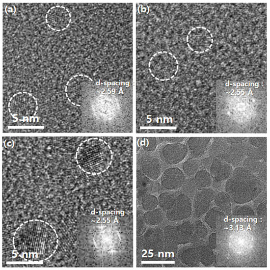
Figure 2.
TEM images of SiC nanoparticles on a SiO membrane of a TEM grid at wire temperatures of (a) 2300 °C, (b) 2200 °C, (c) 2000 °C and (d) 1800 °C.
During the HWCVD process, hot wires play an important role, not only in decomposing precursor gases but also in charging nanoparticles by means of thermionic electron emission. Based on TCN, if CNPs are small enough at the given temperature, they tend to have a liquid-like property and to undergo epitaxial recrystallization, processes capable of producing epitaxial films. If CNPs are not small enough, epitaxial recrystallization does not proceed well, leading to twin or grain boundaries on the growing surface. Nonetheless, CNPs produce a void-free dense structure of films.
Increasing the deposition temperature is another way to make CNPs liquid-like. If CNPs are liquid-like, they can accommodate their structure to that of the substrate, which is beneficial for epitaxial growth [10,12,34]. Therefore, increasing the wire temperature would be favorable for epitaxial growth. When the wire temperature exceeds 2300 °C, however, tungsten tends to evaporate from the wires, contaminating the films. Therefore, during the HWCVD process using tungsten wires, the wire temperature should not exceed 2300 °C [35].
Figure 3a–c show TEM images of captured SiC nanoparticles with varying ratios of (SiH4 + CH4)/H2 of 0.04, 0.02 and 0.01, respectively. Under all three conditions, SiC nanoparticles 1–3 nm in size were captured. Regarding the size of the nanoparticles, there appears to be little difference with different precursor concentrations. On the other hand, as the precursor concentration decreased, the number concentration of SiC nanoparticles also decreased. When the gas ratio of (SiH4 + CH4)/H2 was 0.01, only a few nanoparticles 1–2 nm in size were observed.
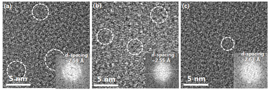
Figure 3.
TEM images of SiC nanoparticles captured with the gas ratios of (SiH4 + CH4)/H2 of (a) 0.04, (b) 0.02 and (c) 0.01.
Figure 4 shows the capturing behavior of SiC nanoparticles on the SiO membrane when electric bias was applied to the hot wires using the additional power supply, as shown in Figure 1. When bias of +50 V was applied to the hot wires, the size and number concentration of the SiC nanoparticles were similar to those at 0 V, as shown in Figure 4a,b.
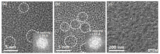
Figure 4.
TEM and STEM images of SiC nanoparticles with additional hot-wire biases of (a) 0 V, (b) +50 V and (c) −50 V.
In contrast, no SiC nanoparticles were observed when −50 V was applied to the hot wires. However, with regard to this result, the lack of the observation of SiC nanoparticles does not mean that they are absent. When the size of the CNPs is small enough, they can accommodate their structure to that of the amorphous SiO membrane. In such a case, they cannot be observed. If this explanation is correct, the SiC film grown on the SiC wafer would have a high epitaxial quality level under the condition of −50 V. This is discussed in Figure 5.
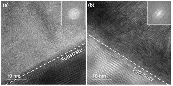
Figure 5.
TEM cross-section and fast Fourier transform (FFT) images of SiC films deposited at (SiH4 + CH4)/H2 gas ratios of (a) 0.04 and (b) 0.01.
Park et al. [36] studied the electric field which forms around the hot wires during Si HWCVD using software from Maxwell. They also measured the current near the input and output positions of the hot wires when the DC bias was applied to the hot wires. When bias was +25 V, the measured current was +2.38 nA cm−2 at a position 1.5 cm below the hot wires input position. When bias of −25 V was applied to the hot wires, however, the result was −4.86 × 10⁴ nA cm−2 at the same position. This means that when negative bias is applied to the hot wires, a much higher density of electrons or negatively charged species can be produced. High-density negatively charged nanoparticles electrically repel each other, leading to smaller CNPs.
Fujita [37,38] reported that if nanoparticles are below a certain size, referred to as the “magic size,” their properties, specifically the diffusivity, changes abruptly. For example, the diffusivity increases abruptly and reaches a high level below the magic size so that small nanoparticles nearly reach a liquid-like state. Fujita suggested that the magic size for SiC is in the range of 3–5 nm. If Fujita’s concept of the magic size is combined with the theory of CNPs, small CNPs tend to be liquid-like and to accommodate their structure to that of the substrate. Considering such an abruptly high diffusivity below the magic size, the smallest CNPs would be favorable for epitaxial recrystallization under the given temperature. The smallest CNPs can be expected when the gas ratio of (SiH4 + CH4)/H2 is 0.01 and bias of −50 V is applied to the hot wires at the same time. In other words, in this condition, the size of CNPs would be so small that liquid-like CNPs form and accommodate their structure to that of the SiO membrane.
Figure 5 shows a cross-section TEM image of SiC films deposited at (SiH4 + CH4)/H2 gas ratios of 0.04 and 0.01 under a bias condition of −50 V at wire temperature of 2300 °C. The TEM and the fast Fourier transform (FFT) images shown in Figure 5a after deposition at the gas ratio of (SiH4 + CH4)/H2 of 0.04, shows that a polycrystalline SiC film was grown. However, those in Figure 5b, with deposition taking place at the (SiH4 + CH4)/H2 gas ratio of 0.01, show that an epitaxial 4H–SiC film of approximately 30 nm was grown.
Figure 5 is in good agreement with the hypothesis stemming from the theory of CNPs: small CNPs are liquid-like and favorable for epitaxial growth, whereas large CNPs are less liquid-like and favorable for poly-structure growth. According to the theory of CNPs, if the substrate temperature is increased, it would be favorable for epitaxial growth even further. To increase the substrate temperature, the distance between the hot wires and the substrate was reduced from eight millimeters to two millimeters with the other conditions identical to those in Figure 5b. This result is shown in Figure 6, where an epitaxial 4H–SiC film of approximately 100 nm was grown.
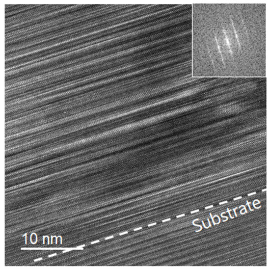
Figure 6.
TEM cross-section and FFT images of a SiC film deposited at a (SiH4 + CH4)/H2 gas ratio of 0.01, wire bias of −50 V and distance of 2 mm between the wires and the substrate.
In our previous study, the size of SiC nanoparticles increased with increasing process time [33]. When additional bias of −50 V was applied to the hot wires at a gas ratio of (SiH4 + CH4)/H2 of 0.01, the initial size of the nanoparticles was small enough to accommodate their structure to the structure of the substrates. As the size of nanoparticles increases with process time, larger nanoparticles deposited as a building block of films. According to the TCN, large nanoparticles do not change their structure to the substrate. Therefore, polycrystalline SiC films were deposited on the initial growth of the epitaxial films.
Figure 7 shows the Raman spectra of SiC films deposited under various conditions. Figure 7a–c show the data when the gas ratio of (SiH4 + CH4)/H2 was 0.04 and the distance between the wires and the substrate was 8 mm, respectively, without bias, with bias of +50 V and with bias of –50 V applied to the wires. In Figure 7a,b amorphous SiC (a–SiC) peaks were observed in the region with a low Raman shift. Silicon peaks were also observed at 520 cm−1.
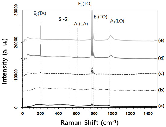
Figure 7.
Raman spectra of the SiC films deposited under five different conditions: (a) without bias and at a gas ratio of (SiH4 + CH4)/H2 of 0.04, (b) with bias of +50 V and at a gas ratio of (SiH4 + CH4)/H2 of 0.04, (c) with bias of −50 V and at a gas ratio of (SiH4 + CH4)/H2 of 0.04, (d) with bias of −50 V and at a gas ratio of (SiH4 + CH4)/H2 of 0.01 and (e) with bias of −50 V, a gas ratio of (SiH4 + CH4)/H2 of 0.01 and a distance of 2 mm between the wires and the substrate.
Figure 7d shows the Raman spectrum of the SiC film with bias of −50 V applied to the wires and the distance between the wires and the substrate being 8mm when the gas ratio of (SiH4 + CH4)/H2 was 0.01. In Figure 7c,d, the higher intensity of the 4H–SiC transverse optical (TO) at a Raman shift of 776 cm−1 corresponds to the higher crystallinity. Figure 7e shows the Raman spectrum of the SiC film with bias of −50 V at the gas ratio of 0.01 when the distance between the wires and the substrate decreased to 2 mm. The peak intensities for 4H–SiC TO at 776 cm−1 in Figure 7d,e are much higher than those in Figure 7a–c. According to a comparison of the peak intensity between Figure 7d,e—reducing the distance between the wires and the substrate from 8 mm to 2 mm increases the crystalline quality.
4. Conclusions
In this study, we investigated the effect of the size of charged nanoparticles on the crystallinity of SiC films in the HWCVD process based on non-classical crystallization. The size of the captured SiC nanoparticles decreased with an increase in the wire temperature to 2300 °C, a decrease in the precursor gas ratio of (SiH4 + CH4)/H2 from 0.04 to 0.01 and applying negative bias to the hot wires.
It was confirmed that the crystallinity of films was improved by the Raman spectra when small charged nanoparticles were generated in the gas phase by such as negative wire bias and low precursor concentration. An epitaxial film of approximately 30 nm was obtained when small SiC nanoparticles were used. This was achieved by decreasing the precursor concentration and applying negative bias to the wires. Raising the substrate temperature by reducing the distance between the wires and the substrate from eight millimeters to two millimeters made it possible to grow epitaxial 4H–SiC film to a thickness of approximately 100 nm. Based on these results, it is suggested that the size of CNPs and the temperature of substrates are important factors of the crystallinity of films.
Author Contributions
Conceptualization, D.K.; methodology, D.K., D.-Y.K. and J.-H.K.; formal analysis, D.K., D.-Y.K. and J.-H.K.; investigation, D.K., D.-Y.K. and J.-H.K.; data curation, D.K., D.-Y.K. and J.-H.K.; writing—original draft preparation, D.K.; writing—review and editing, D.K. and N.-M.H.; supervision, N.-M.H. All authors have read and agreed to the published version of the manuscript.
Funding
This work was supported by the National Research Foundation of Korea (NRF) grant funded by the Korea government (MSIT) (No. 2020R1A5A6017701) and by Global Frontier Program through the Global Frontier Hybrid Interface Materials (GFHIM) of the National Research Foundation of Korea (NRF) funded by the Ministry of Science, ICT and Future Planning (MSIP) (No. 2013M3A6B1078874).
Conflicts of Interest
The authors declare no conflict of interest.
References
- Cölfen, H.; Markus, A. Mesocrystals and Nonclassical Crystallization; Wiley: Hoboken, NJ, USA, 2008. [Google Scholar]
- Zhang, Q.; Liu, S.-J.; Yu, S.-H. Recent advances in oriented attachment growth and synthesis of functional materials: Concept, evidence, mechanism, and future. J. Mater. Chem. 2009, 19, 191–207. [Google Scholar] [CrossRef]
- Garscadden, A.; Ganguly, B.N.; Haaland, P.D.; Williams, J. Overview of growth and behaviour of clusters and particles in plasmas. Plasma Sources Sci. Technol. 1994, 3, 239–245. [Google Scholar] [CrossRef]
- Stoffels, E.; Stoffels, W.W.; Kroesen, G.M.W.; De Hoog, F.J. Dust formation and charging in an Ar/SiH4 radio-frequency discharge. J. Vac. Sci. Technol. A 1996, 14, 556–561. [Google Scholar] [CrossRef]
- Gebauer, D.; Cölfen, H. Prenucleation clusters and non-classical nucleation. Nano Today 2011, 6, 564–584. [Google Scholar] [CrossRef]
- Hwang, N.-M.; Hahn, J.; Yoon, D. Charged cluster model in the low pressure synthesis of diamond. J. Cryst. Growth 1996, 162, 55–68. [Google Scholar] [CrossRef]
- Huh, J.-M.; Yoon, D.-Y.; Kim, D.-Y.; Hwang, N.-M. Effect of substrate materials in the low-pressure synthesis of diamond: Approach by theory of charged clusters. Z. Metallkd. 2005, 96, 225–232. [Google Scholar] [CrossRef]
- Weiser, P.S.; Prawer, S.; Hoffman, A.; Manory, R.R.; Paterson PJ, K.; Stuart, S.A. Carbon diffusion in uncoated and titanium nitride coated iron substrates during microwave plasma assisted chemical vapor deposition of diamond. J. Appl. Phys. 1992, 72, 4643–4647. [Google Scholar] [CrossRef]
- Hwang, N.-M.; Lee, D.-K. Charged nanoparticles in thin film and nanostructure growth by chemical vapour deposition. J. Phys. D Appl. Phys. 2010, 43, 3001–3038. [Google Scholar] [CrossRef]
- Hwang, N.-M. Non-Classical Crystallization of Thin Films and Nanostructures in CVD and PVD Processes; Springer: Dordrecht, The Netherlands, 2016. [Google Scholar]
- Jeon, I.-D.; Park, C.-J.; Kim, D.-Y.; Hwang, N.-M. Effect of methane concentration on size of charged clusters in the hot filament diamond CVD process. J. Cryst. Growth 2001, 223, 6–14. [Google Scholar] [CrossRef]
- Jung, J.-S.; Lee, S.-H.; Kim, D.-S.; Kim, K.-S.; Park, S.-W.; Hwang, N.-M. Non-classical crystallization of silicon thin films during hot wire chemical vapor deposition. J. Cryst. Growth 2017, 458, 8–15. [Google Scholar] [CrossRef]
- Jones, E.A.; Wang, F.F.; Costinett, D. Review of commercial GaN power devices and GaN-based converter design challenges. IEEE J. Emerg. Sel. Top. Power Electron. 2016, 4, 707–719. [Google Scholar] [CrossRef]
- Chow, T.P. Wide bandgap semiconductor power devices for energy efficient systems. In Proceedings of the 2015 IEEE 3rd Workshop on Wide Bandgap Power Devices and Applications, Blacksburg, VA, USA, 2–4 November 2015; pp. 402–405. [Google Scholar]
- Chow, T.P. Progress in high voltage SiC and GaN power switching devices. In Silicon Carbide and Related Materials 2013: Selected, Proceedings of the 15th International Conference on Silicon Carbide and Related Materials (ICSCRM 2013), Miyazaki, Japan, 29 September–4 October 2013; Hajime, O., Hiroshi, H., Tsunenobu, K., Masahiro, Y., Heiji, W., Tomoaki, H., Hideharu, M., Tsuyoshi, F., Yasuhisa, S., Eds.; Trans Tech Publications, Ltd.: Stafa-Zurich, Switzerland, 2014; pp. 1077–1082. [Google Scholar]
- Millán, J.; Godignon, P.; Perpiñà, X.; Pérez-Tomás, A.; Rebollo, J. A survey of wide bandgap power semiconductor devices. IEEE Trans. Power Electron. 2013, 29, 2155–2163. [Google Scholar] [CrossRef]
- Burgener, R.H., II; Felix, R.L.; Renlund, G.M. Group II-VI Semiconductor Devices. U.S. Patent 7227196B2, 5 June 2007. [Google Scholar]
- She, X.; Huang, A.Q.; Lucía, Ó.; Ozpineci, B. Review of silicon carbide power devices and their applications. IEEE Trans. Ind. Electron. 2017, 64, 8193–8205. [Google Scholar] [CrossRef]
- Guo, X.; Xun, Q.; Li, Z.; Du, S. Silicon carbide converters and MEMS devices for high-temperature power electronics: A critical review. Micromachines 2019, 10, 406. [Google Scholar] [CrossRef]
- Benemanskaya, G.; Dementev, P.; Kukushkin, S.; Osipov, A.; Timoshnev, S. Carbon-based aromatic-like nanostructures on the vicinal SiC surfaces induced by Ba adsorption. ECS J. Solid State Sci. Technol. 2019, 8, M53. [Google Scholar] [CrossRef]
- Chen, J.; Du, X.; Luo, Q.; Zhang, X.; Sun, P.; Zhou, L. A review of switching oscillations of wide bandgap semiconductor devices. IEEE Trans. Power Electron. 2020. [Google Scholar] [CrossRef]
- Tokuda, Y.; Makino, E.; Sugiyama, N.; Kamata, I.; Hoshino, N.; Kojima, J.; Hara, K.; Tsuchida, H. Stable and high-speed SiC bulk growth without dendrites by the HTCVD method. J. Cryst. Growth 2016, 448, 29–35. [Google Scholar] [CrossRef]
- Kim, S.; Suh, S.; Jeong, J.K.; Kim, H.J. Numerical study on the growth rate of silicon carbide single crystals in a high temperature chemical vapor deposition system. J. Nanosci. Nanotechnol. 2017, 17, 8344–8349. [Google Scholar] [CrossRef]
- Cheng, H.; Yang, M.; Lai, Y.; Hu, M.; Li, Q.; Tu, R.; Zhang, S.; Han, M.; Goto, T.; Zhang, L. Transparent highly oriented 3C-SiC bulks by halide laser CVD. J. Eur. Ceram. Soc. 2018, 38, 3057–3063. [Google Scholar] [CrossRef]
- Tarazona, A.; Bucio, T.D.; Oo, S.; Petra, R.; Khokhar, A.; Boden, S.A.; Gardes, F.; Reed, G.; Chong, H. Hot wire chemical vapor deposition for silicon photonics: An emerging industrial application opportunity. Thin Solid Films 2019, 676, 26–30. [Google Scholar] [CrossRef]
- Oo, S.; Tarazona, A.; Khokhar, A.; Petra, R.; Franz, Y.; Mashanovich, G.; Reed, G.; Peacock, A.; Chong, H. Hot-wire chemical vapour deposition low-loss a-Si: H waveguides for silicon photonic devices. Photonics Res. 2019, 7, 193–200. [Google Scholar] [CrossRef]
- Ramos, J.R.; Morales, C.; Matsumoto, Y. Oxygen concentration effect on properties of SiOC thin films obtained by HWCVD. In Proceedings of the 14th International Conference on Electrical Engineering, Computing Science and Automatic Control. (CCE), Mexico City, Mexico, 20–22 October 2017; pp. 1–4. [Google Scholar] [CrossRef]
- Zhiyong, Z.; Wu, Z.; Xuewen, W.; Tianming, L.; Zhiming, C.; Shuixian, Z. Epitaxial monocrystalline SiC films grown on Si by HFCVD at 780 °C. Mater. Sci. Eng. B 2000, 75, 177–179. [Google Scholar] [CrossRef]
- Wu, Z.; Zhang, Z.-Y.; Deng, Z.-H.; Wang, X.-W.; Yan, J.-F.; Ni, Y.-J. Epitaxial growth of SiC films at low temperature and its photoluminescence. In Proceedings of the 8th International Conference on Solid-State and Integrated Circuit Technology, Shanghai, China, 23–26 October 2006; pp. 932–934. [Google Scholar]
- Yasui, K.; Eto, J.; Narita, Y.; Takata, M.; Akahane, T. Low-temperature heteroepitaxial growth of SiC on (100) Si using hot-mesh chemical vapor deposition. Jpn. J. Appl. Phys. 2005, 44, 1361. [Google Scholar] [CrossRef]
- Hens, P.; Brow, R.; Robinson, H.; Cromar, M.; Van Zeghbroeck, B. Epitaxial growth of cubic silicon carbide on silicon using hot filament chemical vapor deposition. Thin Solid Films 2017, 635, 48–52. [Google Scholar] [CrossRef]
- Van Zeghbroeck, B.; Robinson, H.; Brow, R.R. Hot filament CVD growth of 4H-SiC epitaxial layers. In Proceedings of the International Conference on Silicon Carbide and Related Materials 2017, Washington, DC, USA, 17–22 September 2017; Trans Tech Publications, Ltd.: Zurich, Switzerland, 2018; pp. 120–130. [Google Scholar]
- Kim, D.; Kim, D.Y.; Kwon, J.H.; Kim, K.-S.; Hwang, N.-M. Generation of charged SiC nanoparticles during HWCVD process. Electron. Mater. Lett. 2020, 16, 1–8. [Google Scholar] [CrossRef]
- Lee, S.C.; Yu, B.D.; Kim, D.-Y.; Hwang, N.-M. Effects of cluster size and substrate temperature on the homoepitaxial deposition of Au clusters. J. Cryst. Growth 2002, 242, 463–470. [Google Scholar] [CrossRef]
- Menon, P.M.; Edwards, A.G.; Feigerle, C.S.; Shaw, R.W.; Coffey, D.W.; Heatherly, L.J.; Clausing, R.E.; Robinson, L.; Glasgow, D.C. Filament metal contamination and Raman spectra of hot filament chemical vapor deposited diamond films. Diam. Relat. Mater. 1999, 8, 101–109. [Google Scholar] [CrossRef]
- Park, S.Y.; Yang, S.M.; Kim, C.S.; Hwang, N.M. Effect of bias applied to hot wires on generation of positive and negative charges during silicon hot-wire chemical vapor deposition. J. Phys. Chem. C 2009, 113, 17011–17017. [Google Scholar] [CrossRef]
- Fujita, H. Atom clusters—New applications of high-voltage electron microscopy “micro-laboratory” to materials science. Ultramicroscopy 1991, 39, 369–381. [Google Scholar] [CrossRef]
- Fujita, H. The magic size and the magic number of atom clusters. Sci. Technol. 1995, 7, 9–20. [Google Scholar]
© 2020 by the authors. Licensee MDPI, Basel, Switzerland. This article is an open access article distributed under the terms and conditions of the Creative Commons Attribution (CC BY) license (http://creativecommons.org/licenses/by/4.0/).