Article

Investigation of Conductive Mechanism of Amorphous IGO Resistive Random-Access Memory with Different Top Electrode Metal

1
Institute of Microelectronics & Department of Electrical Engineering, National Cheng Kung University, Tainan 70101, Taiwan
2
Institute of Microelectronics & Department of Electrical Engineering, Department of Photonics, Advanced Optoelectronic Technology Center, National Cheng Kung University, Tainan 70101, Taiwan
*
Author to whom correspondence should be addressed.
Coatings 2020, 10(5), 504; https://doi.org/10.3390/coatings10050504
Submission received: 21 April 2020 / Revised: 15 May 2020 / Accepted: 21 May 2020 / Published: 24 May 2020
(This article belongs to the Special Issue Advances in Thin Film Transistors: Properties and Applications)

Abstract

:
In this paper, resistive random-access memory (RRAM) with InGaO (IGO) as an active layer was fabricated by radio-frequency (RF) sputtering system and the resistive switching mechanism with the different top electrode (TE) of Pt, Ti, and Al were investigated. The Pt/IGO/Pt/Ti RRAM exhibits typical bipolar resistive switching features with an average set voltage of 1.73 V, average reset voltage of −0.60 V, average high resistance state (HRS) of 54,954.09 Ω, and the average low resistance state (LRS) of 64.97 Ω, respectively. Ti and Al were substituted for Pt as TE, and the conductive mechanism was different from TE of Pt. When Ti and Al were deposited onto the switching layer, both TE of Ti and Al will form oxidation of TiOx and AlOx because of their high activity to oxygen. The oxidation will have different effects on the forming of filaments, which may further affect the RRAM performance. The details of different mechanisms caused by different TE will be discussed. In brief, IGO is an excellent candidate for the RRAM device and with the aids of TiOx, the set voltage, and reset voltage, HRS and LRS become much more stable.

1. Introduction

In recent years, metal-oxide semiconductor (MOS) transistor-based memories such as dynamic random-access memory (DRAM) and NAND flash memory play a critical role in the computer science industry. However, with the progress of science and technology, more and more demands which cannot be satisfied with those traditional memories are required. Nowadays, emerging non-volatile memories (NVMs) are, therefore, being widely researched and developed due to its fast operation speed and low power consumption [1,2,3,4,5,6,7,8,9,10]. Emerging NVMs can be simply divided into three categories as magnetic random-access memory (MRAM), phase change random-access memory (PCM), and resistive random-access memory (RRAM).
The MRAM structure based on memory cells that have two magnetic storage elements, one with a fixed magnetic polarity and the other with switchable polarity. Technically, the state of MRAM can be confirmed by conducting a current through the cell to determine the value of electrical resistance. According to the magnetic tunnel effect [11], the electrons will be able to tunnel to switch the cells from different states. On the other hand, PCM is based on a class of material called chalcogenide glasses which can exist in two different phase states (e.g., crystalline and amorphous) [12]. By applying a current, the crystal structure of the material can change rapidly between the two states which leads to different electrical resistances. Among all, owing to being faster than PCM and smaller than MRAM, RRAM is considered as the candidate with the most potential. Besides, the RRAM device has a simpler structure compared to others and is more compatible with CMOS technology.
Due to the simple sandwich-structure of the RRAM device—which consists of top electrode (TE), metal oxide, and bottom electrode (BE) —RRAM is easy to fabricate. A lot of oxide materials—such as HfO2 [13,14], ZrO2 [15,16], Al2O3 [17,18], TiO2 [19,20], NiO [21], SrZrO3 [22], HfZrO [23], IGZO [24], ZnO [25], etc.—were fabricated as the RRAM active layer and have been reported. As a wide bandgap material, Ga2O3-based oxide has also been commonly used for devices such as thin film transistor (TFT) [26,27], photodectector [28,29], high electron mobility transistor (HEMT) [30], and so on. However, research on Ga2O3-based RRAM is still in its infancy. Only J. B. Yang’s team has researched the RRAM performance using InGaO (IGO) as an active layer [31]. In this work, IGO was chosen to be the active layer because of its favorable electron mobility, ideal optical transparency, and low-temperature processability.
As everyone knows, RRAM devices were operated between high resistance state (HRS) and low resistance state (LRS). The resistance switching (RS) behavior was caused by the filament which was arrayed by the oxygen vacancies. That is to say, the oxygen vacancies may be arrayed under an electric field and the arrayed oxygen vacancies are what we called a filament. The filament can be formed by the set process and destroyed by the reset process. However, lots of reports have pointed out that different TE materials will have different influence on the arrangement of the oxygen vacancies at the interface between TE and active layer [32,33,34,35], for instance, the mechanism the filament be formed and be destroyed and the paths the filament may grow. The above uncertainties caused by different TEs may further affect the performance of the RRAM device. In order to analyze the mechanism of different TEs, the inert metal Pt is chosen to be the standard TE. Except for the inert metal Pt, we choose another two metals with a similar work function of about 4.3 eV, which is Ti (4.33 eV) and Al (4.28 eV) [36], to deeply research the influence of the RRAM device.
In this work, high-performance RRAM using IGO as an active layer was fabricated by RF sputtering system. The characteristics of the IGO thin film were reported. Besides, we focus on the mechanism of how different TE materials affect RRAM performance.

2. Experimental Details

Figure 1 shows the structure of the IGO RRAM. The proposed RRAM was fabricated on 2 cm × 2 cm quartz substrates which were cleaned with an ultrasonicator by acetone, isopropyl alcohol, and deionized water each for 5 min. After drying under a stream of nitrogen, 10-nm-thick Ti adhesion layer and 50-nm-thick Pt bottom electrode were evaporated onto the substrates by e-beam evaporator in order. 20-nm-thick IGO was then deposited by radio frequency (RF) sputtering system as an active layer using a single InGaO target (In2O3:Ga2O3 = 40:60 in at %). During the sputtering process, the sputtering power was set at 80 W, the background pressure was fixed at 5 mtorr, and the gas flow ratio of O2/Ar was 10/90 sccm, respectively. Finally, 50-nm-thick Pt, 100-nm-thick Ti, and 100-nm-thick Al were deposited each by e-beam as different TEs. On the other hand, the size of the RRAM device was patterned by metal masks, which was 1500 μm × 1500 μm for the active layer and 50 μm × 50 μm for the TE, respectively.
To verify the quality and characteristics of the deposited thin film, X-ray diffraction (XRD: Bruker D8 Discover, Billerica, MA, USA), atomic force microscope (AFM: Bruker, Billerica, MA, USA), and transmission electron microscope (TEM: JEM-2100F Electron Microscope, JEOL, Tokyo, Japan) analysis were carried out. In addition, the current–voltage (I–V) characteristics were measured at room temperature by Agilent B1500A semiconductor parameter analyser (Agilent, Santa Clara, CA, USA).

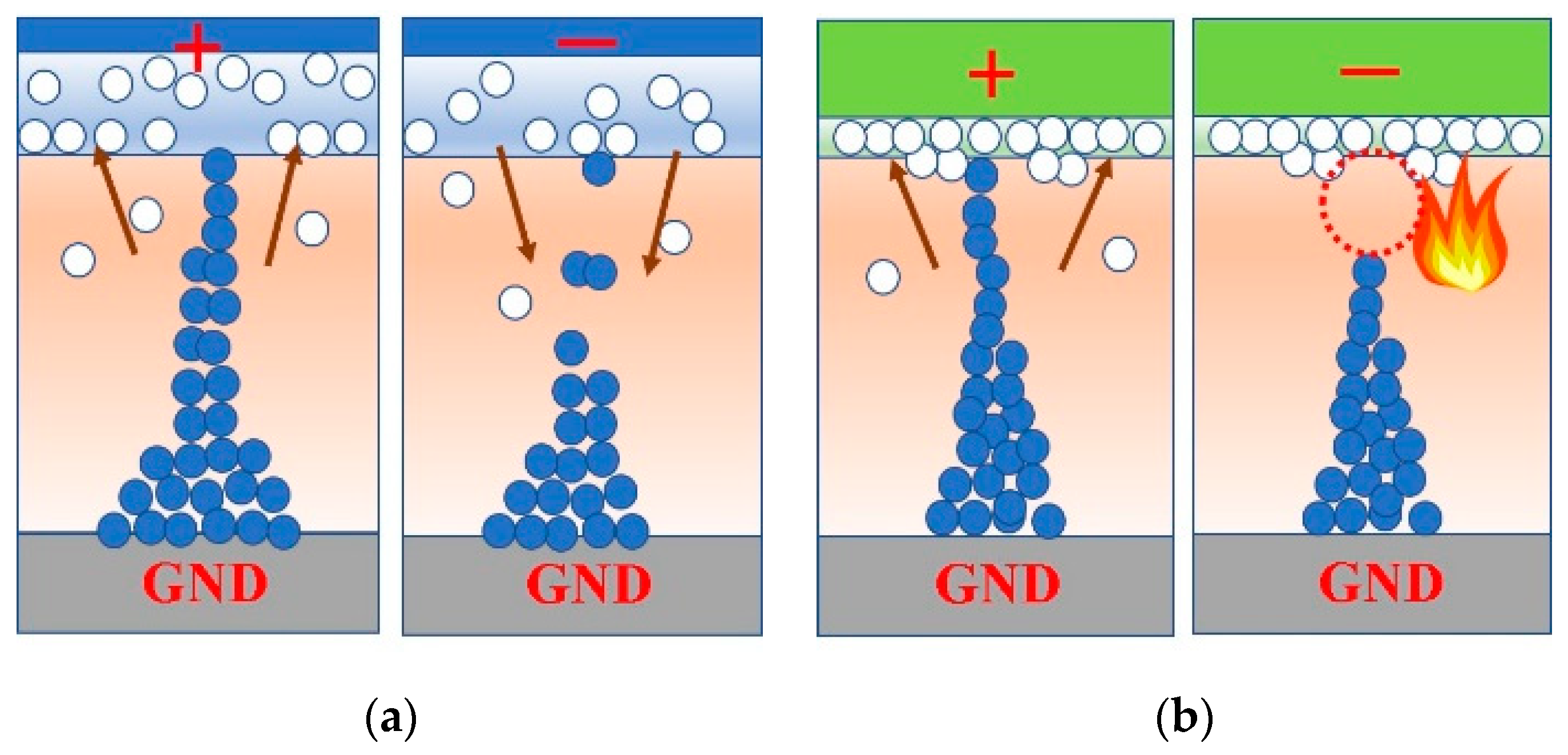
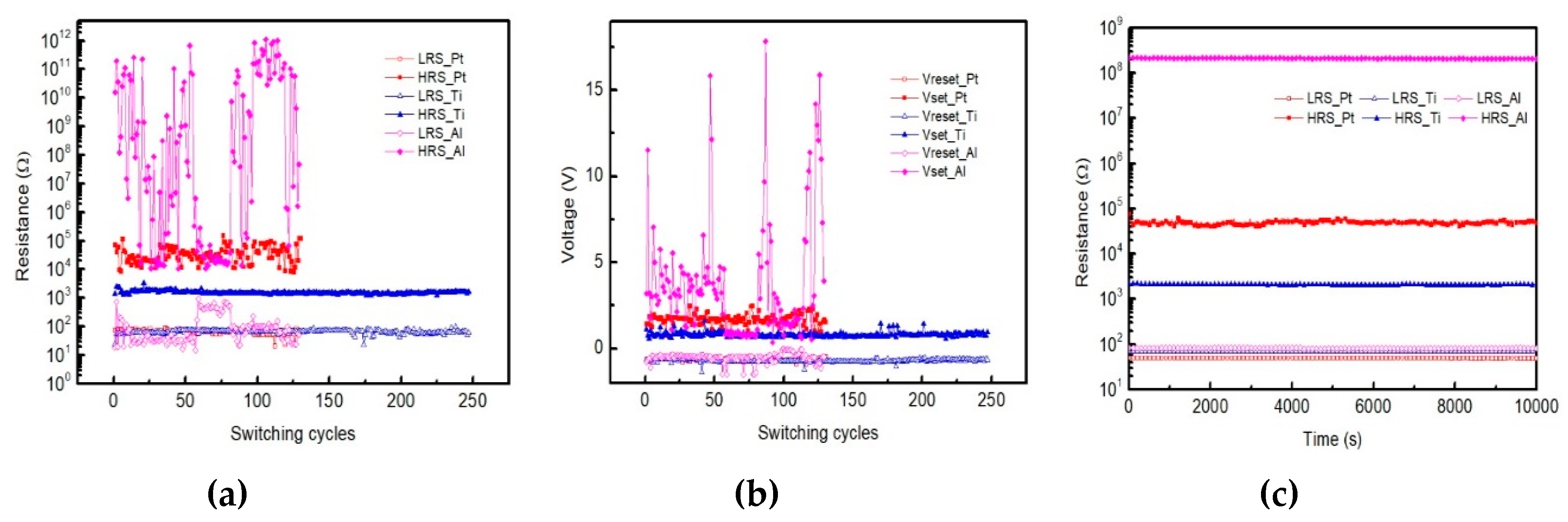
3. Results and Discussion

Figure 2a shows the morphology of the sputtered IGO thin film. According to the AFM analysis results, the sputtered film has a very small root-mean square value of 0.362 nm, which indicates that the sputtered thin film is smooth. The sputtered film is amorphous because the larger intensity only appears at about 25 degree which is attributed to the glass substrate and no sharp or distinctive peak showing up in the XRD patterns as shown in Figure 2c, indicating the lack of long-range crystalline order. Furthermore, Y. H. et al. have reported that amorphous films which have no grain boundaries not only favor high-speed electronic devices but also lead to better mobility of oxygen vacancies [25]. For the sake of the amorphous films, the resistive switching process of RRAM can be stabilized. Figure 2c shows the oxygen–metal bonding of the thin film from the XPS result. The O 1s peak was deconvoluted into three peaks at 530.2, 531.5, and 533.3 eV, which are assigned to the well-bonded oxygen with metal cation (M–O), oxygen vacancies (Vo), and metal hydroxide species (M–OH), respectively. Among all, the oxygen vacancies accounted for about 48.31% which indicates that the film has a proper amount of oxygen vacancies to form filaments when operated as an RRAM device.
When it comes to RRAM devices, we have extracted parameters—such as set voltage, reset voltage, high resistant state, and low resistant state—which are some of the basic parameters to quantify RRAM performance. The lifetime and the reliability will also be concerned to distinguish an RRAM is good or not. Since Pt is a kind of inert metal, which will not interact with the active layer, we first use Pt as TE to simply focus on the influence on the RRAM performance from the active layer itself before discussing the influence of different TE.
Figure 3a illustrates the IV sweep curve of the 10th, 50th, and 100th cycles of the IGO RRAM operated under bipolar switching mode. The IV sweep process can roughly divide into four parts. First, we applied a positive voltage increased from 0 V to 2.5 V to the TE and caused the RRAM to switch from HRS to LRS. Second, the applied positive voltage decreased back to 0 V and kept the RRAM at LRS. In the above two progress, which is so-called the set process, 5 mA current compliance was held in order to provide the device from hard-breakdown. Third, a negative reverse bias was applied from 0 V to −0.9 V to the TE and the RRAM will then be switched back to HRS. Finally, the applied reverse bias gradually decreased to 0 V while the RRAM kept at HRS. The latter two progress is what we called the reset process. When the whole four steps were conducted means that a sweep cycle was completed. During the measurement, the RRAM with TE of Pt was switched for 130 cycles and finally hard-breakdown. It is calculated from the 130 cycles that the average set voltage is 1.727 V, the average reset voltage is −0.596 V, the average HRS is 54,954.09 Ω, and the average LRS is 64.97 Ω, respectively. Since the maximum current of the reset process is corresponding to that of the set process, it is recognized that the resistive switching behavior of the RRAM with TE of Pt is dominated by the oxidation-reduction reaction. Figure 3b depicts the schematic of the redox mechanism. The oxygen ions migrate from the bottom of the switching layer to the top of the switching layer because of the electric field induced by the applied positive bias, which left oxygen vacancies behind. As the positive voltage increased, the oxygen vacancies accumulate and form a conductive filament, which turns the RRAM from HRS to LRS. Owing to Pt being an inert metal, the accumulative oxygen ions will not react with the Pt TE and may escape outward around the interface between the TE and active layer, which results in a thin filament.
After knowing some basic characteristics of the IGO RRAM with TE of Pt, we substituted Ti and Al for Pt as TE. The IV sweep curves are shown in Figure 4. Generally, the oxidation of both Ti and Al occur much easier than that of Pt. As a result, when the Ti and Al TE were deposited on the switching layer, both Ti and Al interacted with the oxygen ions in the switching layer because of their high activity to oxygen and formed TiOx and AlOx. However, as the TEM results shown in Figure 4c, TiOx has no clear boundary in TE while AlOx only appears at the interface between TE and active layer for about 6 nm as shown in Figure 4d. That is because oxygen ions diffuse more easily into the deeper Ti TE layer and form a thicker TiOx, which can be observed in the line scan profile as Figure 4e shows. In contrast, Figure 4d,f show the oxidized AlOx is much denser than TiOx. Once the AlOx layer formed at the interface, the oxygen ions are hard to diffuse into a deeper region of TE.
Different from Pt as TE metal, both Ti and Al will form an oxidation layer and further affect the conductive mechanism of the RRAM device. Figure 5 indicates the conductive mechanism of RRAM with Ti and Al. When a positive bias was applied to the Ti TE, the TiOx acted as a reservoir of oxygen ions, which assists to form sturdy filaments in the switching layer. Consequently, low set voltage and reset voltage are obtained. On the contrary, when a positive bias was applied to the Al TE, the reset process is distinguished from that of Ti. Since we already realized that the Al-O bond is hard to break, the rupture of the conductive filaments is then dominated by the Joule heat effect, which causes significantly higher current during the reset process than the set process as shown in Figure 4b. Besides, the oxidized AlOx layer is a good insulator, which may impede the forming of the conductive filaments. As a result, the conductive filaments may form through a different path in the switching layer thus higher set voltage and higher HRS can be obtained.
Lastly, we further discuss the characteristics of the IGO RRAM with different TE. Figure 6 shows the voltage versus switching cycles, resistance versus switching cycles and resistance versus time of the three RRAM devices in this work. Besides, some major parameters of the three devices are summarized in Table 1. The maximum average set voltage appears when TE is Al. This is due to the oxidized AlOx layer making the forming of the filaments more difficult in the switching layer. On the other hand, TiOx plays a role of reservoir which assists the forming of filaments therefore a minimum average set voltage is obtained. The minimum average reset voltage of −0.7 V appears when TE is Ti. This is due to the sturdy filaments forming with the assistance of the oxygen reservoir TiOx, so it needs a more negative bias to rupture the strong filaments. The significant large HRS and LRS can be observed with TE of Al is because of the Joule heat effect we have mentioned before. To analyze the stability of the RRAM devices, we defined the standard deviation (SD) of the set voltage, reset voltage, HRS, LRS using the formula
SD =   ( x x ¯ ) 2 n 1
where n is the total switching cycle, x is the value from each cycle, and x ¯ is the average of all cycles, respectively. All the standard deviations of the parameters are summarized in Table 1 as well. With small SD values, both Pt and Ti as TE show pretty good stability of set voltage, reset voltage, HRS, and LRS, which ensured the reliability of RRAM using Pt and Ti as TE. However, all the parameters we concerned show a great variation when the TE is Al. This result may be attributed to both a-IGO and dense AlOx. Unlike Pt and Ti, the conductive mechanism is dominated by Joule heat effect when using Al as TE, which may destroy the filament thoroughly and make the forming of filament more unstable. In addition, owing to the dense AlOx layer, the filaments are much more difficult to be formed, which means the possibilities of all the possible filament paths are almost the same. As a result, the amorphous thin film with TE of Al leads to a higher variation of set voltage and HRS while the different filament paths may have different set voltage and HRS. According to Figure 6c, all the three TE demonstrated good stability in the retention test, which means the RRAM devices all have the perfect capability to store data and keep the data quite stable.

4. Conclusions

In this work, IGO RRAM with three different TE of Pt, Ti, and Al were fabricated, and the characteristics were discussed. Because oxygen ions will diffuse into deeper Ti after deposited onto the switching layer, and the TiOx will form and assist the forming of filaments. As a result, the RRAM with TE of Ti shows the best reliability and stability with switching cycles of 247 times, the average set voltage of 0.811 V, the average reset voltage of 0.084 V, average HRS of 1621.81 Ω, average LRS of 63.93 Ω, respectively. On the other hand, the RRAM with TE of Al shows the worst stability because an approximately 6-nm-thick AlOx layer will form at the interface of TE and active layer, which makes filaments more unstable. All the three devices can maintain either HRS or LRS for over 10,000 s. In summary, IGO can serve as an excellent candidate for the RRAM device. Besides, with proper TE metal, the performance and reliability of IGO RRAM can be enhanced.

Author Contributions

Conceptualization, methodology, and writing—original draft preparation, W.-L.H. and Y.-Z.L.; Writing—review and editing, W.-L.H. and S.-P.C.; Supervision, S.-P.C.; Conceptualization and methodology, S.-J.C. All authors have read and agreed to the published version of the manuscript.

Funding

This research was funded by the Ministry of Science and Technology of the Republic of China under grant No. 107-2221-E-006-146.

Conflicts of Interest

The authors declare no conflict of interest.

References

  1. Chen, A. A review of emerging non-volatile memory (NVM) technologies and applications. Solid-State Electron. 2016, 125, 25–38. [Google Scholar] [CrossRef]
  2. Hegedus, J.; Elliott, S.R. Microscopic origin of the fast crystallization ability of Ge-Sb-Te phase-change memory materials. Nat. Mater. 2008, 7, 399–405. [Google Scholar] [CrossRef] [PubMed]
  3. Hu, J.M.; Li, Z.; Chen, L.Q.; Nan, C.W. High-density magnetoresistive random access memory operating at ultralow voltage at room temperature. Nat. Commun. 2011, 2, 8. [Google Scholar] [CrossRef] [PubMed]
  4. Meena, J.S.; Sze, S.M.; Chand, U.; Tseng, T.Y. Overview of emerging nonvolatile memory technologies. Nanoscale Res. Lett. 2014, 9, 33. [Google Scholar] [CrossRef] [Green Version]
  5. Bez, R.; Pirovano, A. Non-volatile memory technologies: Emerging concepts and new materials. Mater. Sci. Semicond. Process. 2004, 7, 349–355. [Google Scholar] [CrossRef]
  6. Khvalkovskiy, A.V.; Apalkov, D.; Watts, S.; Chepulskii, R.; Beach, R.S.; Ong, A.; Tang, X.; Driskill-Smith, A.; Butler, W.H.; Visscher, P.B.; et al. Basic principles of STT-MRAM cell operation in memory arrays. J. Phys. D Appl. Phys. 2013, 46, 20. [Google Scholar]
  7. Engel, B.N.; Akerman, J.; Butcher, B.; Dave, R.W.; DeHerrera, M.; Durlam, M.; Grynkewich, G.; Janesky, J.; Pietambaram, S.V.; Rizzo, N.D.; et al. A 4-mb toggle MRAM based on a novel bit and switching method. IEEE Trans. Magn. 2005, 41, 132–136. [Google Scholar] [CrossRef]
  8. Dong, X.Y.; Xu, C.; Xie, Y.; Jouppi, N.P. NVSim: A Circuit-Level Performance, Energy, and Area Model for Emerging Nonvolatile Memory. IEEE Trans. Comput.-Aided Des. Integr. Circuits Syst. 2012, 31, 994–1007. [Google Scholar] [CrossRef]
  9. Raoux, S.; Burr, G.W.; Breitwisch, M.J.; Rettner, C.T.; Chen, Y.C.; Shelby, R.M.; Salinga, M.; Krebs, D.; Chen, S.H.; Lung, H.L.; et al. Phase-change random access memory: A scalable technology. IBM J. Res. Dev. 2008, 52, 465–479. [Google Scholar] [CrossRef]
  10. Wang, W.J.; Shi, L.P.; Zhao, R.; Lim, K.G.; Lee, H.K.; Chong, T.C.; Wu, Y.H. Fast phase transitions induced by picosecond electrical pulses on phase change memory cells. Appl. Phys. Lett. 2008, 93, 3. [Google Scholar] [CrossRef]
  11. Julliere, M. Tunneling between ferromagnetic-films. Phys. Lett. A 1975, 54, 225–226. [Google Scholar] [CrossRef]
  12. Hudgens, S.; Johnson, B. Overview of phase-change chalcogenide nonvolatile memory technology. MRS Bull. 2004, 29, 829–832. [Google Scholar] [CrossRef]
  13. Akbari, M.; Lee, J.S. Control of resistive switching behaviors of solution- processed HfOx-based resistive switching memory devices by n-type doping. RSC Adv. 2016, 6, 21917–21921. [Google Scholar] [CrossRef] [Green Version]
  14. Akbari, M.; Kim, M.-K.; Kim, D.; Lee, J.-S. Reproducible and reliable resistive switching behaviors of AlOx/HfOx bilayer structures with Al electrode by atomic layer deposition. RSC Adv. 2017, 7, 16704–16708. [Google Scholar] [CrossRef] [Green Version]
  15. Lai, C.-H.; Chen, H.-W.; Liu, C.-Y. The Resistive Switching Characteristics in ZrO2 and Its Filamentary Conduction Behavior. Materials 2016, 9, 551. [Google Scholar] [CrossRef] [PubMed] [Green Version]
  16. Ha, S.; Lee, H.; Lee, W.Y.; Jang, B.; Kwon, H.J.; Kim, K.; Jang, J. Effect of Annealing Environment on the Performance of Sol-Gel-Processed ZrO2 RRAM. Electronics 2019, 8, 947. [Google Scholar] [CrossRef] [Green Version]
  17. Park, K.; Lee, J.S. Reliable resistive switching memory based on oxygen-vacancy-controlled bilayer structures. RSC Adv. 2016, 6, 21736–21741. [Google Scholar] [CrossRef] [Green Version]
  18. Shen, Z.J.; Qi, Y.F.; Mitrovic, I.Z.; Zhao, C.Z.; Hall, S.; Yang, L.; Kuo, T.; Huang, Y.B.; Zhao, C. Effect of Annealing Temperature for Ni/AlOx/Pt RRAM Devices Fabricated with Solution-Based Dielectric. Micromachines 2019, 10, 446. [Google Scholar] [CrossRef] [Green Version]
  19. Jeong, H.Y.; Kim, S.K.; Lee, J.Y.; Choi, S.-Y. Role of interface reaction on resistive switching of metal/amorphous TiO2/Al RRAM devices. J. Electrochem. Soc. 2011, 158, H979–H982. [Google Scholar] [CrossRef]
  20. Lee, K.J.; Chang, Y.C.; Lee, C.J.; Wang, L.W.; Wang, Y.H. 1T1R Nonvolatile Memory with Al/TiO2/Au and Sol-Gel-Processed Insulator for Barium Zirconate Nickelate Gate in Pentacene Thin Film Transistor. Materials 2017, 10, 1408. [Google Scholar]
  21. Son, J.Y.; Shin, Y.-H.; Kim, H.; Jang, H.M. NiO resistive random access memory nanocapacitor array on graphene. ACS Nano 2010, 4, 2655–2658. [Google Scholar] [CrossRef] [PubMed]
  22. Guo, Z.; Sa, B.; Zhou, J.; Sun, Z. Role of oxygen vacancies in the resistive switching of SrZrO3 for resistance random access memory. J. Alloys Compd. 2013, 580, 148–151. [Google Scholar] [CrossRef]
  23. Wu, Z.; Zhu, J. Enhanced Unipolar Resistive Switching Characteristics of Hf0.5Zr0.5O2 Thin Films with High ON/OFF Ratio. Materials 2017, 10, 322. [Google Scholar] [CrossRef] [PubMed] [Green Version]
  24. Li, Q.; Li, Y.H.; Gao, L.W.; Ma, F.; Song, Z.X.; Xu, K.W. Ru doping enhanced resistive switching behavior in InGaZnO thin films. RSC Adv. 2016, 6, 42347–42352. [Google Scholar] [CrossRef]
  25. Huang, Y.; Shen, Z.; Wu, Y.; Wang, X.; Zhang, S.; Shi, X.; Zeng, H. Amorphous ZnO based resistive random access memory. RSC Adv. 2016, 6, 17867–17872. [Google Scholar] [CrossRef]
  26. Rim, Y.S.; Choi, H.W.; Kim, K.H.; Kim, H.J. Effects of structural modification via high-pressure annealing on solution-processed InGaO films and thin-film transistors. J. Phys. D-Appl. Phys. 2016, 49, 6. [Google Scholar] [CrossRef]
  27. Huang, W.L.; Hsu, M.H.; Chang, S.P.; Chang, S.J.; Chiou, Y.Z. Indium Gallium Oxide Thin Film Transistor for Two-Stage UV Sensor Application. ECS J. Solid State Sci. Technol. 2019, 8, Q3140–Q3143. [Google Scholar] [CrossRef]
  28. Oshima, T.; Okuno, T.; Fujita, S. Ga2O3 thin film growth on c-plane sapphire substrates by molecular beam epitaxy for deep-ultraviolet photodetectors. Jpn. J. Appl. Phys. 2007, 46, 7217–7220. [Google Scholar] [CrossRef]
  29. Kokubun, Y.; Miura, K.; Endo, F.; Nakagomi, S. Sol-gel prepared beta-Ga2O3 thin films for ultraviolet photodetectors. Appl. Phys. Lett. 2007, 90, 3. [Google Scholar] [CrossRef]
  30. Kumar, S.; Soman, R.; Pratiyush, A.S.; Muralidharan, R.; Nath, D.N. A Performance Comparison Between beta-Ga2O3 and GaN HEMTs. IEEE Trans. Electron Devices 2019, 66, 3310–3317. [Google Scholar] [CrossRef] [Green Version]
  31. Yang, J.B.; Chang, T.C.; Huang, J.J.; Chen, Y.T.; Yang, P.C.; Tseng, H.C.; Chu, A.K.; Sze, S.M.; Tsai, M.J. Role of InGaOx resistive switching characteristics on the performances of resistance random access memory of Pt/IGO/TiN device. Thin Solid Film 2013, 528, 26–30. [Google Scholar] [CrossRef]
  32. Wang, X.T.; Qian, H.L.; Guan, L.; Wang, W.; Xing, B.R.; Yan, X.Y.; Zhang, S.C.; Sha, J.; Wang, Y.W. Influence of metal electrode on the performance of ZnO based resistance switching memories. J. Appl. Phys. 2017, 122, 5. [Google Scholar] [CrossRef]
  33. Hong, S.M.; Kim, H.D.; An, H.M.; Kim, T.G. Effect of Work Function Difference Between Top and Bottom Electrodes on the Resistive Switching Properties of SiN Films. IEEE Electron Device Lett. 2013, 34, 1181–1183. [Google Scholar] [CrossRef]
  34. Lee, C.B.; Kang, B.S.; Benayad, A.; Lee, M.J.; Ahn, S.E.; Kim, K.H.; Stefanovich, G.; Park, Y.; Yoo, I.K. Effects of metal electrodes on the resistive memory switching property of NiO thin films. Appl. Phys. Lett. 2008, 93, 3. [Google Scholar] [CrossRef]
  35. Lee, K.J.; Wang, L.W.; Chiang, T.K.; Wang, Y.H. Effects of Electrodes on the Switching Behavior of Strontium Titanate Nickelate Resistive Random Access Memory. Materials 2015, 8, 7191–7198. [Google Scholar] [CrossRef] [Green Version]
  36. Michaelson, H.B. The work function of the elements and its periodicity. J. Appl. Phys. 1977, 11, 4729–4733. [Google Scholar] [CrossRef] [Green Version]
Figure 1. Schematic of the InGaO RRAM structure.
Coatings 10 00504 g001
Figure 2. (a) AFM result of the sputtered IGO thin film. (b) XRD result of the sputtered IGO thin film. (c) XPS result of the sputtered IGO thin film.
Coatings 10 00504 g002
Figure 3. (a) IV sweep curve of IGO RRAM with TE of Pt. (b) The schematic of the redox mechanism with Pt TE. The blue circles present the oxygen vacancies and the white circles present the oxygen ions.
Coatings 10 00504 g003
Figure 4. IV sweep curve of IGO RRAM with TE of (a) Ti and (b) Al. Cross section from TEM result of IGO RRAM with TE of (c) Ti and (d) Al. Line scan profile of IGO RRAM with TE of (e) Ti and (f) Al.
Coatings 10 00504 g004
Figure 5. (a) Schematic of set and reset process of the IGO RRAM with TE of Ti. When a positive bias applied to the TE, the oxygen vacancies were arrayed by the induced electric field. With the aid of the TiOx layer, the set process is easier to approach. (b) The schematic of how Joule heat effect impact the filament when AlOx formed. Since the dense AlOx layer was formed, current crowding effect may happen at the interface between TE and IGO layer, which generate a large current and finally rupture the filament.
Coatings 10 00504 g005
Figure 6. Endurance test of the IGO RRAM with different TEs: (a) resistance versus cycles; (b) voltage versus cycles; (c) retention test of the IGO RRAM with different TEs.
Coatings 10 00504 g006
Table 1. Some parameters of IGO RRAM with TE of Pt, Ti, and Al
TESwitching CyclesAverage Vset (V)SD of Vset (V)Average Vreset (V)SD of Vreset (V)Average HRS (Ω)SD of HRS (Ω)Average LRS (Ω)SD of LRS (Ω)
Pt1301.7270.299−0.5960.07754,954.0931,622.7864.979.99
Ti2470.8110.139−0.70.0841621.81234.4263.938.14
Al1293.7493.543−0.5230.289~8 × 10¹⁰~2 × 1011145.3191.27

