Article

Self-Organized In-Depth Gradients in Highly Ti-Doped ZnO Films: Thermal Versus MW Plasma Annealing

by
Rehab Ramadan
1,2,
Ramón Fernández-Ruiz
3 and
Miguel Manso Silván
1,*
1
Departamento de Física Aplicada and Instituto de Ciencia de Materiales Nicolás Cabrera, Universidad Autónoma de Madrid, 28049 Madrid, Spain
2
Department of Physics, Faculty of Science, Minia University, Minia 61519, Egypt
3
Servicio Interdepartamental de Investigación, Universidad Autónoma de Madrid, 28049 Madrid, Spain
*
Author to whom correspondence should be addressed.
Coatings 2020, 10(4), 418; https://doi.org/10.3390/coatings10040418
Submission received: 31 March 2020 / Revised: 16 April 2020 / Accepted: 20 April 2020 / Published: 23 April 2020
(This article belongs to the Special Issue 1D, 2D and 3D ZnO: Synthesis, Characterization and Applications)

Abstract

:
Highly Ti-doped ZnO films have been produced by a spin-casting sol-gel process. The spin-casted films show high in plane homogeneity and optical quality. However, when inspected in depth, the surface composition is Ti rich. We show that two possible annealing processes can be considered depending on the properties to exploit. To promote in-depth homogenization, thermal annealing processes have been applied. Meanwhile, the gradients can be exacerbated, thanks to a non-negligible surface sputtering, by applying microwave (MW) plasma treatments with Ar discharges at different pressures. The microstructural properties of the differently processed films have been obtained prior to a study by grazing incidence X-ray fluorescence (GI-XRF) spectroscopy, which reveals the in-depth composition trends induced by the two alternative annealing procedures. The final wetting, electrical and optical properties of the films are described in accordance with the Ti distribution pattern revealed by GI-XRF. The study underlines for the first time how MW plasma annealing processes can be used to exacerbate self-induced atomic gradients in sol-gel films with potential implications in catalytic and biomedical applications.

1. Introduction

The applications of advanced materials have increasingly implied their deposition in the form of thin films in conjunction with their micro-nanostructuring. ZnO has been exposed to this trend in a wide range of applications, such as in photovoltaics [1], light-emitting devices [2], biosensors [3] or photocatalysis [4], which exploit the tunable light absorption and charge transfer properties of ZnO. From the point of view of processing, ZnO is an extremely flexible material with adapted protocols described for physical and chemical deposition techniques. The criticality is often determined by dopant elements that should tailor the desired properties; i.e., the charge transfer, light absorption, surface state, etc. As examples of doped ZnO deposition by physical techniques, Al-doped ZnO film synthesis has been achieved by using magnetron sputtering [5], while blue-emitting Er-doped ZnO films have been deposited by electron beam evaporation [6] or magnetic Co-rich ZnO was obtained by pulsed laser deposition [7]. In parallel, for the chemical techniques, Li- [8] and Ga- [9] doped ZnO deposition was described by the sol-gel process leading to highly oriented structures. Additional examples can be found of deposition of B-doped (n-type) ZnO by metal organic chemical vapor deposition [10] or Zr-doped ZnO by atomic layer deposition (ALD) [11].
Very often, the microstructural and functional properties of doped ZnO films are not final upon completion of the deposition process. Thermal annealing processes are frequently applied to refine the microstructure by promoting an increase of grain size leading to structures with increased band gap. On the other hand, post-deposition plasma treatments have been also applied to doped ZnO films with different aims. Oxygen plasma treatments applied to Ga-doped ZnO have been demonstrated to improve the electrical properties of the films and a sacrifice of the optical transmittance in the near- and mid-infrared ranges [12]. Paradoxically, inverse phenomena of deterioration of electrical properties and improvement of optical performance has been observed in oxygen plasma-treated Al-doped ZnO films [13]. On the opposite side to oxidative processes, H2 plasma treatments performed in between ZnO deposition cycles have been proposed to obtain ZnO:H. By increasing the number of H2 plasma treatments, a blue shift of the optical band gap was achieved [14]. Ar plasma treatments have been also applied to B doped ZnO films inducing a characteristic texture leading to an improvement of the open circuit voltage of hydrogenated Si solar cells [15]. Finally, combined Ar:H2 plasma processing has also induced an increase of the conductivity of Ti-doped ZnO (TZO) films and an improvement of the stability upon aging in air [16].
Ti doping has been considered an attractive way to induce tetravalent doping in ZnO with a minimal lattice distortion for the envisaged Zn substitution leading to an improved conductivity. Significant efforts have been devoted to optimize Ti doping by different techniques and at different doping levels. Although most reports refer to magnetron sputtering systems [17,18], chemical alternatives also exist, with an attractive control of the Ti doping level in a wide range of compositions demonstrated by the sol-gel process [19]. This latter work highlights that, the condensation of Ti-O within ZnO sols takes preferentially place at the film surface for Ti doping in the 1%–10% range. Such Ti-enriched surfaces are attractive to induce a covalent bonding stabilization of the films working in water solutions (i.e., for photocatalytic experiments or biomedical media). Nevertheless, the influence of the in depth properties shall be characterized in detail by appropriate profiling techniques.
Reflectivity studies and especially grazing incidence X-ray fluorescence (GI-XRF) have been used for decades for the characterization of thin films and other layered systems [20]. It is in fact a double purpose analytical technique providing, by working in total reflection conditions, quantitative elemental information and in-depth distribution. The elemental in-depth distribution is reconstructed from the analysis of evanescent waves associated to the different elements at different X-ray incidence conditions. The application of this technique to ZnO thin films has allowed determining the evolution of different out of plane processes. The progression upon thermal annealing of diffusion in ZnO buried interfaces [21] or the environmental effects induced by a simulated aging [22] were some of the first applications. More recently, the completion of magnetic ZnFe2O4 synthesis from ZnO/FeO multilayers by cation inversion [23] was confirmed using this technique. The identification of the in-depth Ga-dopant distribution in ZnO allowed establishing the homogenization of the dopant as the mechanism inducing an optical band-gap blue shift [24]. Finally, the techniques allowed also identifying the mechanism by which ZnO can eventually be forced to nucleate on self-assembled organothiols during ALD processes [25].
In the present work, we aim at identifying the in-depth distribution of highly Ti doped ZnO with a view in the evolution of this distribution upon different annealing treatments (thermal vs. microwave (MW) plasma) and in correlation with the final surface, optical and electronic properties. We point in particular for the first time to the possibility of mitigating or exacerbating these interface inhomogeneities in favor of particular desired properties.

2. Materials and Methods

2.1. Sol Gel Processing of Ti-Doped ZnO Thin Films

ZnO precursor was prepared from zinc acetate dihydrate (C2H6O4Zn·2(H2O), ≥98%, Sigma-Aldrich) diluted in ethanol at 0.2 M concentration. To allow the control of gelation, the same concentration of monoethanolamine diluted with ethanol was mixed with the first solution for stabilization [19]. The mixture was stirred under reflux for 10 h at 60 °C. TiO2 sol was prepared by dissolving 0.2 M of titanium isopropoxide (Ti[OCH(CH3)2]4 ≥98%, Sigma-Aldrich) in ethanol. We added 0.35 µl of HCl to the solution to induce an acid condensation catalysis [19]. Our study was performed with 5% Ti-doped ZnO solution (5% TZO) prepared by mixing aliquots of the previously described sols. The spin-casting technique was used to deposit the TZO sol on Si <100> and glass substrates previously cleaned by sequential ultrasonic baths for 5 min in trichloroethylene, acetone and ethanol. Deposition was carried out by casting 50 µl of the precursor and spinning at 2000 rpm spin speed for 30 s under N2 flow.

2.2. Annealing of Ti-Doped ZnO Thin Films

Spin-casted films were exposed to thermal annealing (TA) or microwave plasma annealing (MwPA). TA was performed at 200 °C or 300 °C for 30 min and MwPA in Ar at two different gas pressures (0.3 mbar and 0.7 mbar) was applied for 2 min after each spin casting step. The process of casting and subsequent annealing was repeated 5 consecutive times, except for the films prepared for XRF analysis, which were prepared with a single layer. For simplicity in the description of the samples, they are labelled as (TZt200 or TZt300) for TA films at 200 °C and 300 °C, respectively, and (TZp0.3 or TZp0.7) for MwPA films at 0.3 mbar and 0.7 mbar, respectively. Our home-made MwPA system was previously described [26].

2.3. Microstructural Characterization

Qualitative and quantitative composition analyses were performed by total-reflection X-ray fluorescence (TXRF) and GI-XRF. TXRF and GI-XRF data were acquired in a TXRF 8030C spectrometer from Atomika (Oberschleißheim, Germany), equipped with a 3 kW X-ray tube (Mo/W alloy anode with a double-W/C multilayer monochromator and a periodicity of 2d = 5nm) with an excitation energy of 17.4 keV (Mo Kα). A silicon drift detector (SDD) detector with an active area of 100 mm2 and a resolution better that 150 eV for 5.9 KeV (Ketek GmbH, Munich, Germany) was used. Additionally, the 8030c spectrometer is able to perform GI-XRF experiments around the critical angle. An offset of 3.5 mrad (0.2°) was measured in the spectrometer by comparing the theoretical critical angle of Si(100). The measurements were performed at 50 kV and the intensity was adjusted automatically so that a maximum count rate of about 8500 cps was achieved. Qualitative spectra were acquired during 500 s of acquisition time.
The effect of MwPA on the films’ morphology was evaluated by field-emission scanning electron microscopy (FESEM) using a Philips XL-40FEG operated at voltages below 10 kV. X-ray diffraction (XRD) studies were performed using a PANalytical X’Pert PRO THETA/THETA diffractometer in grazing-incidence configuration using Cu-Kα radiation (λ = 1.54 Å), a fixed incidence angle of 0.5° and 2° θ range from 10° to 60° with 0.04° increments and 10 s accumulation time. The equipment counts with an X-ray mirror for copper radiation, a parallel plate collimator, a flat pyrolytic graphite secondary monochromator and a Xe gas detector. The system was verified prior to the measurement of the batch of TZO films by measuring a sample of compacted Si microparticles (PANalytical) and verification of diffraction peak positions’ deviations within Δ2 θ ≤ ± 0.03°

2.4. Optical, Electrical and Wetting Characterization

The optical properties of TZO films were measured on films deposited on glass substrates using a V-560 double-beam spectrophotometer (Jasco, Easton, MD, USA), equipped with an integrating sphere to avoid scattering losses. The optical absorption was recorded in the ultraviolet–visible (UV–vis) range (250–900 nm). Tauc plots were obtained to compare the optical bandgap of TA and MwPA films.
The electrical performance of the TZO films was compared by electrochemical impedance spectroscopy (EIS) using by a Bio-Logic SP-150 system (Seyssinet-Pariset, France). The measurements were done after deposition of Au point contacts on the films by direct current (DC) sputtering. The alternating current (AC) impedance spectra were acquired in a Faraday cage between two surface electrodes up to 500 kHz frequency and applying a 0.5 V excitation potential. Fitting of data to electrical equivalent circuits was performed using the EC-Lab software from Bio-Logic Science Instruments (Seyssinet-Pariset, France).
The measurement of the water contact angle (WCA) on the different TZO films was performed in static mode using a KSW 100 with droplet volumes of 3 μL. The results are presented as the mean value of five WCA measurements on the each type of TZO film.

3. Results and Discussion

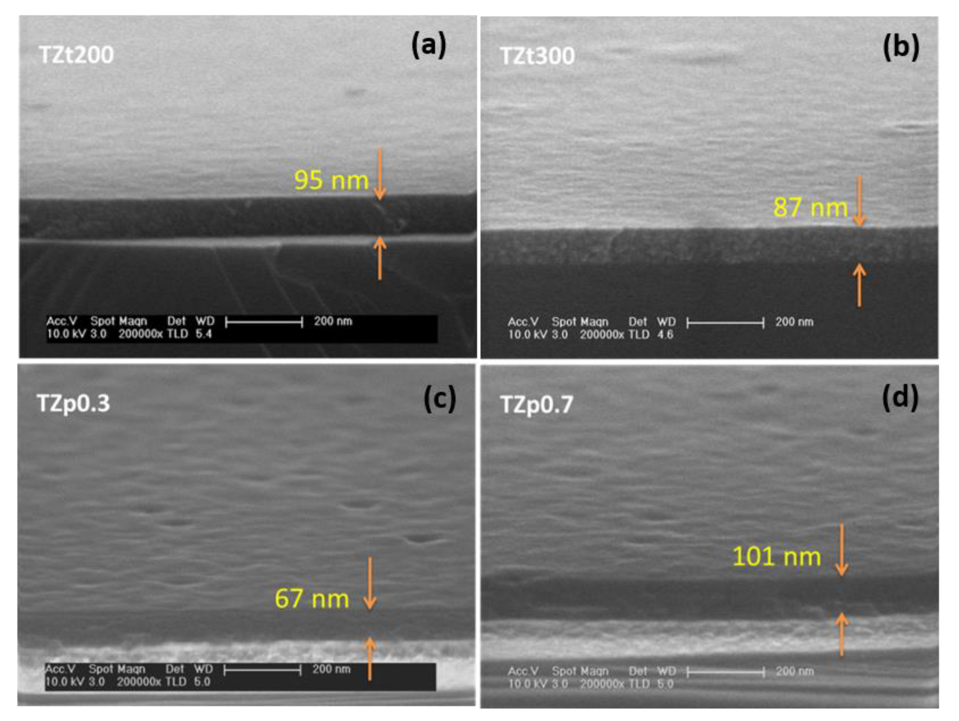
3.1. Thin Film Morphology

The analysis of Ti-doped ZnO thin films was performed after sequential deposition of 5 layers and application of the annealing process after each spin-casting cycle. Figure 1 shows the comparison between the films’ morphological structure subjected to TA at characteristic temperatures of 200 °C Figure 1a and 300 °C Figure 1b and films treated by MwPA at plasma pressures 0.3 Figure 1c and 0.7mbar Figure 1d. All films show good homogeneity with relatively flat surfaces and only soft wavy features with sizes below the wavelength of the visible range, which guarantee a good optical quality. The inspection of the total film thickness denotes a specific degree of condensation of the films related to their annealing conditions. Relevantly, the MwPA annealing treatments appear as the most drastic and less influential annealing treatments, respectively. However, the film annealed at 300 °C shows some granular structure, which is indicative of a more intense condensation and development of a nano-crystalline state [2]. It is convenient to remember that the MwPA process is influenced by both, a thermal component and an ion and electron surface bombardment that can induce surface sputtering. In this sense, in view of the granular microstructure, TZt300 appear as the most influential in the condensation of the TZO films. As regards the comparison of the two MwPA conditions, it is patent that the pressure reduction to 0.3 mbar is critical in providing a higher Ar ionization efficiency and energy per ion [27], which can contribute, besides a facilitation of desorption processes, to an enhanced thickness reduction.

3.2. Structural Properties

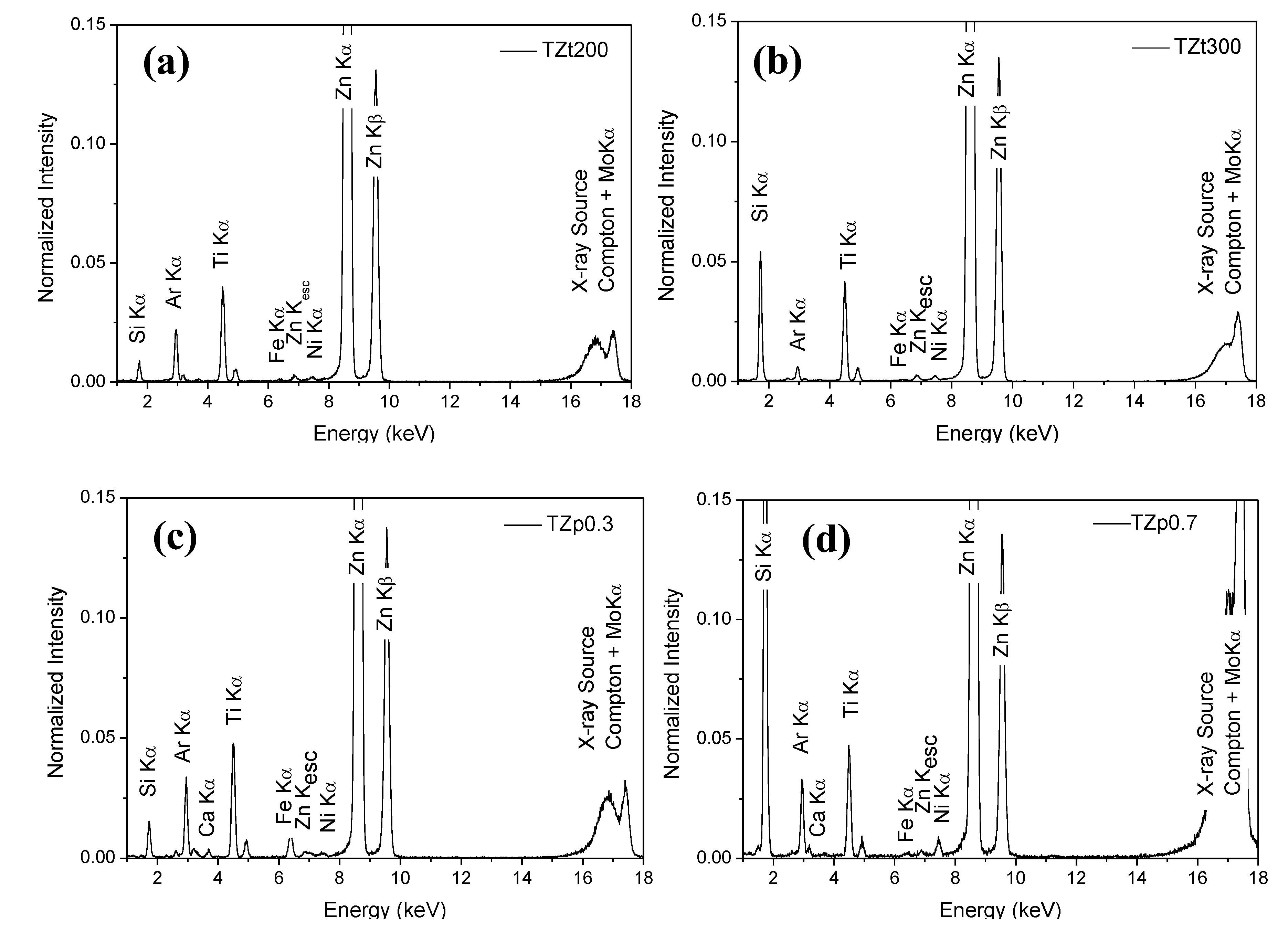
3.2.1. Total-Reflection X-Ray Fluorescence Spectrometry

The qualitative evaluation of the composition of the TZO thin films was made by acquiring TXRF spectra at incidence angles lower than the critical angle of the material on films prepared with only one spin casting/annealing cycle. Figure 2 shows the TXRF spectra of TZO thin films (5 at. % Ti to Zn) with different annealing conditions and normalized to Zn Kα signal: Figure 2a TA at 200 °C, Figure 2b TA at 300 °C, Figure 2c MwPA at 0.3 mbar and Figure 2d MwPA at 0.7 mbar.
TXRF spectra show the presence of Zn and Ti, as major elements and Ca, Fe and Ni, as traces with a maximum concentration of Fe and Ca of 1.2 wt% for the TZp0.3 film, which fall within the maximum specified by the supplier. There is also an Ar signal associated to air composition and a Si peak related to the Si(100) substrate. Spectra show strong variations of the Si signal, mainly in Figure 2d. The high intensity of the Si peak and Compton scattering and MoKα from the source can only be understood in terms of a higher incidence angle than the critical angle for total reflection in the TZp0.7 film. Relevantly, this film demonstrated a condensation rate well below the observed for the other samples (see SEM results). Since the critical angle for total reflection is proportional to the square root of the density of the material, this sample does not appear to comply with the rational critical angle during the experiment.
The calculated penetration curve (see a Figure A1) shows that the depth evaluated in the qualitative TXRF analysis was always lower than the first 5 nm of material except for the TZp0.7 film (Figure 2d), where the probing of the coating may have extended deeper due to a bad estimation of the film critical angle. In fact, the density of ZnO and other sol-gel thin films can be determined from the critical angle of incidence [28], which may require a specific calculus of the critical angle for this Ti-rich film. In fact, the theoretical TZO mass proportion, considering 5% of Ti on ZnO, was 6.22:100 for Ti:Zn, which implies an estimated mass proportion of Ti/Zn = 0.062. However, the experimental mass proportions obtained for the TXRF evaluation of the spectra of the investigated films (shown in Table 1) show a remarkable Ti super-stoichiometry.
Surface compositions are far from the theoretical composition and in all cases were always Ti rich. For TZt200 and TZt300 films the Ti enrichment was higher than 2 times the expected and for TZp0.3 and TZp0.7 films the enrichment was around 3 times higher. The results showed that the coatings, irrespective of the post-deposition treatment, were rich in Ti and indicated that the mechanism of formation of the gradient must have an origin in the deposition process. Additionally, the surface enrichment was higher in MwPA thin films, which can be explained in terms of the different sputtering yield of the two atoms in the final material. As illustrated in Appendix B, the sputtering of Zn is higher than for Ti in a wide range of energies for Ar ions impinging a simulated TZO film with 5 at.% Ti with respect to Zn. This is in agreement with the expected sputtering observed for Zn and Ti as induced by Ar ions [29] and explains the observed increase of relative Ti composition on the MwPA TZO samples

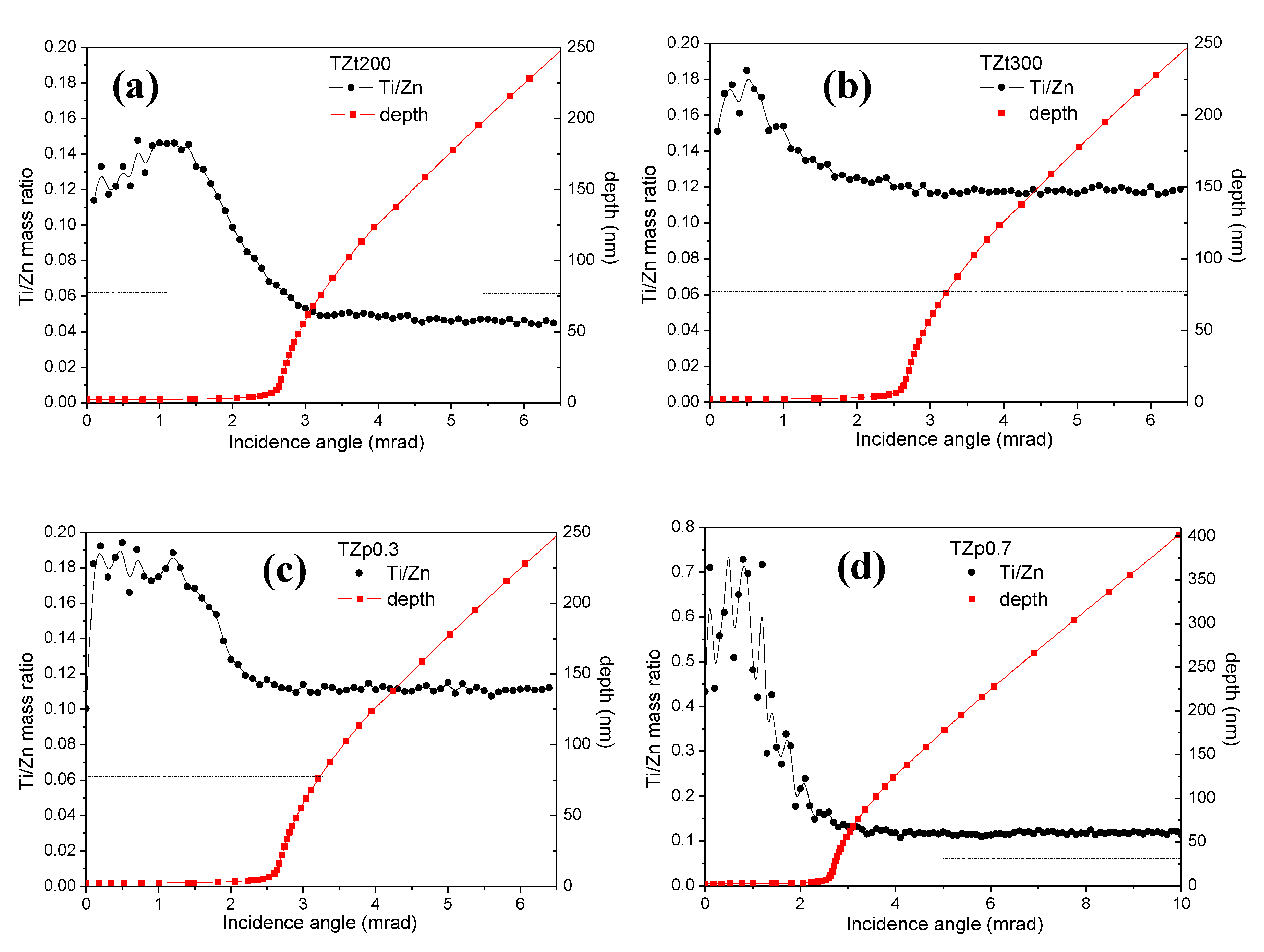
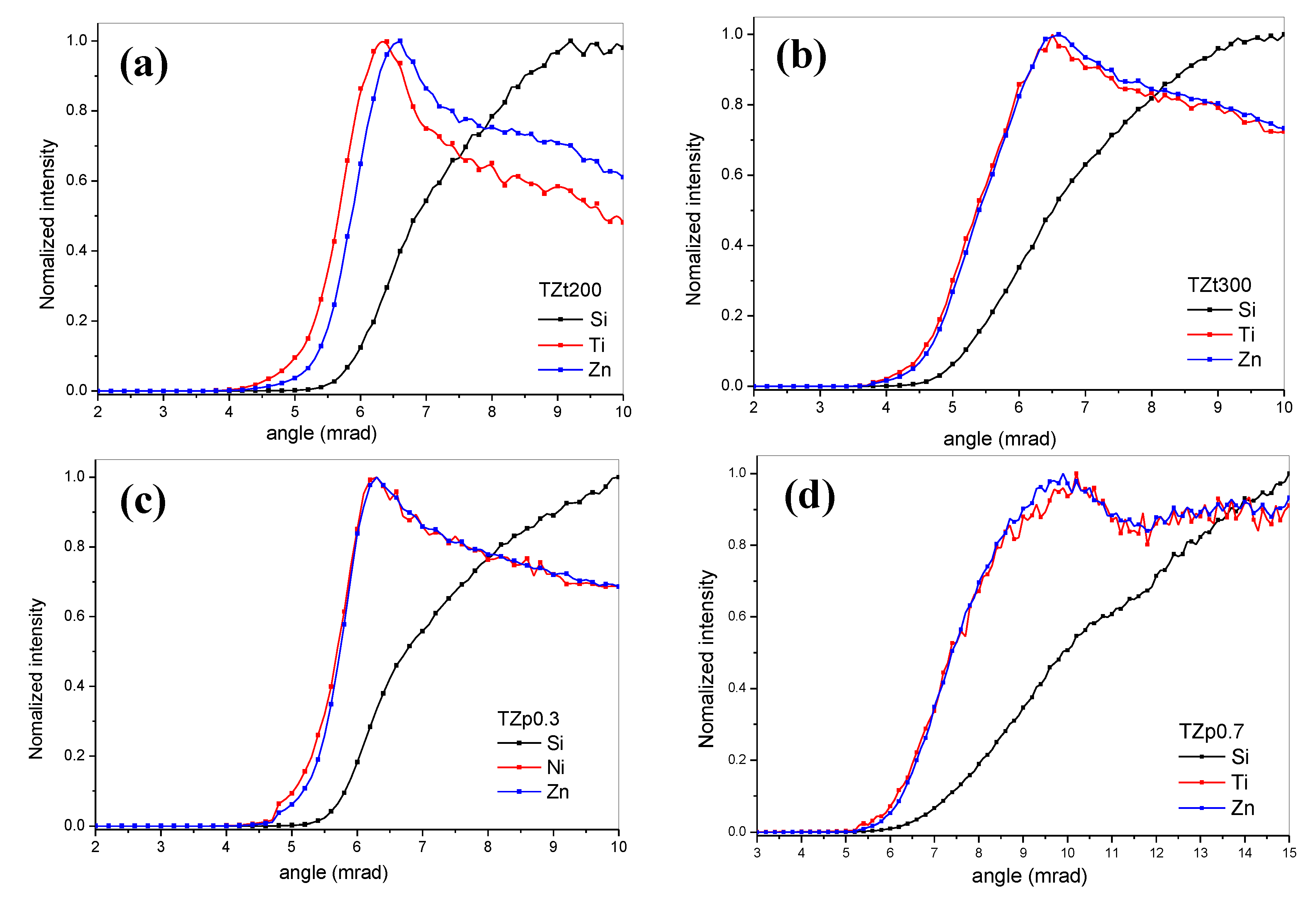
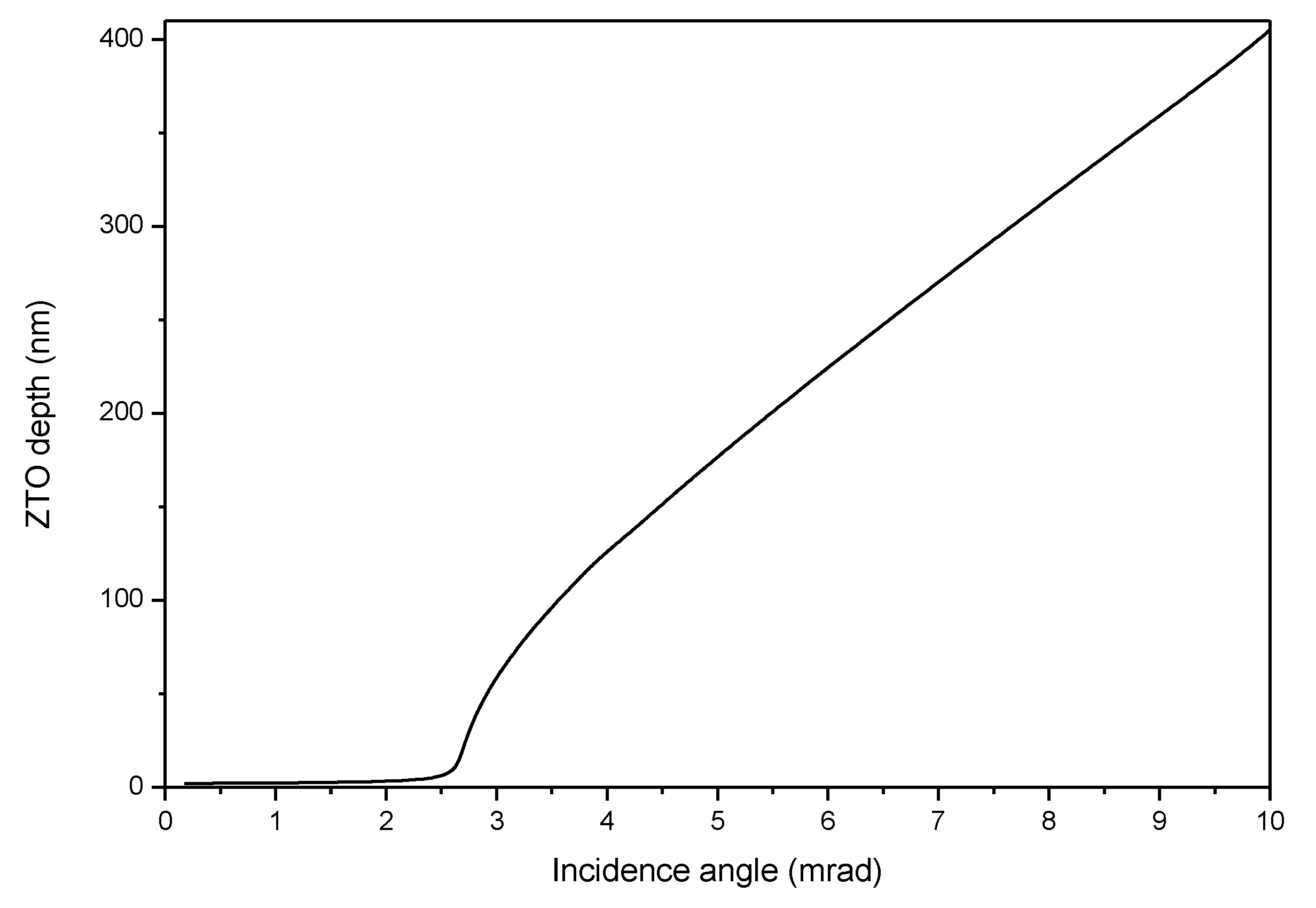
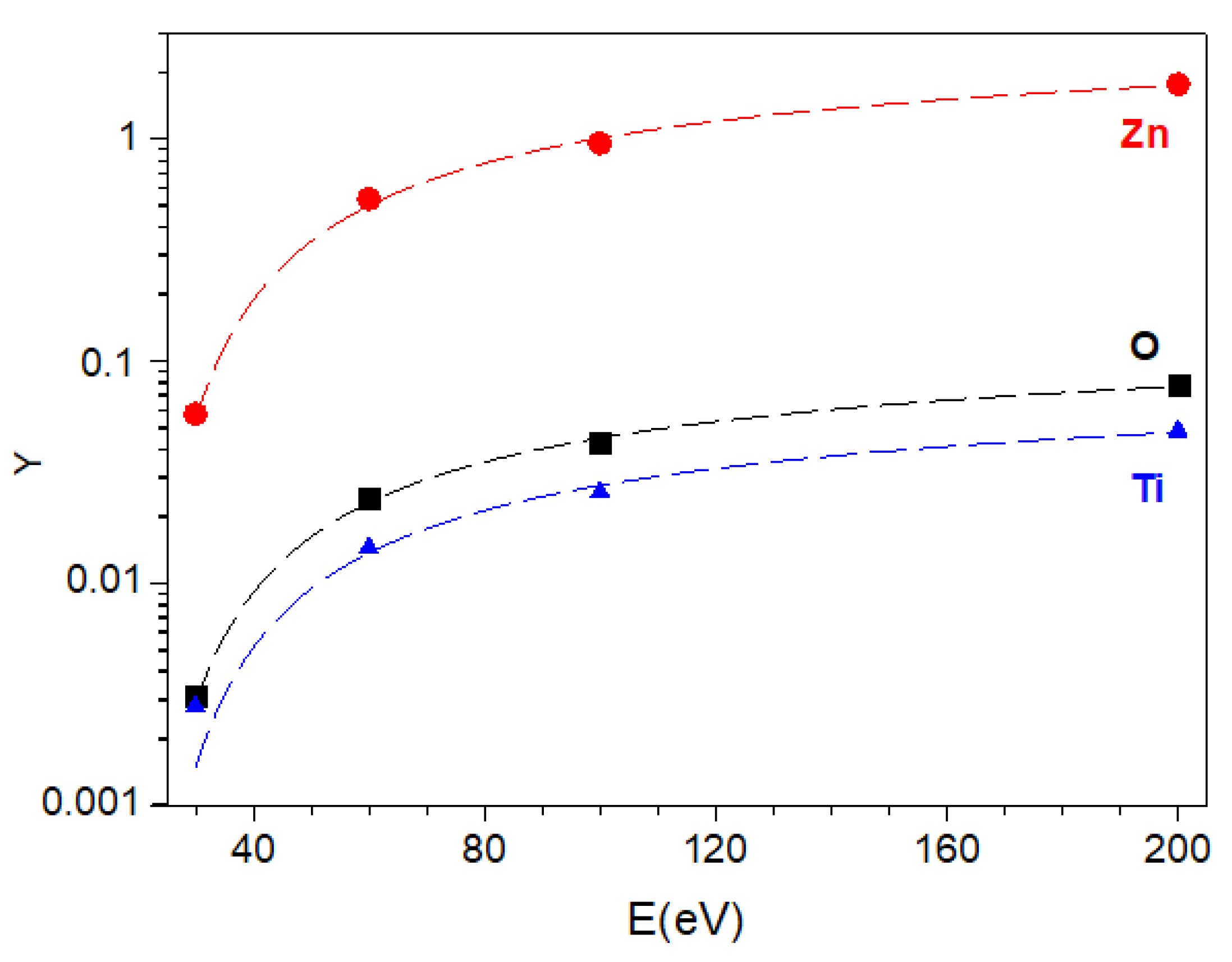
3.2.2. Grazing Incidence X-Ray Fluorescence Spectrometry

The K-line intensities of the elements Zn, Ti and Si were evaluated around the critical angle of the TZO material and Si(100) wafer. Lower angles imply information of the first depth nanometers and the depth of material inspected increases when the angle increases as shown in Figure 3.
A depth profile of the relative composition of Ti/Zn along the first hundreds of nanometers was obtained. Figure 3 shows, for each annealing condition, the Ti/Zn mass ratios obtained from the GI-XRF measurements from incidence angles between 0 to 6.4 with a step of 0.1 mrad (i.e., 64 spectra for each thin film). For all the films, a surface enrichment in Ti was observed around the first tens of nanometers. After this depth, the Ti/Zn mass ratio reached a plateau in all the cases. The horizontal dotted line displays the theoretical Ti/Zn mass ratio. For sample TZt200 (Figure 3a) the Ti/Zn mass ratio varied from 0.15 to 0.05 and for TZt300 (Figure 3b) the ratio varies from 0.18 to 0.12 from the surface to bulk, respectively. The gap was lower for the films annealed at 300 °C probably due to the highest activation of diffusion that tends to equilibrate the Ti/Zn ratio all over the surface. In any case, the Ti/Zn mass ratio measured for all concentrations was higher than expected, which confirms that the condensation process during spin coating is not homogeneous and more Ti than Zn was retained during xerogel film formation. There were also evident differences between TZp0.3 and TZp0.7 films as shown in Figure 3c,d, respectively. In both cases the Ti/Zn mass ratio was always higher than the expected value of 0.062. We can also observe a concentration gradient, with a Ti/Zn ratio higher at the surface and lower in the bulk. However, for the TZp0.3 film it varied from 0.19 to 0.11 while for the TZp0.7 film varies from 0.7 to 0.11. These results confirm on the one hand that the condensation process led to a preferred overall retention of Ti with respect to Zn. On the other hand, it becomes also clear that the plasma annealing induced an opposite trend to the TA, with an enhancement of the Ti stoichiometry on the surface with respect to the bulk. This can be again understood in terms of the difference in the sputtering yield of the different elements, which allows confirming that a preferential sputtering of Zn further accentuates the surface Ti/Zn atomic ratio unbalance.
Figure 4 shows the normalized intensity for the different film/substrate elements at different X-ray incidence angles. The results allow us to compare how the composition of Ti and Zn follow each other in terms of depth, and how their compositions evolve with respect to the Si substrate. The TZt200 film (Figure 4a) presents a remarkable mismatch between the increase of the surface Ti and Zn, making it possible to visualize the film as a real stack a TiO2 film doped with Zn (on the surface) and a ZnO film doped with Ti. This observation again emphasises the importance of the condensation process of the xerogel film during spin casting. After annealing at 300 °C (Figure 4b) such stack does no longer exist and although Ti is still over-stoichiometric, the evolution of the stoichiometry is much more homogeneous, as can be derived from a process that has notably activated diffusion (note the decreasing steepness of the normalized intensity curves). For the TZp0.3 film (Figure 4c) the steepness is high, although there is no shift between the curves suggesting a stacking. For the TZp0.7 film (Figure 4d), the steepness of the curves for both Ti and Zn is radically reduced, which suggests that the thermal activation effect at this pressure is higher than the one induced in the TZp0.3 film.

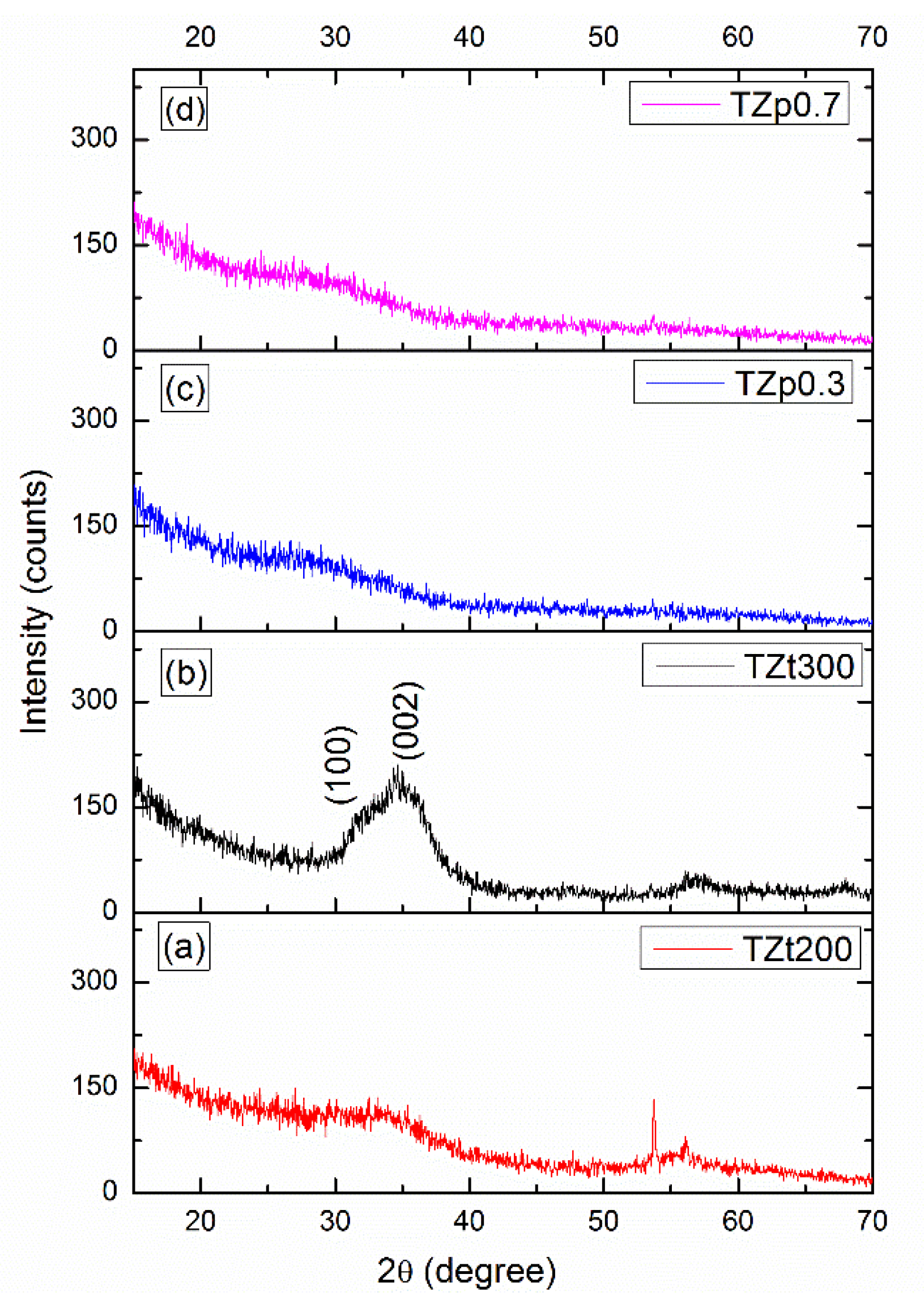
3.2.3. X-Ray Diffraction

The TZO films produced by 5 cycles of spin casting and annealed by the different processes were analyzed by XRD. The diffraction diagrams are shown in Figure 5 and denote, in general, the absence of a consolidated microstructure. In the case of TA films, the diagrams show some wide peaks for the TZt200 film (Figure 5a) but some additional emerging peaks for the TZt300 film (Figure 5b), which suggests a short range order organization.
The two peaks in the diagram of the TZt300 film are in agreement with the (100) and (002) peak assignments for ZnO crystals in a wurzite structure [2]. In any case, the lattice constriction effects induced by the high concentration of Ti dopant are responsible for an inhibition of the crystallization of ZnO for a given thermal activation, as previously observed [19]. This decrease in the crystal structure by TiO2 attributed to the higher activation energy required for the crystallization of TiO2 [30]. In fact, sol-gel ZnO films annealed at 200 °C have been observed to develop an incipient polycrystalline microstructure on Si substrates, which is consolidated after annealing at 300 °C [26,31]. Figure 5 shows that all the samples induced only an incipient crystallization with wide diffraction peaks denoting nanocrystalline phases. The diffraction diagrams from TZp0.3 (Figure 5c) and TZp0.7 (Figure 5d) present even wider peaks than the TA ones. Even though the peaks appear at positions which agree with the ZnO pattern (30–35 and around 56°), the wideness rather suggest a fully amorphous state for these TZO films.

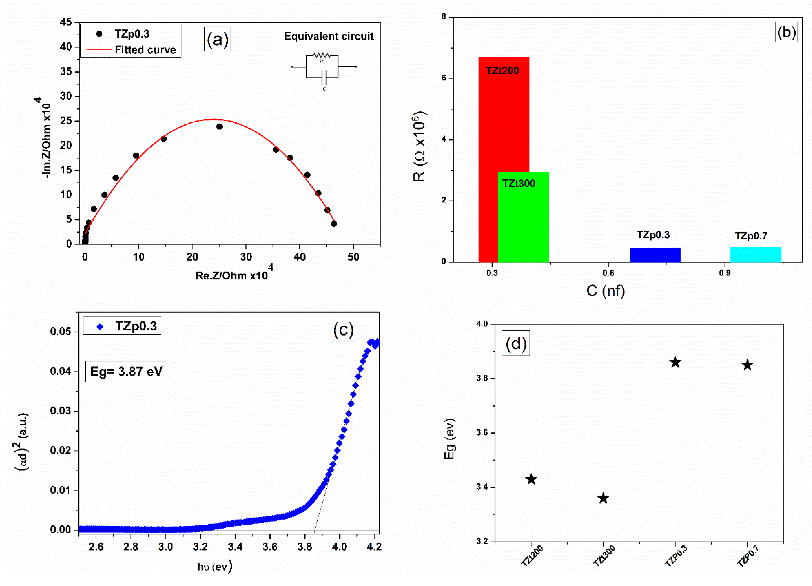
3.3. Electrical, Optical and Wetting Properties

A comparative study of the electrical properties of the TZO thin films with different annealing was performed by impedance spectroscopy. Figure 6a shows, as an illustrative example, the Nyquist plot for the TZp0.3 film with an indication of a resistance (R) and capacitor (C) in parallel equivalent circuit model. Such equivalent circuit was valid for all the studied films, which allowed obtaining by fitting an estimation of R and C for each film. An R vs. C map is presented in Figure 6b and shows the improvement in the electrical conduction for MwPA with respect to TA films as demonstrated by the decreasing resistance. We had previously shown that inclusion of Ti implies an increase in surface resistivity with respect to pure (TA) ZnO [19], so that a MwPA process can partially compensate for this drawback. This confirms the trend of reduced surface resistivity of MwPA samples for MwPA with respect to TA [26]. However, the MwPA-treated samples lead also to an increasing capacitive behavior.
In any case, while the resistance of MwPA films with respect to the best TA film (TZt300) decreases by a factor of 10, the capacitance increases only by a factor of 2–3. Since the general applications of TZO in optoelectronics imply operation in DC (photovoltaic cells), the results point to a favorable integration of MwPA TZO films conduction/extraction layer. In addition, the value of the optical bandgap for the transparent films was extracted by measurement of the UV–vis optical characteristics in the 250–900 nm wavelength range: transmission, from TZO films deposited on glass, and reflectance from TZO analogues deposited on Si (100). The data were transformed to obtain Tauc plots [32] and estimate the absorption coefficient (α). Moreover, assuming that TZO has a direct bandgap, the relationship between (α.d)2 and the photon energy (where d is the film thickness) was plotted to extract the optical bandgap (Eg). This was achieved by extrapolating the linear behavior at high energies to the horizontal line at (α.d)2 = 0, as indicated in Figure 6c (as an illustrative example for the TZp0.3 film). The curves presented in all cases a dual linear regime, which could be utilized to the determination of a double optical bandgap that can be observed in compounded semiconductors. For the TZp0.3 film, the first linear regime can be identified from 3.0 to 3.7 eV, while the second extends from 3.85 to 4.1 eV. Figure 6d shows the variation of the value of the highest Eg obtained for the four TZO films with the different annealing treatments. The results confirm the added value of the MwPA to induce higher Eg structures with respect to TA films [26], even with respect to temperatures of 400 and 600 °C [19]. The results obtained are in agreement with the physicochemical properties and suggest that the high doping level of Ti is able to maintain an amorphous/nanocrystalline structure of ZnO, which gives rise to high values of the optical bandgap. Meanwhile, the values obtained for TA films remain close to the standard for ZnO (3.37 eV), the values for the MwPA annealed samples increase higher than the values obtained for ZnO nanowires (3.65 eV) [33].
We further studied the wetting surface characteristics of the TZO films after the different annealing. Sessile droplet water contact angle measurements on the surfaces of the different TZO films are presented in Figure 7. As expected from the previously described physicochemical differences from TA and MwPA samples, the WCA of the surfaces were determined by the post-processing technique. Even though all the surfaces could be described as hydrophilic, TA induced higher contact angles close to 40°, with no clear differences between annealing at 200 and 300 °C. On the other hand, the MwPA surfaces presented lower contact angles with a reinforced hydrophilic character for the sample annealed at 0.3 mbar. Relevantly, such WCAs are similar to values obtained for Ar plasma processed anatase thin films produced by magnetron sputtering at similar pressures [34]. This observation supports the trend observed in MwPA TZO films, which consist of a Ti rich surface finishing.

4. Conclusions

In the present work, we demonstrate that the surfaces of sol-gel processed Ti-rich ZnO thin films exhibit from their casting an enrichment in Ti. Spin casting from sols containing 6.22 wt.% Ti with respect to Zn led to overall Ti contents higher than 14 wt.%. This phenomenon can be attributed to the fastest condensation catalysis of the Ti precursor with respect to the Zn precursor. Not only were the films enriched, but also there was an in-depth gradient with an acute surface enrichment in Ti that decreased smoothly to reach a stable composition after a few tens of nm. This surface enrichment in Ti can evolve differently depending on the post-processing technique selected to anneal the TZO films. In order to produce more homogeneous films, a TA at 300 °C can be applied. Inversely, one can exacerbate the surface enrichment in Ti by applying a MwPA process. At the particular pressure of 0.7 mbar, the preferential surface sputtering of Zn allowed defining the formation of a ternary compound (Ti/Zn mass ratio reaching 0.7) at the surface. For the compared post-processing conditions, the films exhibited rather amorphous (especially MwPA samples) or nanocrystalline microstructure (especially TA samples).
The post-processing techniques determined also different optical, electrical and wetting properties. The MwPA films exhibited lower surface resistivity (and slightly higher capacitance) in spite of a remarkable optical band gap (comparable to that of ZnO nanostructures) and behaved as highly hydrophilic surfaces. These results are extremely attractive for implementation of the thin films in photovoltaic devices (in view of the promising low resistivity) and for photocatalytic processes (featuring wide optical band gap and hydrophilic surfaces) ensuring high molecular affinity for the degradation of hydrophilic (polar) water pollutants.
This novel approach proposed to exacerbate the interface stoichiometric gradients self-generated during sol-gel processing may be attractive for a wide range of ternary ceramic thin films (i.e., composed of transition metal oxides such as Ti, Zr, Va, Ta, Sn, etc.) where surface properties may be optimized with respect to interface properties.

Author Contributions

Conceptualization, M.M.S. and R.F.-R.; methodology, M.M.S., R.R. and R.F.-R.; software, M.M.S., R.R. and R.F.-R.; validation, M.M.S., R.R. and R.F.-R.; formal analysis, M.M.S., R.R. and R.F.-R.; resources, M.M.S.; data curation, M.M.S., R.R. and R.F.-R.; writing—original draft preparation, M.M.S., R.R. and R.F.-R.; writing—review and editing, M.M.S., R.R. and R.F.-R.; visualization, M.M.S., R.R. and R.F.-R.; supervision, M.M.S., R.R. and R.F.-R.; project administration, M.M.S.; funding acquisition, M.M.S. All authors have read and agreed to the published version of the manuscript.

Funding

We are thankful for funding from the Ministry of Science, Innovation and Universities of Spain, through grant CTQ2017-84309-C2-2-R.

Acknowledgments

We greatly acknowledge the technical assistance of L. García Pelayo and I. Poveda during materials processing and characterization.

Conflicts of Interest

The authors declare no conflict of interest.

Appendix A

Figure A1 shows the simulation of the penetration depth curve as a function of incidence angle for a monochromatic MoKα X-ray beam (17.45 keV) irradiating a layer of ZnO (pZnO = 5.61 g cm−3) doped with 5% of Ti (pTi = 4.506 g cm−3) following the model of Slaboski et al. We considered a final material density (pTZO = 0.95pZnO + 0.05pTi) of 5.554 g.cm−3. Additionally, the X-ray optical constants of the TZO material were also calculated obtaining a scattering term δTZO = 3.55 × 10⁻⁶, an absorption term βTZO = 1.328 × 10−-7 and a critical angle for this material of αc = 0.153°.
Figure A1. Calculated depth penetration curve for the 5% doped TZO film composition considered in this work.
Coatings 10 00418 g0a1

Appendix B

Figure A2 shows the simulation of the sputtering yield for a TZO film with 5 at.% Ti and a density of 5.554 g·cm−3 for different energies up to 200 eV. The simulations were performed using a SRIM-2013 (Berlin, Germany) [35] to calculate the surface sputtering damage with Ar ions impinging in the normal direction to the film surface. The resulting sputtering yields (Y) for Zn, O and Ti were satisfactory fitted to a Bohdansky behaviour [29] in an extended energy range.
Figure A2. Simulated sputtering yield for Zn, O and Ti from a TZO film with 5 at.% Ti for a wide range of Ar ion energies. The simulated values (dots) are satisfactorily fitted to a Bohdansky behaviour (dashed line).
Coatings 10 00418 g0a2

References

  1. Jeong, J.A.; Park, Y.S.; Kim, H.K. Comparison of electrical, optical, structural, and interface properties of IZO-Ag-IZO and IZO-Au-IZO multilayer electrodes for organic photovoltaics. J. Appl. Phys. 2010, 107. [Google Scholar] [CrossRef]
  2. Gallach, D.; Munoz-Noval, A.; Torres-Costa, V.; Manso-Silvan, M. Luminescence and fine structure correlation in ZnO permeated porous silicon nanocomposites. Phys. Chem. Chem. Phys. 2015, 17, 20597–20604. [Google Scholar] [CrossRef] [PubMed] [Green Version]
  3. Zhao, Y.; Li, W.B.; Pan, L.J.; Zhai, D.Y.; Wang, Y.; Li, L.L.; Cheng, W.; Yin, W.; Wang, X.R.; Xu, J.B.; et al. ZnO-nanorods/graphene heterostructure: A direct electron transfer glucose biosensor. Sci. Rep. 2016, 6. [Google Scholar] [CrossRef] [PubMed] [Green Version]
  4. Makila, E.; Bimbo, L.M.; Kaasalainen, M.; Herranz, B.; Airaksinen, A.J.; Heinonen, M.; Kukk, E.; Hirvonen, J.; Santos, H.A.; Salonen, J. Amine Modification of Thermally Carbonized Porous Silicon with Silane Coupling Chemistry. Langmuir 2012, 28, 14045–14054. [Google Scholar] [CrossRef] [PubMed]
  5. Ghosh, S.; Sarkar, A.; Chaudhuri, S.; Pal, A.K. Optical-properties of zno—All films prepared by reactive dc magnetron sputtering. Vacuum 1991, 42, 645–648. [Google Scholar] [CrossRef]
  6. Zhang, X.T.; Liu, Y.C.; Ma, J.G.; Lu, Y.M.; Shen, D.Z.; Xu, W.; Zhong, G.Z.; Fan, X.W. Room-temperature blue luminescence from ZnO: Er thin films. Thin Solid Film 2002, 413, 257–261. [Google Scholar] [CrossRef]
  7. Kim, J.H.; Kim, H.; Kim, D.; Ihm, Y.E.; Choo, W.K. Magnetic properties of epitaxially grown semiconducting Zn1-xCoxO thin films by pulsed laser deposition. J. Appl. Phys. 2002, 92, 6066–6071. [Google Scholar] [CrossRef]
  8. Fujihara, S.; Sasaki, C.; Kimura, T. Crystallization behavior and origin of c-axis orientation in sol-gel-derived ZnO: Li thin films on glass substrates. Appl. Surf. Sci. 2001, 180, 341–350. [Google Scholar] [CrossRef]
  9. Fathollahi, V.; Amini, M.M. Sol-gel preparation of highly oriented gallium-doped zinc oxide thin films. Mater. Lett. 2001, 50, 235–239. [Google Scholar] [CrossRef]
  10. Chen, X.L.; Lin, Q.; Ni, J.; Zhang, D.K.; Sun, J.; Zhao, Y.; Geng, X.H. Textured surface boron-doped ZnO transparent conductive oxides on polyethylene terephthalate substrates for Si-based thin film solar cells. Thin Solid Film. 2011, 520, 1263–1267. [Google Scholar] [CrossRef]
  11. Lin, M.C.; Chang, Y.J.; Chen, M.J.; Chu, C.J. Characteristics of Zr-Doped ZnO Thin Films Grown by Atomic Layer Deposition. J. Electrochem. Soc. 2011, 158, D395–D398. [Google Scholar] [CrossRef]
  12. Lee, Y.L.; Chen, S.F.; Ho, C.L.; Wu, M.C. Effects of Oxygen Plasma Post-Treatment on Ga-Doped ZnO Films Grown by Thermal-Mode ALD. ECS J. Solid State Sci. Technol. 2013, 2, P316–P320. [Google Scholar] [CrossRef]
  13. Park, Y.S.; Seo, M.; Yi, J.; Lim, D.; Lee, J. Characteristics of aluminum-doped zinc oxide films with oxygen plasma treatment for solar cell applications. Thin Solid Film. 2013, 547, 47–51. [Google Scholar] [CrossRef]
  14. Uprety, P.; Macco, B.; Junda, M.M.; Grice, C.R.; Kessels, W.M.M.; Podraza, N.J. Optical and electrical properties of H-2 plasma-treated ZnO films prepared by atomic layer deposition using supercycles. Mater. Sci. Semicond. Process. 2018, 84, 91–100. [Google Scholar] [CrossRef]
  15. Krajangsang, T.; Hiza, S.; Hayashi, T.; Yunaz, I.A.; Hongsingthong, A.; Miyajima, S.; Konagai, M. Quantitative Analysis of Surface Morphology of Boron-Doped Zinc Oxide for Microcrystalline Silicon Solar Cells. Jpn. J. Appl. Phys. 2012, 51. [Google Scholar] [CrossRef]
  16. Wang, F.H.; Chao, J.C.; Liu, H.W.; Liu, F.J. Physical properties of TiO2-doped zinc oxide thin films: Influence of plasma treatment in H-2 and/or Ar gas ambient. Vacuum 2017, 140, 155–160. [Google Scholar] [CrossRef]
  17. Chung, J.L.; Chen, J.C.; Tseng, C.J. The influence of titanium on the properties of zinc oxide films deposited by radio frequency magnetron sputtering. Appl. Surf. Sci. 2008, 254, 2615–2620. [Google Scholar] [CrossRef]
  18. Yuste, M.; Escobar-Galindo, R.; Benito, N.; Palacio, C.; Martinez, O.; Albella, J.M.; Sanchez, O. Effect of the Incorporation of Titanium on the Optical Properties of ZnO Thin Films: From Doping to Mixed Oxide Formation. Coatings 2019, 180. [Google Scholar] [CrossRef] [Green Version]
  19. Ramadan, R.; Romera, D.; Carrascón, R.D.; Cantero, M.; Aguilera-Correa, J.-J.; García Ruiz, J.P.; Esteban, J.; Silván, M.M. Sol–Gel-Deposited Ti-Doped ZnO: Toward Cell Fouling Transparent Conductive Oxides. ACS Omega 2019, 4, 11354–11363. [Google Scholar] [CrossRef] [Green Version]
  20. Noma, T.; Miyata, H.; Ino, S. Grazing exit x-ray-fluorescence spectroscopy for thin-film analysis. Jpn. J. Appl. Phys. Part 2-Lett. 1992, 31, L900–L903. [Google Scholar] [CrossRef]
  21. Pagels, M.; Reinhardt, F.; Pollakowski, B.; Roczen, M.; Becker, C.; Lips, K.; Rech, B.; Kanngiesser, B.; Beckhoff, B. GIXRF-NEXAFS investigations on buried ZnO/Si interfaces. Nucl. Instrum. Methods Phys. Res. Sect. B 2010, 268, 370–373. [Google Scholar] [CrossRef]
  22. Jiang, H.; Chou, K.W.; Petrash, S.; Williams, G.; Thieme, J.; Nykypanchuk, D.; Li, L.; Muto, A.; Chen-Wiegart, Y.C.K. Environmentally induced chemical and morphological heterogeneity of zinc oxide thin films. Appl. Phys. Lett. 2016, 109. [Google Scholar] [CrossRef] [Green Version]
  23. Rodriguez, K.L.S.; Hoffmann, M.; Golmar, F.; Pasquevich, G.; Werner, P.; Hergert, W.; Torres, C.E.R. Producing ZnFe2O4 thin films from ZnO/FeO multilayers. Appl. Surf. Sci. 2017, 393, 256–261. [Google Scholar] [CrossRef]
  24. RoteIla, H.; Caby, B.; Menesguen, Y.; Mazel, Y.; Valla, A. Elemental depth profiling in transparent conducting oxide thin film by X-ray reflectivity and grazing incidence X-ray fluorescence combined analysis. Spectrochimica Acta Part B: Atomic Spectroscopy 2017, 135, 22–28. [Google Scholar] [CrossRef]
  25. Sampson, M.D.; Emery, J.D.; Pellin, M.J.; Martinson, A.B.F. Inhibiting Metal Oxide Atomic Layer Deposition: Beyond Zinc Oxide. ACS Appl. Mater. Interfaces 2017, 9, 33429–33436. [Google Scholar] [CrossRef]
  26. Ramadan, R.; Simiz, J.G.; Ynsa, M.D.; Silván, M.M. Microwave plasma annealing of sol-gel deposited tantalum oxide and zinc oxide films. Vacuum 2018, 149, 336–342. [Google Scholar] [CrossRef]
  27. Ramadan, R.; Abdelhady, K.; Manso-Silván, M.; Torres-Costa, V.; Martín-Palma, R.J. Microwave plasma and rapid thermal processing of indium-tin oxide thin films for enhancing their performance as transparent electrodes. J. Photonics Energy 2019, 9, 034001. [Google Scholar] [CrossRef]
  28. Veldhuis, S.A.; Brinks, P.; Stawski, T.M.; Gobel, O.F.; ten Elshof, J.E. A facile method for the density determination of ceramic thin films using X-ray reflectivity. J. Sol-Gel Sci. Technol. 2014, 71, 118–128. [Google Scholar] [CrossRef]
  29. Simon, A.H. Sputter processing. In Handbook of Thin Film Deposition, 4th ed.; Elsevier: Amsterdam, The Netherlands, 2018; pp. 195–230. [Google Scholar] [CrossRef]
  30. Deshmukh, H.; Shinde, P.; Patil, P. Structural, optical and electrical characterization of spray-deposited TiO2 thin films. Mater. Sci. Eng. B 2006, 130, 220–227. [Google Scholar] [CrossRef]
  31. Castanedo-Perez, R.; Jimenez-Sandoval, O.; Jimenez-Sandoval, S.; Marquez-Marin, J.; Mendoza-Galvan, A. Influence of annealing temperature on the formation and characteristics of sol-gel prepared ZnO films. J. Vac. Sci. Technol. A 1999, 17, 1811–1816. [Google Scholar] [CrossRef]
  32. Viezbicke, B.D.; Patel, S.; Davis, B.E.; Birnie III, D.P. Evaluation of the Tauc method for optical absorption edge determination: ZnO thin films as a model system. Physica Status Solidi (B) 2015, 252, 1700–1710. [Google Scholar] [CrossRef]
  33. Singh, J.; Kumar, P.; Hui, K.S.; Hui, K.N.; Ramam, K.; Tiwari, R.S.; Srivastava, O.N. Synthesis, band-gap tuning, structural and optical investigations of Mg doped ZnO nanowires. Crystengcomm 2012, 14, 5898–5904. [Google Scholar] [CrossRef]
  34. Kawakami, R.; Tominaga, K.; Okada, K.; Nouda, T.; Inaoka, T.; Takeichi, A.; Fukudome, T.; Murao, K. Etch damage characteristics of TiO2 thin films by capacitively coupled RF Ar plasmas. Vacuum 2010, 84, 1393–1397. [Google Scholar] [CrossRef]
  35. Ziegler, J.F.; Ziegler, M.D.; Biersack, J.P. SRIM—The stopping and range of ions in matter (2010). Nucl. Instrum. Methods Phys. Res. Sect. B-Beam Interact. Mater. Atoms 2010, 268, 1818–1823. [Google Scholar] [CrossRef] [Green Version]
Figure 1. Tilt angle field-emission scanning electron microscopy (FESEM) images of Ti-doped ZnO thin films composed of 5 layers with different annealing conditions. (a) thermal annealing (TA) at 200 °C, (b) TA at 300 °C, (c) microwave plasma annealing (MwPA) at 0.3 mbar and (d) MwPA at 0.7 mbar.
Coatings 10 00418 g001
Figure 2. Qualitative total-reflection X-ray fluorescence (TXRF) spectra of Ti-doped ZnO (TZO) thin films with different annealing conditions and normalized to Zn Kα signal. (a) TA at 200 °C, (b) TA at 300 °C, (c) MwPA at 0.3 mbar and (d) MwPA at 0.7 mbar.
Coatings 10 00418 g002
Figure 3. Depth profile of Ti/Zn mass ratios (black circles) and theoretical TZO depth curve (red squares) versus incidence angle of TZO thin films with different annealing conditions. The dotted line represents the theoretical Ti/Zn expected ratio. (a) TA at 200 °C, (b) TA at 300 °C, (c) MwPA at 0.3 mbar and (d) MwPA at 0.7 mbar.
Coatings 10 00418 g003
Figure 4. Grazing incidence X-ray fluorescence (GI-XRF) diagrams for Ti, Zn and Si from Ti-doped ZnO thin films with different annealing conditions. (a) TA at 200 °C, (b) TA at 300 °C, (c) MwPA at 0.3 mbar and (d) MwPA at 0.7 mbar.
Coatings 10 00418 g004
Figure 5. X-ray diffraction (XRD) diagrams for the 5 at.% Ti to Zn doped TZO films after different annealing processes: (a) TA at 200 °C, (b) TA at 300 °C, (c) MwPA at 0.3 mbar and (d) MwPA at 0.7 mbar MwPA processing.
Coatings 10 00418 g005
Figure 6. (a) Nyquist plot for the Ti-doped ZnO film after MwPA at 0.3 mbar with inset indication of the equivalent circuit model. (b) Resistance vs. capacity map for the different samples as extracted by fitting Nyquist plots to the equivalent circuit model. (c) Tauc plot for Ti-doped ZnO thin film after MwPA at 0.3 mbar. (d) Chart comparing the energy gap of the TA and MwPA films.
Coatings 10 00418 g006
Figure 7. Sessile drop water contact angle measurements performed on the surfaces of the TZO films after annealing: at 200 °C (TZt200), at 300 °C (TZt300), with MwPA at 0.3 mbar (TZp0.3) and with MwPA at 0.7 mbar (TZp0.7).
Coatings 10 00418 g007
Table 1. Surface composition of the TZO thin films obtained by TXRF working down to the critical angle of the TZO material. Elemental masses are expressed as relative mass units (rmu).
SampleTi (rmu)Zn (rmu)Ti/Zn
TZt20014.481000.14
TZt30014.841000.15
TZp0.317.521000.18
TZp0.717.001000.17

