Abstract
The luminescent properties of zinc oxide (ZnO) and nanostructured porous silicon (PSi) make these materials very appealing for photoemission applications. The current study reports on the fabrication of a composite of ZnO and nanostructured porous silicon micropatterns (ZnO + PSi micropatterns) onto heavily-doped silicon surfaces. The proposed composite micropattern is devoted to the future development of light-emitting diodes. The fabrication of the ZnO + PSi micropatterns was carried out in a two–step process. (1) A regular hexagonal micropattern of a photoresist/ZnO stack was fabricated by UV lithography on crystalline silicon substrates. (2) Before being lifted off the photoresist, nanostructured PSi micropatterns were fabricated by electrochemically etching the exposed areas of the silicon substrate. Subsequently, wet etching of the photoresist was carried out for the final development of the composite ZnO and PSi micropatterns. Further, thin films of ZnO and nanostructured PSi layers were characterized. In particular, their photoluminescent properties were analyzed, as well as their morphology and composition. The experimental PL results show that the ZnO layers have emission broadbands centered at (2.63 eV, blue), while the PSi layers show a band centered at (1.71 eV, red). Further, the emission peaks from the PSi layers can be tuned by changing their fabrication conditions. It was observed that the properties of the ZnO thin films are not influenced by either the surface morphology of PSi or by its PL emissions. Therefore, the PL properties of the composite ZnO + PSi micropatterns are equivalent to those featuring the addition of PSi layers and ZnO thin films. Accordingly, broadband optical emissions are expected to arise from a combination between the ZnO layer (blue band) and PSi (red band). Furthermore, the electrical losses associated with the PSi areas can be greatly reduced since ZnO is in contact with the Si surface. As a result, the proposed composite micropatterns might be attractive for many solid-state lighting applications, such as light-emitting diodes.
1. Introduction
The many useful physico–chemical properties of zinc oxide (ZnO) can be exploited in various potential applications [1], for instance, in optoelectronic applications for the fabrication of efficient photo-detectors [2], light-emitting diodes [3], and photovoltaic devices [4], or even in the field of biomedical sensing [5]. ZnO is a well-known luminescent material [6]. Usually, its photoluminescence (PL) spectrum has UV band emissions centered at 3.3 eV, which represents the typical bandgap (Eg) of ZnO thin films [7,8]. However, in some cases, a blueshift in the position of the emission band or in the presence of another visible blue broadband occurs. In more detail, the reduction in the Eg of ZnO thin films depends on the size of the nanocrystals and their shape [9,10,11].
The red emission from porous silicon (PSi) layers was first observed by Canham [12]. The particular position of the emission band depends on the Si crystal size [13]. An increase in the effective Eg of the PSi layer is attributed to a decrease in the Si crystallite size [14]. ZnO has been widely investigated in different structural forms on porous silicon templates [15,16]. The growth of ZnO thin films on PSi surfaces results in a notable enhancement in the PL properties of the composite, as previously reported [15,17,18]. However, PSi has lower electrical conduction than Si, which leads to limited conduction through optoelectronic devices [19,20]. Thus, the objective of the present work is to combine PSi and ZnO thin films to enhance PL emission properties and at the same time preserve electrical conduction.
In the present study, the morphology and bandgap of ZnO thin films and PSi layers were determined from the experimental PL spectra. Afterwards, regular hexagonal thin film structures of ZnO were grown on crystalline Si substrates. PSi nanostructures were subsequently fabricated in the Si areas between the hexagonal ZnO micropatterns, leading to ZnO and nanostructured PSi composite micropatterns. These structure are of interest in the development of optoelectronic devices for two main reasons. (1) The PL emissions can be enhanced by combining blue emissions from the ZnO micropattern with red emissions from the PSi nanostructures. (2) The electrical losses associated with the PSi areas can be greatly reduced since ZnO is in contact with the Si surface.
2. Materials and Methods
2.1. ZnO Thin Film Deposition
Electron beam evaporation was used to grow ZnO thin films on crystalline boron-doped silicon <100> substrates, with resistivity of 0.8–2 Ω·cm. The area of the samples was 1.5 cm × 1.5 cm. The source material was ZnO (99.9%), which was purchased from the Kurt J. Lesker Company. The typical base pressure was 2 × 10⁻⁷ Torr, which grew to 1 to 2 × 10⁻⁵ Torr during the evaporation process that was carried out without introducing any reactive gases in the deposition chamber. The e-beam emission current was 20 mA, and the deposition time was 30 min. The films possessed a brownish color after evaporation. For this reason, to improve the optical transparency of the ZnO thin films, thermal annealing at 350 °C was carried out in an air atmosphere for 30 min.
2.2. Fabrication of ZnO Micropatterns by UV-Lithography
The surface micropatterns of ZnO thin films were fabricated using a photolithographic technique with a negative photoresist (Ariston 20 series). The photoresist was deposited by spin casting, where the spin time was 30 s, and the spin speed was 3000 rpm. Afterwards, the deposited photoresist was dried on a hot plate at 70 °C for 15 min. The photoresist/ZnO stack layers were then exposed for 3 min to UV radiation (Hamamatsu LC-L1 UV–led spotlight source, 1 W.cm−2) through a hexagonally-structured photomask. Before the lift-off step of the photoresist micropattern, nanostructured porous silicon was fabricated on the exposed silicon areas among the photoresist/ZnO micropattern, as explained in the next subsection. Subsequently, the photoresist was developed by immersing the sample in 0.25 M of NaOH for 1 min, followed by wet etching of ZnO residuals in HF/H2O (1:20) solution for 10 s.
2.3. Fabrication of Spongy Nanostructured PSi
Photoresist/ZnO-micropatterned stacks were used for electrochemical etching of the exposed silicon areas. The samples were mounted in a sample holder with an active area of 1.23 cm2 and then exposed to the etching solution. The etching solution consisted of a (1:4) mixture of HF (48%)/ethanol (99%). The applied current density was 8 mA/cm2, and the etching time was 100 s, leading to sponge-like nanostructures. The composite ZnO + PSi micropatterns were developed after lifting the samples off the photoresist in acetone for 1 min. Finally, the samples were cleaned using ethanol, followed by distilled water, and were finally dried with nitrogen steam. A schematic representation of the fabrication process is shown in Figure 1.
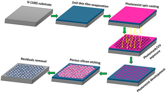
Figure 1.
Schematic representation of the steps followed for the fabrication of the ZnO + PSi composite micropatterns on silicon substrates.
2.4. Characterization Techniques
Photoluminescence measurements were carried out using a spectrofluorometer (SLM-Aminco Bowman AB2 series, Rochester, NY, USA) provided with a 150 W Xe lamp for excitation. Photoluminescence emissions were collected at a 90° angle from the excitation beam.
The morphology of the thin films was studied by field emission scanning electron microscopy (FESEM, XL-40 FEG, Philips, Eindhoven, The Netherlands) operated at 10 kV. An energy dispersive spectroscopy X-ray analyzer (EDX, Inca X-sight 7558, Oxford Instruments, London, UK) coupled to the microscope was used to determine the elemental compositions of the films in addition to composition mapping.
3. Results and Discussion
3.1. Photoluminescence Properties of PSi and ZnO Layers
Photoluminescence (PL) is a very useful tool for the study of the electronic and optoelectronic properties of materials since PL spectra are intimately related to the band structure of semiconductors and nanostructures [21]. In this work, photoluminescence spectroscopy was used to study the light emission properties of PSi and ZnO layers to determine the bandgap of these materials. Figure 2 shows the PL spectra in the 400–750 nm wavelength range of the ZnO and PSi layers, which were taken using an excitation wavelength of 225 nm (UV excitation). Since both the PSi and ZnO layers were grown onto silicon substrates, the experimental PL data were normalized to the silicon spectrum.
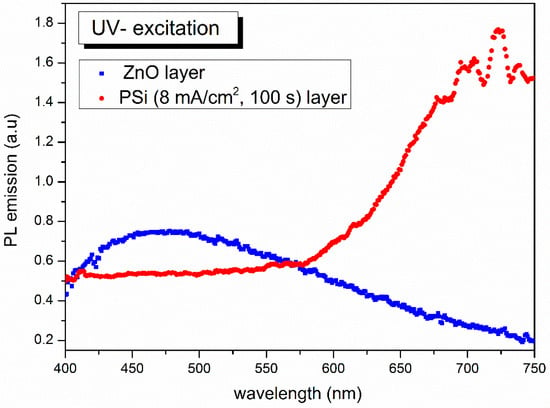
Figure 2.
PL emission spectra from a typical ZnO thin film and a PSi layer under UV excitation at 255 nm.
Thin films of ZnO typically show an allowable bandgap transition in the 3 to 3.3 eV (375–410 nm) interval, depending on the film thickness and the specific treatment after deposition [22,23]. In the case of ZnO nanostructures, including ZnO nanowires, nanorods, and nanobelts [9,10,11,24], a blueshift in the emission band of the PL spectra was previously reported, as well as the presence of an additional higher broadband emission centered between 2 and 3 eV [10,11]. Overall, a decrease in the bandgap occurs, which depends on the size and shape of the nanostructure.
In the current study, a broad emission band centered at 470 nm (2.63 eV) was observed for the thin layers of ZnO, which is the value of the bandgap. This band might be associated with the presence of oxygen vacancies in the ZnO layer, as already reported by many authors [15,25,26]. The broad shape of this band could be due to a number of factors, including inhomogeneous thin layer thickness, composition, nanocrystal size, and variation in the stoichiometry of the ZnO thin films. All or part of these effects might also be responsible for the reduction in the bandgap value to 2.63 eV. Another mechanism might be responsible for the narrowing of the bandgap of ZnO. As previously reported [27], the visible emissions from micro- and nano-crystalline ZnO are attributed to a transition from photogenerated electrons in the conduction band to a deeply trapped hole in the valence band, which effectively reduces the band gap value of ZnO micro- and nano-structures. The characteristic morphology of the ZnO thin films is shown in the top-view FESEM image of Figure 3a, and a magnified cross- sectional image is shown in Figure 3b, which confirms the small size of the ZnO nanocrystals and the presence of some cavities in the layer due to this small thickness, where the typical crystal size is estimated to be around 30–40 nm.
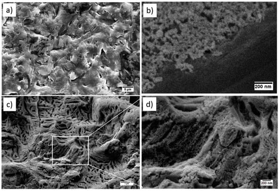
Figure 3.
FESEM images: (a) a top-view of the ZnO layer, (b) a cross-sectional view under a higher magnification of a defined area in the ZnO film, (c) top-view of the PSi layer prepared at an 8 mA/cm2 current density, and (d) a higher magnification top-view image of a defined area in the PSi layer.
Additionally, the PSi layers show several emission peaks in the 690 to 740 nm wavelength range, with the main one centered at 725 nm. The origin of light emissions from the PSi nanostructures is generally attributed to two types of luminescence mechanisms, namely the manifestation of quantum confinement effects and the presence of radiative defects in the thin films [28].
PSi is usually described as a material composed of Si nanocrystals embedded in an amorphous matrix [29,30]. A typical structure is shown in Figure 3c. Additionally, a magnified image is shown in Figure 3d. Using the Imagej software package, the pore diameter of the fabricated PSi nanostructures was calculated to be in the range of 20–50 nm for the spherical nano-holes and was larger, in the range of 75–200 nm, for the linear cracks. Accordingly, the PL emission in the visible is attributed to quantum confinement in the nanocrystals, which results in an increased bandgap value compared to that of bulk Si (1.12 eV) [31]. An increase in porosity results in a reduction of the size of the Si nanocrystals, which results in a band position blueshift, and vice versa [15]. In our case, the emission band was located in the red region of the visible spectrum and centered at 1.71 eV. This result is in a good agreement with previously reported studies on silicon quantum dots and porous silicon [13,28].
3.2. ZnO + PSi Surface Micropatterns
To fabricate ZnO + PSi micropatterns, regular hexagonal thin film structures of ZnO (line widths—190 µm) were grown on crystalline Si substrates. Spongy PSi nanostructures (shown in Figure 3c) were subsequently fabricated by electrochemically etching the exposed Si areas between the ZnO micropatterns. FESEM combined with EDX were used to determine the elemental composition map of the ZnO + PSi surface micropatterns. The results are presented in Figure 4. An interwoven image of all the elemental composition of the system is shown in Figure 4b. In detail, Figure 4c–e displays the Zn, O, and Si surface distributions. Map 4d shows that the largest percentage of O atoms is located in the ZnO film areas due to the oxygen vacancies in the ZnO layer, as discussed in Section 3.1. These results show that the ZnO and PSi areas are well defined with minimal mixing. This will help avoid any influence of one material on another for photoluminescence, as is the case for ZnO-infiltrated PSi films [32].
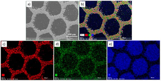
Figure 4.
(a) FESEM image of the nanostructured ZnO + PSi micropatterns, (b) EDX complementary map of Zn, O, and Si distribution in the ZnO + PSi layer; (c–e) indicate the EDX maps for Zn, O, and Si, respectively.
Figure 5 shows a semiquantitative EDX analysis of the ZnO+PSi micropatterns. In particular, Figure 5a shows the elemental composition in a spot taken from the PSi area, and Figure 5b focuses on an area in the ZnO micropattern. The practical results confirm that, as expected, Si and O are the main elements composing the PSi layer, whereas Si, O, and Zn are the main elements of the ZnO micropattern layer. In the latter case, the Si signal comes from the underlying Si substrate. This fact confirms the small thickness of the ZnO layers. Furthermore, the films show good compositional homogeneity and are free from contamination.
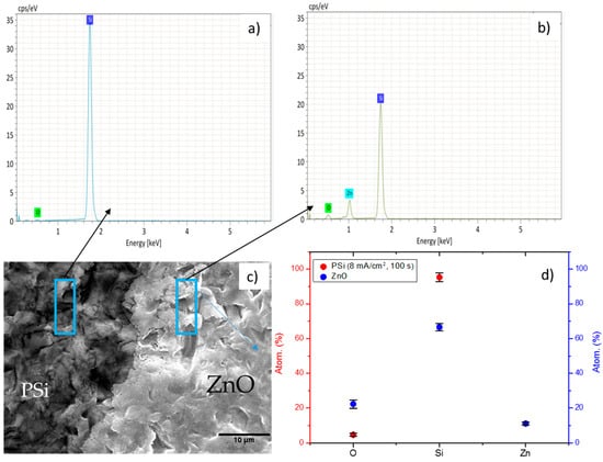
Figure 5.
EDX microanalysis of the elemental composition of the ZnO + PSi micropattern sample: (a) EDX analysis of the PSi layer, (b) EDX analysis of the ZnO micropattern layer, (c) FESEM top-view image of the two structures, and (d) a chart comparing the variations of the atomic percentage of the main elements in the PSi and ZnO micropattern layers.
Figure 5c shows a typical FESEM image of the two regions of the sample under study, highlighting the different morphologies of PSi and ZnO. The atomic percentages of Si, O, and Zn in the two regions of the ZnO + PSi micropatterns are presented in Figure 5d. Since PSi can be described simply as an amorphous homogeneous matrix of Si nanocrystals and air, its main elements are Si and O [31]. Furthermore, the atomic percentage variations shown in Figure 5d are consistent with the surface composition maps in Figure 4c–e.
4. Conclusions
The luminescent properties and morphology of ZnO thin films and nanostructured porous silicon (PSi) layers were analyzed by a combination of photoluminescence (PL) spectroscopy, scanning electron microscopy (SEM), and energy dispersive X-ray (EDX) analysis. The experimental PL spectra show blue broadband emissions for ZnO thin films centered at 2.63 eV and a red band centered at 1.71 eV for PSi layers. The origin for the blue light emissions from ZnO thin films is associated with the presence of oxygen vacancies in these films. Moreover, the broad shape of the band, as well as the shift in the bandgap value, might be related to several factors, including inhomogeneous thin layer thickness, composition, nanocrystal size and shape, and variation in the stoichiometry of the layers. The manifestation of quantum confinement effects and the presence of radiative defects in the PSi layers are, in general, the reason for the red emissions from those layers. Moreover, the emission peaks from the PSi layers can be tuned by changing their fabrication conditions.
Furthermore, hexagonal ZnO+PSi micropatterns were fabricated on heavily-doped crystalline silicon substrates. These structures are expected to reduce the electrical losses associated with the PSi areas since ZnO is in contact with the higly-doped Si surface. Additionally they enhance the PL emissions by combining blue emissions from the ZnO areas with red emissions from the PSi nanostructures.
Ultimately, the composite ZnO+PSi micropatterns could be of interest for photoemission applications. Since the ZnO micropatterns are not in contact with the PSi areas, the properties of ZnO will not be affected by the underlying surface structure of PSi nor by the sizes of the nanocrystals. At the same time, the PL emissions from the PSi layers will be unaffected by the properties of the ZnO thin films. As such, the PL emissions of the composite ZnO + PSi micropatterns are equivalent to the addition of the emissions from PSi and ZnO. Accordingly, emissions in the visible spectrum feature a combination of the blue and red bands. This is in stark contrast to the case where ZnO is embedded inside the PSi structure; in this case, the luminescence of each material is affected by the presence of the other, and the overall PL of the structure strongly depends on the fabrication and post treatments [32]. As a result, the proposed composite is attractive for many solid-state lighting applications, such as light-emitting diodes.
Author Contributions
Methodology, R.R.; validation, R.R.; formal analysis, R.R., V.T.-C., and R.J.M.-P.; investigation, R.R. and V.T.-C.; data curation, R.R., V.T.-C., and R.J.M.-P.; supervision, R.J.M.-P.; project administration, R.J.M.-P.; funding acquisition, R.J.M.-P. All authors have read and agreed to the published version of the manuscript.
Funding
This research was partially funded by Universidad Autónoma de Madrid, FPI-UAM grant (2019) and by the Egyptian Ministry of Higher Education, Missions Section under Egyptian Joint Supervision Grant, call 015/016.
Acknowledgments
The authors are thankful to Luis García Pelayo and Valentin Constantin Nistor for their technical support.
Conflicts of Interest
The authors declare no conflict of interest.
References
- Wang, Z.L. Zinc oxide nanostructures: Growth, properties and applications. J. Phys. Condens Matter 2004, 16, R829. [Google Scholar] [CrossRef]
- Zhang, H.; Zhang, J.; Su, G.; Zhou, T.; Zhang, A. Ultraviolet photodetector on flexible polymer substrate based on nano zinc oxide and laser-induced selective metallization. Compos. Sci. Technol. 2020, 190, 108045. [Google Scholar] [CrossRef]
- Rahman, F. Zinc oxide light-emitting diodes: A review. Opt. Eng. 2019, 58, 010901. [Google Scholar] [CrossRef]
- Frantz, J.A.; Myers, J.D.; Bekele, R.Y.; Sanghera, J.S. Microstructured ZnO Coatings for Improved Performance in Cu (In, Ga)Se2 Photovoltaic Devices. U.S. Patent Application No. 16/512,450, 7 November 2019. [Google Scholar]
- Ramadan, R.; Romera, D.; Carrascón, R.D.; Cantero, M.; Aguilera-Correa, J.-J.; García Ruiz, J.P.; Esteban, J.; Silván, M.M. Sol–gel-deposited Ti-doped ZnO: Toward cell fouling transparent conductive oxides. ACS Omega 2019, 4, 11354–11363. [Google Scholar] [CrossRef] [PubMed]
- Willander, M.; Nur, O.; Sadaf, J.R.; Qadir, M.I.; Zaman, S.; Zainelabdin, A.; Bano, N.; Hussain, I. Luminescence from zinc oxide nanostructures and polymers and their hybrid devices. Material. 2010, 3, 2643–2667. [Google Scholar] [CrossRef]
- Ondo-Ndong, R.; Ferblantier, G.; Al Kalfioui, M.; Boyer, A.; Foucaran, A. Properties of RF magnetron sputtered zinc oxide thin films. J. Cryst. Growth 2003, 255, 130–135. [Google Scholar] [CrossRef]
- Ramadan, R.; Simiz, J.G.; Ynsa, M.D.; Silván, M.M. Microwave plasma annealing of sol-gel deposited tantalum oxide and zinc oxide films. Vacuum 2018, 149, 336–342. [Google Scholar] [CrossRef]
- Wei, Y.-F.; Chung, W.-Y.; Yang, C.-F.; Shen, J.-R.; Chen, C.-C. Using different ions in the hydrothermal method to enhance the photoluminescence properties of synthesized ZnO-based nanowires. Electronics 2019, 8, 446. [Google Scholar] [CrossRef]
- Hu, H.; Huang, X.; Deng, C.; Chen, X.; Qian, Y. Hydrothermal synthesis of ZnO nanowires and nanobelts on a large scale. Mater. Chem. Phys. 2007, 106, 58–62. [Google Scholar] [CrossRef]
- Klini, A.; Mourka, A.; Dinca, V.; Fotakis, C.; Claeyssens, F. ZnO nanorod micropatterning via laser-induced forward transfer. Appl. Phys. A 2007, 87, 17–22. [Google Scholar] [CrossRef]
- Cullis, A.; Canham, L. Visible light emission due to quantum size effects in highly porous crystalline silicon. Nature 1991, 353, 335–338. [Google Scholar] [CrossRef]
- Elhouichet, H.; Oueslati, M. Photoluminescence properties of porous silicon nanocomposites. Mater. Sci. Eng. B 2001, 79, 27–30. [Google Scholar] [CrossRef]
- Mortezaali, A.; Sani, S.R.; Jooni, F.J. Correlation between porosity of porous silicon and optoelectronic properties. J. Non-Oxide Glasses 2009, 1, 293–299. [Google Scholar]
- Liu, Y.; Liu, Y.; Yang, H.; Wang, W.; Ma, J.; Zhang, J.; Lu, Y.; Shen, D.; Fan, X. The optical properties of ZnO films grown on porous Si templates. J. Phys. D Appl. Phys. 2003, 36, 2705. [Google Scholar] [CrossRef]
- Gallach-Pérez, D.; Muñoz-Noval, A.; García-Pelayo, L.; Manso-Silván, M.; Torres-Costa, V. Tunnel conduction regimes, white-light emission and band diagram of porous silicon–zinc oxide nanocomposites. J. Lumin. 2017, 191, 107–111. [Google Scholar] [CrossRef]
- Singh, R.; Singh, F.; Agarwal, V.; Mehra, R. Photoluminescence studies of ZnO/porous silicon nanocomposites. J. Phys. D Appl. Phys. 2007, 40, 3090. [Google Scholar] [CrossRef]
- Kumar, Y.; Herrera, M.; Singh, F.; Olive-Méndez, S.; Kanjilal, D.; Kumar, S.; Agarwal, V. Cathodoluminescence and photoluminescence of swift ion irradiation modified zinc oxide-porous silicon nanocomposite. Mater. Sci. Eng. B 2012, 177, 1476–1481. [Google Scholar] [CrossRef]
- Ramadan, R.; Martín-Palma, R.J. Electrical characterization of MIS Schottky barrier diodes based on nanostructured porous silicon and silver nanoparticles with applications in solar cells. Energies 2020, 13, 2165. [Google Scholar] [CrossRef]
- Zimin, S. Classification of electrical properties of porous silicon. Semiconductors 2000, 34, 353–357. [Google Scholar] [CrossRef]
- Doi, T.; Marinescu, I.D.; Kurokawa, S. Advances in CMP Polishing Technologies; William Andrew: Norwich, NY, USA, 2011. [Google Scholar]
- Wasan, R.S.; Nada, M.S.; Wesam, A.T.; Mohammed, A. Synthesis sol-gel derived highly transparent ZnO thin films for optoelectronic applications. Adv. Mater. Phys. Chem. 2012, 2012, 17981. [Google Scholar]
- Sharma, S.; Periasamy, C.; Chakrabarti, P. Thickness dependent study of RF sputtered ZnO thin films for optoelectronic device applications. Electron. Mater. Lett. 2015, 11, 1093–1101. [Google Scholar] [CrossRef]
- Ou, Y.; Zhu, L.-W.; Xiao, W.-D.; Yang, H.-C.; Jiang, Q.-J.; Li, X.; Lu, J.-G.; Wan, L.-S.; Xu, Z.-K. Nonlithographic fabrication of nanostructured micropatterns via breath figures and solution growth. J. Phys. Chem. C 2014, 118, 4403–4409. [Google Scholar] [CrossRef]
- Kumar, Y.; Herrera-Zaldivar, M.; Olive-Méndez, S.F.; Singh, F.; Mathew, X.; Agarwal, V. Modification of optical and electrical properties of zinc oxide-coated porous silicon nanostructures induced by swift heavy ion. Nanoscale Res. Lett. 2012, 7, 366. [Google Scholar] [CrossRef] [PubMed]
- Juwhari, H.K.; Ikhmayies, S.J.; Lahlouh, B. Room temperature photoluminescence of spray-deposited ZnO thin films on glass substrates. Int. J. Hydrogen Energy 2017, 42, 17741–17747. [Google Scholar] [CrossRef]
- Van Dijken, A.; Meulenkamp, E.A.; Vanmaekelbergh, D.; Meijerink, A. The kinetics of the radiative and nonradiative processes in nanocrystalline ZnO particles upon photoexcitation. J. Phys. Chem. B 2000, 104, 1715–1723. [Google Scholar] [CrossRef]
- Rezgui, B.; Sibai, A.; Nychyporuk, T.; Lemiti, M.; Brémond, G. Photoluminescence and optical absorption properties of silicon quantum dots embedded in Si-rich silicon nitride matrices. J. Lumin. 2009, 129, 1744–1746. [Google Scholar] [CrossRef]
- Martın-Palma, R.; Pascual, L.; Herrero, P.; Martınez-Duart, J. Direct determination of grain sizes, lattice parameters, and mismatch of porous silicon. Appl. Phys. Lett. 2002, 81, 25–27. [Google Scholar] [CrossRef]
- Martín-Palma, R.; Pascual, L.; Herrero, P.; Martínez-Duart, J. Monte Carlo determination of crystallite size of porous silicon from x-ray line broadening. Appl. Phys. Lett. 2005, 87, 211906. [Google Scholar] [CrossRef]
- Ramadan, R.; Manso-Silván, M.; Martín-Palma, R.J. Hybrid porous silicon/silver nanostructures for the development of enhanced photovoltaic devices. J. Mater. Sci. 2020, 55, 5458–5470. [Google Scholar] [CrossRef]
- Gallach, D.; Muñoz-Noval, A.; Torres-Costa, V.; Manso-Silván, M. Luminescence and fine structure correlation in ZnO permeated porous silicon nanocomposites. Phys. Chem. Chem. Phys. 2015, 17, 20597–20604. [Google Scholar] [CrossRef]
© 2020 by the authors. Licensee MDPI, Basel, Switzerland. This article is an open access article distributed under the terms and conditions of the Creative Commons Attribution (CC BY) license (http://creativecommons.org/licenses/by/4.0/).