Review

The History of Photovoltaics with Emphasis on CdTe Solar Cells and Modules

Department of Mathematical, Physical and Computer Science, University of Parma, 43124 Parma, Italy
*
Author to whom correspondence should be addressed.
Coatings 2020, 10(4), 344; https://doi.org/10.3390/coatings10040344
Submission received: 6 March 2020 / Revised: 27 March 2020 / Accepted: 31 March 2020 / Published: 2 April 2020
(This article belongs to the Special Issue Advances in Thin Films for Photovoltaic Applications)

Abstract

:
Among thin-film photovoltaic technology, cadmium telluride (CdTe) has achieved a truly impressive development that can commercially compete with silicon, which is still the king of the market. Solar cells made on a laboratory scale have reached efficiencies close to 22%, while modules made with fully automated in-line machines show efficiencies above 18%. This success represents the result of over 40 years of research, which led to effective and consolidated production processes. Based on a large literature survey on photovoltaics and on the results of research developed in our laboratories, we present the fabrication processes of both CdTe polycrystalline thin-film solar cells and photovoltaic modules. The most common substrates, the constituent layers, their interaction, the interfaces and the different “tricks” necessary to obtain highly efficient devices will be analyzed. A realistic industrial production process will be analytically described. Moreover, environmental aspects, end-of-life recycling and the life cycle assessment of CdTe-based modules will be deepened and discussed.

1. Introduction

Solar cells and photovoltaic (PV) modules have been intensively studied since the 1950s, when a Si-based p/n junction, able to convert sunlight into electrical energy, was made for the first time. Since then, many steps for obtaining more and more efficient devices have been made, both with laboratory-scale solar cells and with commercial PV modules.
Many different materials were studied, which gave rise to their respective technologies. Others have been abandoned due to the inability to obtain power conversion efficiencies (PCE) high enough to be used in large-scale industrial production, or because they did not produce devices that were sufficiently stable over time [1,2]. Among the most successfully technologies are certainly those based on single- and multi-crystalline Si [3,4], widely used in terrestrial PV generators and multi-junctions based on GaAs technology, which are essentially used for space applications [3].
In addition to Si technology, alternative materials and production processes have been developed in order to easily realize solar devices. The research was pushed towards the optimization of the PCE/cost ratio, decreasing the amount of constituent materials and using easily available low-cost substrates, such as soda-lime glass, polymers or thin metallic foils. This was the beginning of the thin-film technology, which demonstrated its potential when a fully automated in-line machine produced the first PV module based on amorphous Si (a-Si) [5]. The success of this technology is mainly due to two other materials: CdTe and Cu(In, Ga)Se2 (CIGS) which, thanks to the high efficiency obtained in recent years both on laboratory scale and in large modules [3], have completely replaced a-Si. Nowadays, a-Si finds its principal use in consumer electronics, such as calculators, watches, toys and gadgets, while the PV market is almost completely governed by multicrystalline silicon (mc-Si), relegating thin film technology to a small percentage of the market. This is firstly due to the fact that Si technology was the first implemented at an industrial level, secondly thin film technology developed high-efficiency modules only in the last ten years, when the PV market was already well-established. However, thin film technology, with its CdTe and CIGS diamond tips, is gaining more and more space in the PV market due to its excellent performance and the over-time stability achieved in recent years.
Nowadays, the increasing demand for environmentally friendly technologies pushes research towards new absorber materials made of non-polluting and abundant elements on the earth’s crust such as: Cu2ZnSnS4 (CZTS), SnS and Sb2Se3 between inorganics and perovskites and polymers among organic substances. The research on these systems is still young; for this reason, the final performance and the over-time stability of the solar cells based on these absorbers have certainly improved.
In this work, we will only deal with thin-film technology applied to inorganic materials. In particular, we will present the CdTe/CdS system, giving a comprehensive description of all the constituent layers, the strategic choices made in over thirty years of research and the discovered tricks needed to enhance the final performance of the solar cell. The article is organized with the first section dedicated to a brief history of the inorganic photovoltaic world. The second section describes the CdTe/CdS system, the different deposition methods, the main characteristics of the constituent layers and how their mutual interactions control the final results. An portion of this section is dedicated to the latest innovations, which have led to solar cells having efficiencies high enough to compete with the other players on the PV market. The third section describes the passage from laboratory scale to the large production level, with particular attention to the industrialization of the manufacturing process. The fourth section is dedicated to the end-of-life of CdTe-based modules, considering the environmental dangerousness of some constituent elements, together with some comments on the life cycle analysis (LCA) of the whole production process. The article finishes with the Conclusion, in which the major accomplishments, some open problems with their solutions, and potential future developments are highlighted.

2. Inorganic Photovoltaics: A Brief History

In 1839, Edmond Becquerel [6] discovered the photovoltaic effect while performing experiments with an electrolytic cell composed of two metal electrodes: the conclusion was that some materials, notably platinum, produced small amounts of electric current when exposed to sunrays. In 1873, the British engineer Willoughby Smith [7] discovered the photoconductivity of selenium (the element varied its electrical conductivity following the illumination of the surface). Ten years later, Charles Fritts [8] invented the first solar cell by using selenium, which showed a PCE of 1%, too low for practical applications.

2.1. Silicon (Si)

It was only in 1941, that Russel Ohl produced and patented the first silicon cell [9,10,11], which was more efficient than the selenium one. Ohl’s intuition was further developed by three colleagues from Bell Laboratories, Gerald Pearson, Calvin Fuller and Daryl Chapin [12], who built the first photovoltaic cell capable of converting solar energy into enough electricity to power a small electrical device, a radio transmitter (Figure 1a). This progress was only possible because the people involved had a good understanding of quantum processes [13] while they were developing the necessary manufacturing techniques. In a few years, silicon-based photovoltaic cells were developed with a PCE of 15%, which made the first practical application possible, including, in 1958, the artificial satellite Vanguard I, the first large-scale equipment furnished with silicon photovoltaic cells [14]. In the last sixty years, silicon technology has progressed up to an efficiency of about 26.7% on small cells (Figure 1b) and 24.4 % on large photovoltaic modules [3]. These results are based on monocrystalline silicon technique (mono-Si), essentially developed with the Czochralsky growth process [15].
This growth technique has found widespread use in the production of electronic chips and, while producing silicon crystals of excellent quality, is a very energy-intensive and time-consuming technique. Electronics have overcome these problems by developing the “Very Large-scale Integration” (VLSI) technology, namely, many devices can be made using a low quantity of the precious Si single crystals. Photovoltaics, on the other hand, must use very large devices to recover energy from the sun. From this point of view, single-crystal silicon technology is not particularly suitable for use in photovoltaics. In fact, over time, an alternative technology has been developed that uses multicrystalline silicon (multi-Si) [4]. To obtain multi-Si, a less sophisticated growth technique is used, the so-called Siemens method [16]. However, this process is able to supply solar cells with an efficiency of the order of 22% on a laboratory scale and an efficiency of about 20% on large-size modules.
However, Si technology dominates the PV market with a mono-Si and multi-Si share of 60.8 and 32.2 respectively, covering 93% of the worldwide production.

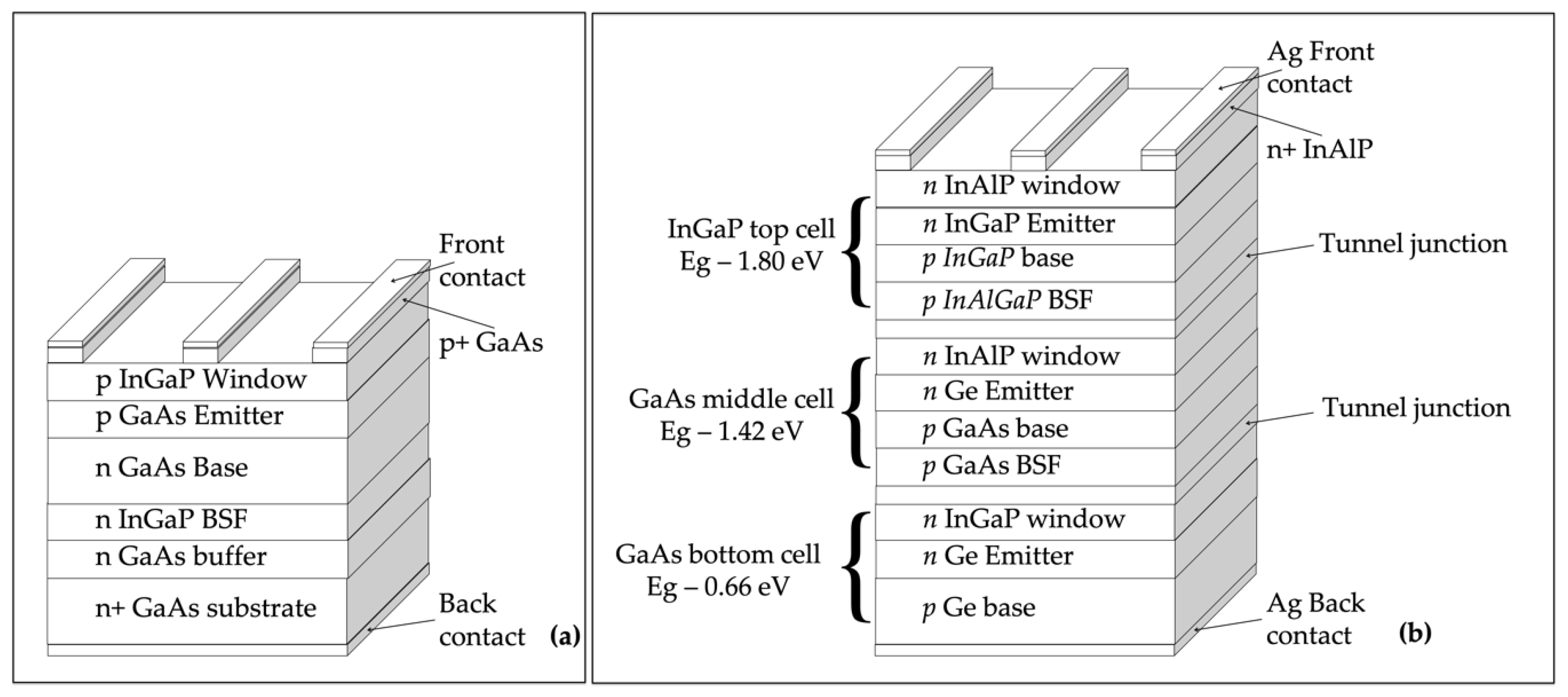
2.2. Gallium Arsenide (GaAs)

In the second part of the last century, in parallel with silicon technology, other materials capable of producing sophisticated devices including high-efficiency solar cells, were studied. In particular, in 1954 Welker published a first work showing the behavior of a GaAs “photocell” as a function of illumination intensity. In 1955, Gremmelmaier [17] reported the characteristics of two polycrystalline GaAs solar cells, which had measured efficiencies of 1% and 4% while illuminated with “sea-level sunlight”. Gremmelmaier expected a higher efficiency if monocrystalline GaAs was used. This material shows some intrinsic advantages with respect to silicon, such as a direct energy gap whose value is well-suited to sunlight and better withstands bombardment by ionizing radiation, making it suitable for space use. Unfortunately, GaAs is particularly sensitive to structural defects and its performance strongly depends on the intrinsic quality of the single crystal. It was necessary to wait 10 years in order to develop epitaxial growth techniques that were able to produce a small solar cell showing an efficiency of 13% [18], which is quite low compared to the theoretical efficiency of 26% [19]. It was already known [20] that the direct recombination process, occurring in poor-quality GaAs crystals, limits the cell output. Moreover, it was shown that a high surface recombination velocity was the most probable origin of the poor performance practically obtained for GaAs cells [21]. A heteroface cell, consisting of a p-type Gal-xAlxAs or InGaP layers on a p/n GaAs cell (Figure 2a) represented the keystone to overcoming the problems related to interface states [22,23]. The great boost due to the strong demand for space cells to be installed in the ever-increasing number of telecommunications satellites meant that the GaAs technology could reach the production of 5000 cells per week with an area of 2 cm × 4 cm. This was made possible because the technology passed from the liquid phase epitaxy (LPE), developed in the 1970s in the Hughes Research Lab (HRL), to the metal organic chemical vapor deposition (MOCVD) technology developed in the 1980s by Applied Solar Energy Corp. (ASEC). The key points of this technology were [24,25]:
  • Monocrystalline Ge substrate that, in addition to allowing an epitaxial growth of GaAs, provides a p/n junction sensitive to infrared light;
  • Epitaxial GaAs layer, thin enough to allow infrared light to reach the junction with Ge, grown by MOCVD process;
  • Upper AlGaAs layer with the primary function of eliminating surface defects and acting as a window layer for the cell;
  • Antireflecting bi-layer (SiO2 + Al2O3) coating with the double function of minimizing the sunlight reflection and preventing any damage to the underneath AlGaAs layer due to humidity;
  • Interdigitated metal (Ti–Pd–Ag) external contacts. In order to avoid any possible diffusion of metal atoms into the active layers, a capping p+ GaAs coating was deposited between AlGaAs and the contacts.
In the 1990s, dual-junction solar cells based on Ge/GaAs/AlGaAs system showed an efficiency, under extraterrestrial condition, of about 20%. In this period, many satellites were supplied with GaAs-based solar modules. GaAs panels with an efficiency over 20% represent an attractive choice for low-earth orbit (LEO) satellites [26], where the aerodynamic drag represents a problem, it is mandatory to use panels that are as small as possible; moreover, transport in orbit with a launch vehicle requires objects that are as light as possible. These considerations confirm that GaAs-based technology is widely accepted for space application. Furthermore, the MOCVD growth technique showed that only a small additional growth time is needed for adding a top cell and a tunnel diode to a bottom GaAs cell, increasing the interest in cascade cells. The higher efficiency exhibited by these cells, although costlier on cell scale, lead to a considerable reduction in the weight and costs of the whole system, making them even more attractive for space uses. On the contrary, the only way to exploit this technology for terrestrial use is to couple solar cells with light concentration systems making up for the higher cost of the system with less use of the material [27,28].
Nowadays, triple junction (3-J) GaAs-based solar cells (Figure 2b) under a concentration of 508 (508 times the irradiance of 1 sun) show an efficiency of 46% over a designed area of 0.05 cm2. Four junctions (4-J) minimodule (10 cells) under 230 suns exhibit an efficiency of 41.4% over an aperture area of 121.8 cm2. Multijunctions (nGaP/GaAs/InGaAs) for space use show an efficiency of the order of 31.2% under AM 1.5 [3]. At the same time, since the end of the 1970s, GaAs thin-film solar cells technology was developed [29], demonstrating its competitiveness both in terms of long-term stability and reasonable cost [30], reaching an efficiency of 29.1% (aperture area of 0.998 cm2) in recent years [3]. The main process adopted for the realization of the GaAs thin layer consists of the epitaxial lift-off (ELO) method to separate the GaAs film from the substrate. Production costs are appreciably reduced by re-using the substrate [31,32,33].

2.3. Copper Sulfide (Cu2S)

Thin film technology wasn’t implemented only for crystalline epitaxial growth. Materials with good photovoltaic responses both in amorphous and polycrystalline form have been studied since 1954, when Reynolds published a first work on the CdS/Cu2S heterojunction (Figure 3a) [1,2]. This first polycrystalline thin-film solar cell raised many expectations when, around the 1980s, a 10% photovoltaic conversion efficiency was achieved using ZnCdS as a window material coupled with Cu2S [34]. By replacing CdS with ZnCdS, the interface states introduced by the lattice mismatch between CdS and Cu2S were almost completely removed. However, this cell did not have the success that the pioneers expected due to over-time instability problems. Briefly, Cu2S is not a stable material when subjected to the electric field of the p/n junction; in fact, it frees Cu atoms, which form metallic filaments that channel the reverse current, causing the destruction of the junction barrier [35]. For this reason, this system was slowly abandoned, and the researchers began to take an interest in two other excellent photovoltaic materials: CdTe and CuInSe2.

2.4. Hydrogenated Amorphous Silicon (a-Si:H)

In 1975, within extensive research on amorphous semiconductors, it was unexpectedly discovered that the a-Si:H alloy can be doped with substitutional impurities such as boron (p-type) and phosphorus (n-type) [36]. Immediately after this, a solar cell exhibiting a 2.4% efficiency was realized [37]. The intrinsic disorder of the amorphous phase is effective in a lot of defects, which limit the mobility and the mean lifetime, contributing to the recombination of the photogenerated carriers. For this reason, a less defective intrinsic material (i: a-Si) was used as an absorber layer. In the following years, a-Si:H-based solar cells were produced both in substrate or in superstrate configuration, which means a p-i-n or n-i-p system, respectively. It became clear that the final productivity of the cell was strongly influenced by a consistent degradation of its PV parameters as a consequence of the light exposure (Light Induced Degradation (LID)), which creates metastable states in the energy gap. The recombination of photogenerated electron–hole pairs releases enough energy to break a weak bond, producing a pair of dangling-bond defects. To prevent the recombination of the two neighboring broken bonds a hydrogen atom moves from an adjacent Si–H bond. Annealing at temperatures of about 150 °C for one hour restores the original condition, allowing the hydrogen atoms to return to their original positions. In other words, the absence of a long-range order and the presence of dangling bonds produce states in the energy gap that prevent charge carriers to move freely [38,39]. Subsequent studies have clarified that this behavior was due in part to the large number of defects generated from the amorphous nature of the material and partly caused by interfaces; a-Si is usually grown by a plasma-enhanced chemical vapor deposition process (PECVD) in which silane is dissociated into an RF plasma [40]. The final quality of the material is determined by plasma chemistry and growth kinetics, which is highly influenced by temperature. In order to improve the film quality, the p-i-n stack was deposited at a temperature just below the amorphous-to-microcrystalline transition; to improve the interface quality, a tandem junction was realized, bringing together an a-Si:H top and microcrystalline µc-Si:H bottom cell (micromorph-cell). In this tandem cell, the different values of the energy gap of a-Si:H (1.7 eV) and µc-Si:H (1.1 eV) allows the exploitation of a wider region of the solar spectrum [41]. Starting from 1990, a new system based on three subcells integrated in a single device (triple junction) was considered, in order to improve the collection of the photogenerated carriers. The triple junction (3-J) was realized in an n-i-p sequence in which the topmost subcell exploits a typical a-Si:H-based sequence, while the middle and the bottom subcells were based on an a-Si–Ge:H alloy [42]. The Ge content was controlled in order to obtain an energy gap width of 1.6 and 1.4 eV for the middle and the bottom subcells respectively. 3-J devices (Figure 3b), realized on laboratory scale, exhibited an initial active-area efficiency of 14.6%, corresponding to a stabilized total-area efficiency of 12.1%, very similar to the best performance of micromorph tandem cells. For these solar cells, initial and stabilized, are significant for their performance before and after light-induced degradation, respectively.
The modest performance of these cells caused many market losses. This technology covered only 0.3% of the annual photovoltaic production in 2017.

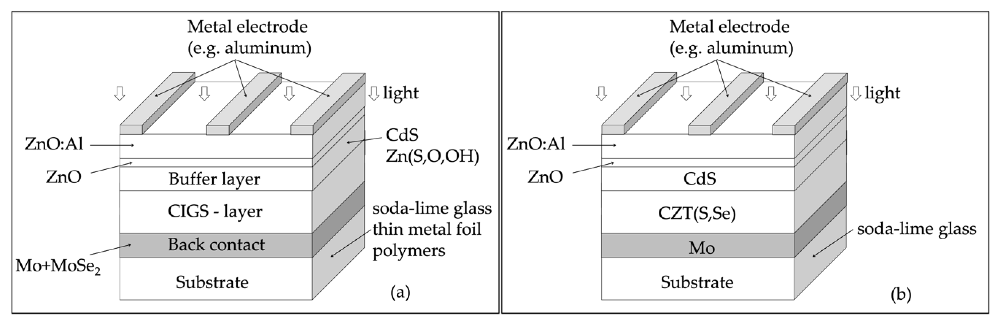
2.5. Copper Indium Gallium Diselenide (CuInGaSe2)

The development of CuInSe2 (CIS) solar cells started in the early 1970s, when a 12% efficient solar cell based on a p-type CIS single crystal coupled with a n-type CdS thin film was realized [43]. Only few years later, the first entirely thin- film solar cell based on CIS/CdS exhibiting a 5.7% efficiency was realized [44]. Many efforts were made in order to improve the photovoltaic performance of this solar cell, involving several laboratories and researchers, but it took more than 30–40 years to realize CIS-based thin film solar cells that were efficient enough to compete with the most studied silicon-based ones. During these years, some important modifications were introduced in stoichiometry and in the growth process of the CIS film in order to completely exploit its potential. In particular, Ga was added to form CuInxGa(1−x)Se2 (CIGS), whose energy band gap can be adjusted by the percentage of Ga incorporation [45]. By exploiting the higher band gap of the quaternary compound, the photovoltage (Voc) increased and a reduced recombination in the conduction band of CdS was observed. All this work led to a 17.7% efficiency solar cell in 1996 [46]. MgF2 antireflecting coating and a ZnO window layer helped to improve the photocurrent (Isc), resulting in an 18.8% efficient device [47]. By gradually changing the Ga and In concentration inside the CIGS layer, a band gap grading was obtained. The interface with CdS was formed with a very thin CIGS layer with a higher Ga concentration, resulting in an increased built-in potential, which means an enhanced photovoltage (Voc). By raising the In concentration in the remaining CIGS material, the energy band gap was lowered; as a consequence, the Isc increased. This engineered band gap profile attained a larger diffusion length in the minority carriers and reduced recombination in the space-charge region, leading to a 19.2% efficient ZnO/CdS/CIGS solar cell in 2003 [48]. The energy band gap profile was definitively stressed when, approaching the back contact, the Ga concentration was increased inside the CIGS layer. Consequently, a larger energy gap in the back-contact region was realized and a mirror for the minority carriers was obtained, increasing their diffusion length [49,50]. In this favorable condition, a 19.9% efficient solar cell was realized in 2008 [51]. In 2010, an efficiency of 20.3% was reached [52], definitively overcoming the 20% psychological barrier. Three years later, the Swiss Federal Laboratories for Materials Science and Technology (EMPA) obtained a 20.4 efficiency GIGS-based solar cell on a flexible polymeric substrate (Figure 4a) [53]. This impressive result opened the route to the roll-to-roll continuous production of completely flexible PV modules.
In the same year, substituting the CdS buffer with a more environmental sustainable Zn(O, S) layer and improving the CIGS film by using potassium doping, an efficiency of 20.8% was reached [54]. The efficiency became 21.7% [55] by optimizing the alkali post-deposition treatment of the cell. Recently, a CIGS-based solar cell world record efficiency of 23.35% was achieved by Solar Frontier [56] over a designated area of about 1 cm2. The use of Cu(In, Ga)(Se, S)2, together with a high-temperature heavy alkali (Cs) post-treatment of the absorber layer, results in a reduced defect density. The enhanced quality of the Cu(In, Ga)(Se, S)2 allows the opportunity to benefit from the effects of a wider absorber bandgap. Consequently, the reverse saturation current density decreases, producing an important enhancement in photovoltage and fill factor (FF), leading to the world record efficiency result.
Today, CIGS technology, with an annual production of around 1.8 GWp, covers a market share of 1.9%, which is principally supported by three producers: Miasolè, Solibro and Solar Frontier.
Within the past ten years, the photovoltaic world has realized that 20% efficiency is more than enough to guarantee the so-called grid parity, or to make photovoltaics widely competitive with traditional energy sources [57,58,59]. To significantly affect the world energy market, the production volume of photovoltaic modules must be a few terawatts/year (TW/yr). TW-scale production implies a correct availability of the constituent elements. For CIGS technology, the greatest risk is represented by the availability of indium (In), since it is even more widely used in expensive devices such as flat panel displays (FPD) [60,61]. In this condition, the estimates predict that the demand for In will exceed the supply, when CIGS manufacturing volumes will reach 100 GW/yr. From this point of view, it is mandatory to exploit other materials, whose constituents are more available on the earth crust. For example, we have to consider that the abundance of Cu, Zn, Sn, and Sulphur is 68, 79, 2.2, and 420 ppm respectively, which is considerably higher compared to that of In, Cd, Te of 0.16, 0.15, and 0.001 ppm, respectively.

2.6. Cu2ZnSn(S, Se)4—(CZTSSe)

Ternary and quaternary chalcopyrites (CuInSe2 and Cu(In, Ga)Se2) represent a promising solution, but the increase in the prices of rare metals (In and Ga) heavily influences the cost–efficiency ratio.
Another opportunity is offered by replacing rare metals with cheap and widespread zinc and tin, and different new materials are considered for replacing CIGS and CdTe. Among them, one of the kesterite family, namely Cu2ZnSn(S, Se)4 (CZTSSe), has become intriguing as an alternative absorber in thin film solar cells. CZTSSe exhibits a native p-type conductivity, high optical absorption coefficient (>104 cm−1 in the visible part of the solar spectrum) and tunable direct band gap in the (1.0/1.5) eV range, depending on the S and Se concentration [62,63,64].
In 1996, the first CZTS-based cell exhibiting an efficiency of 0.66% was realized [65]. In the following decades, the knowledge of the material improved and, as a consequence, the performance of the solar cell increased too, reaching an efficiency of 12.6% in 2013 [66]. Different physical and chemical techniques are used for the deposition of the CZTSSe layer. Among them, the most common are: RF sputtering with post-deposition treatment in S and/or Se atmosphere at high temperature (>di 500 °C), thermal evaporation, pulsed laser deposition, spray pyrolysis, spin coating, sol-gel. The best performing cell has been obtained by IBM, making use of a simple nanoparticle ink-based process. All these different manufacturing methods indicate a cost-effective approach for this technology, but they are not effective in terms of the finished device’s performance. In fact, it was clear from the beginning that one of the main problems affecting this material is the possibility of generating many stoichiometric defects during growth both in bulk material and in the form of thin film. The similar ionic radii of Cu and Zn promote the formation of CuZn and ZnCu antisites, which are characterized by having the lowest energy among the acceptor and donor defects. Given the high concentration of these native defects, compensation is offered through the formation of antisite pairs [ Cu Zn +   Zn Cu + ] distinguished by a very small formation energy. This cations disorder into the kesterite crystal lattice could be the reason for a poor performance, showing a reduction in the photovoltage and fill factor. Recently, improvements in open circuit voltage have been obtained by reducing the number of antisite defects via cation substitution with Cd, Mn, Ba, Fe, Ni and Co, demonstrating that a better control of stoichiometry is needed for obtaining high efficiencies [67]. Moreover, the most efficient CZTSSe-based devices are processed by reacting precursors at atmospheric pressure; these methods are effective in reducing the re-evaporation of high-vapor pressure compounds, such as SnSe, Cu2SnSe3, Zn, Se and S, and in providing good control of the CZTSSe stoichiometry. This solar cell was born with the purpose of replacing the more expensive and less sustainable CIGS and, although they have a lot in common (Figure 4b), they are still far from the remarkable performance of CIGS-based cells. One possible explanation consists in considering the different role of the grain boundaries (GB) inside CIGS and CZTSSe. Some studies have recognized GBs as the origin of the extraordinary performance of CIGS. In this material, crystal defects and impurities present at GBs act as traps for majority carriers (holes for p-type CIGS), generating a depletion region [68,69,70]. The resulting electrostatic barrier repels holes from the GBs, assists electrons in reaching the n-type layers, enhancing the charge carrier collection, and prevents the recombination of the photogenerated electron-hole pairs. On the contrary, GBs in CZTS polycrystalline films act as recombination center for the electron–holes pairs and, to date, an effective method for their passivation has not yet been found.
The history of the development of the champion module efficiencies for silicon and thin-film technologies is depicted in Figure 5, together with their manufacturer, while the current performances are shown in Table 1.

3. CdTe-Based Technology

In the previous paragraph we presented the world of inorganic PV, except for the CdTe system. In the following, we will extensively describe the CdTe-based solar cell and modules, departing from the research which started in the 1960s and moving on to the technological aspects inherent in the module production.
CdTe is considered as a very good material to serve as an absorber in solar cells, due to its direct energy gap (1.45 eV), which is nearly ideal for photovoltaic energy conversion, corresponding to the maximum of the solar spectrum. Its high optical absorption coefficient allows the incident light, with energy above its band-gap, to be totally absorbed within 1 µm from the surface. A CdTe-based solar cell could exhibit a photocurrent of 30.5 mA/cm2 when illuminated with 100 mW/cm2 sunlight, offering a theoretical maximum efficiency close to 30%. Historically, the best performances were typically obtained with heterojunction in which the n-type partner was cadmium sulfide (CdS). Some different attempts were tried when p-type CdTe single crystals were coupled with In2O3 [71], ZnO [72] or a very thin n-type CdTe layer [73], obtaining a 13.8% maximum efficiency. The success of this material was not obtained by means of single crystal but, on the contrary, by exploiting one of its best characteristics, namely the possibility to produce a complete solar cell by simply using thin-film technology. In fact, CdTe/CdS total thin film heterojunction led to a 6% efficiency solar cell and this result has been known since 1972 [74]. However, the psychological limit of 10% efficiency was overcome in the 1980s only after a heat treatment in chlorine atmosphere was applied to the CdTe/CdS stacked layers [75]. In the following ten years, devices with efficiency close to 17% were made by optimizing both the front and the back contacts [76,77]. This was followed by a period of stasis in photovoltaic performance, in part due to intrinsic difficulties, such as the impossibility of extrinsically doping polycrystalline CdTe thin films and partly due to the fact that many researchers have devoted their activities to the technological transfer of production processes from laboratory to industrial scale.
Around 2010, the photovoltaic conversion efficiency began to increase again, reaching values close to 20% in a short time. The continuous increase in efficiency is largely due to the optimization of the layers making up the antireflecting coating (ARC), the transparent electrical contact and the window layer, as well as a careful choice of the glass substrate. This led to a substantial increase in the photocurrent, going from 26.1 mA/cm2 for a cell with 17.6% efficiency [77] to a 28.59 mA/cm2 photocurrent for a cell with 19.6% efficiency, corresponding to a rather modest increase in photovoltage [3]. Unfortunately, there aren’t any details in the literature concerning these remarkable results. However, it seems clear that the photocurrent increase is not only due to a very good optimization of the light harvesting, but also to an accurate management of the CdTe energy gap in order to extent the absorption to longer wavelengths. CdTe(1−x)(S, Se)x alloys show energy bandgap values smaller than CdTe when x ≤ 0.05, corresponding to a maximum increase in the cutoff wavelength of about 15 nm. The corresponding increase in photocurrent can be evaluated in 1 mA/cm2. Moreover, the use of a CdTe(1−x)(S, Se)x mixed compound reduces the lattice mismatch at the metallurgical junction, resulting in enhanced charge transport properties. In 2015, a solar cell based on a CdTe(1−x)(S, Se)x thin film exhibited a world efficiency record of (22.1 ± 0.5)%, showing the following parameters measured under the global AM 1.5 spectrum (1000 W/m2) at 25 °C: Voc = 0.8872 V, Isc = 31.69 mA/cm2, fill factor = 0.785 over a designated illumination area of 0.4798 cm2 [3,78].
The fabrication process of this solar cell is particularly suitable to be implemented in a large area, fully automated, in-line production. This is made possible by the electrical in-series integration of the cells directly inside the production process (monolithically integrated) by means of a robotic laser scribing. This technology realized a 11% efficient module in 2002 by depositing the CdTe thin film with the electrodeposition technique [79]. In the years 2010–2011, the number of factories able to produce tens of megawatts/years of CdTe modules were 10 units worldwide. The production was based on the close-spaced vapor transport (CSVT) or close-spaced sublimation (CSS) techniques for the deposition of the CdTe layer and an average module efficiency ranging from 10% to 12% was announced [80]. At the end of 2012 a 14.4% efficient device was reported, which became 16.1% at the beginning of 2013. In March 2014, a 17.5% efficient module was obtained, followed by a world efficiency record of (18.6 ± 0.5)% in 2015. The photovoltaic parameters of such a module, taken under the global AM 1.5 spectrum (1000 W/m2) at a cell temperature of 25 °C, are: Voc = 110.6 V, Isc = 1.533 A and fill factor = 0.742 over a designated illumination area of 7038 cm2 [3]. Commercial modules with an efficiency of 18.2% are now available on the market [81].
The first Solar, with a 2.4 GWp annual production, covers 2.3% of the market share.

3.1. The Solar Cell

A CdTe-based solar cell is typically realized with very thin stacked layers, arranged in such a way as to form a high-quality heterojunction. When CSS or CSVT techniques are used, CdTe thin films naturally grow as p-type, and are forced to select a n-type partner to make the p-n junction. The architecture of the heterojunction allows sunlight to pass through the n-type layer to reach CdTe where photogeneration takes place. To date, the best-found configuration is the CdS/CdTe system, where CdS is the “window”, while CdTe is the “absorber”. For this reason, the thickness of CdS film is never more than 100 nm to ensure excellent transparency. The free carrier concentration of both the window and absorber films ensures that the electric field mostly falls into the absorber material, so that all the photogenerated electron–hole pairs can be separated and pushed towards the external electrical contacts. These auxiliary layers complete the device, ensuring the passage of the photocurrent. High-efficiency CdS/CdTe solar cells are produced in a superstrate configuration, which means light passes through the substrate and the front contact is as transparent and conductive as possible. Instead, the back-contact, which is generally opaque, has to ensure the ohmicity with p-type CdTe in order to efficiently harvest all the photocurrents (Figure 6a).
In substrate configuration, the manufacturing sequence starts with the back contact, followed by the CdTe/CdS films, ending with the transparent electrical contact (Figure 6b). This configuration is particularly intriguing since it allows devices to be made on opaque substrates such as metal and polymeric foils, opening a means for the production of flexible, light and cost-effective modules. Moreover, flexible substrates enable the roll-to-roll technique, which is very suited for vehicle- and building-integrated photovoltaics (VIPV and BIPV). It is undeniable that this architecture could overcome one of the problems of superstrate configuration; in fact, CdTe doping and CdTe/CdS junction formation are separated production steps, which could be individually optimized. On the contrary, one of the unsolved issues is the formation of an ohmic back-contact, which is partly resolved by the introduction of a buffer layer between the metallic part of the contact and the CdTe surface. By using Te/MoO3 and CuxTe as buffer layers, coupled with a Mo metal contact, solar cells exhibiting efficiencies in the range (13.6/11.3)% are obtained [82,83]. Furthermore, individual cells, monolithically integrated inside a module, require the electrical insulation of the metal substrate from the back-contact, otherwise series interconnection would not be possible, as the system has a common electrode. This dielectric film also acts as a barrier against the diffusion of metal atoms from the substrate into the absorber layer and, consequently, to the junction region. Al2O3 or SiO2 films, 100 nm thick, directly sputtered onto the metallic substrate, are excellent buffer layers from both these points of view.
The final behavior of the CdTe-based solar cell strongly depends on the interaction among the constituent layers, which depend on the deposition order, highlighting that the layer sequence is crucial. CdTe/CdS solar cells realized in substrate configuration are younger compared with the superstrate ones, and a lot of research on the layer interaction, diffusion, interfaces, back-contact and doping issue should be done.
We are principally interested in superstrate configuration, since the best performances are obtained by solar cells fabricated following this arrangement.
Briefly summarizing, the main steps of the production process are: (i) to deposit cadmium and tellurium as inexpensively as possible, (ii) to activate the system in chlorine environment at high temperature, (iii) to couple a window layer to the absorber layer to form an efficient heterojunction. The other production steps are typical of thin-film technology such as the choice of the electrical contacts, whose principal requirements are to be as conductive as possible and to be transparent to sunlight in case of the front contact. Since we are dealing with superstrate configuration, the substrate must be chosen to ensure maximum light transparency for the whole useful life of the solar cell.
Now, we will review each of the production steps and the main requirements the individual materials should have.

3.1.1. The Substrate

Rigid glass is normally used in the superstrate production of high-efficiency cells and modules. Since solar light passes through the substrate, glass has to be as transparent as possible in order to minimize parasitic light absorption. The most common commercial glasses are generally known as “soda-lime glass” (SLG). Silica (SiO2) is the principal component of this type of glass (up to 75%/76%), making it particularly resistant to thermal shocks, but its high melting point and its viscosity make processing difficult. To simplify the manufacturing process, other substances are added. One is “soda”, or sodium oxide (Na2O) (14%), for lowering the glass transition temperature. Nevertheless, soda makes glass unwantedly water-soluble and, in order to provide a better chemical stability, “lime” or calcium oxide (CaO) is also added (9%). In addition, magnesium oxide (MgO) and alumina (Al2O3), contribute to durability (see Table 2). Inexpensive minerals such as trona, sand, and feldspar are typically used in place of pure chemicals, making soda lime glass really cost-effective. Unfortunately, when starting with minerals, some impurities, such as Fe2O3 and MnO2, which are responsible for a transparency decrease in the visible part of the solar spectrum, are un-intentionally introduced. For this reason, iron-free glasses are normally used in CdTe technology, gaining 8% transparency at short wavelengths (λ < 300 nm) [84].
Some attempts to employ flexible substrates were made by using polymers, such as the Dupont’s polyimide, which permits a high-rate roll-to-roll technology in order to produce large-area, very light photovoltaic devices at reasonably low costs. The optical transparency of standard SLG and polyimide are comparable at long wavelengths, but below 530 nm polyimide transmittance is not enough for PV application, despite thin foils being used (Figure 7a). This turns into a photocurrent loss of at least 3 mA/cm2. For this reason, together with the temperature limitation, solar cells realized with this polymer never exhibit an efficiency over 13.8% [85].

3.1.2. The Transparent Electrode

In thin-film photovoltaic technology, one of the most severe requirements is the use of transparent and conductive electrodes, capable of letting light pass through, which must reach the underlying active layers and must be electrically conductive in order to efficiently collect the photogenerated carriers without introducing unnecessary series resistances. Transparent and conductive oxides (TCO) are high-performing, exhibiting transparencies close to 90% in the wavelength range of the visible light and electrical conductivity up to 104 Ω−1·cm−1. A high electrical conductivity and high transparency to visible light seem to be contradictory. In fact, these requirements need opposite properties in terms of band gap, which must be:
  • Large enough to avoid optical absorption;
  • Small enough to allow the filling of the conduction band by a near-free electron at the working temperature.
Concerning the optical transparency, the low-energy limit is set by the width of the energy band gap. On the other hand, the electrical conductivity needs heavy doping, which often means a degenerate condition characterized by the Fermi level inside the conduction band. In this condition, the energy gap, evidenced by the absorption of light, is wider when compared with the fundamental one, according to the Burstein–Moss effect [86].
The most common TCOs used in CdTe technology, are: Sn-doped In2O3 (ITO), F-doped SnO2 (FTO), Al-doped ZnO (AZO) and Cd2SnO4 (CTO). These TCOs are near-degenerate semiconductors, but only ITO exhibits a typical free-carrier absorption in the near-infrared (NIR) region of the solar spectrum. This drawback, together with the indium scarcity [87], mean ITO is not widely used in PV industrial production. All these TCOs are coupled with high-resistivity transparent oxide buffer layers (HRT’s) with the aim of reducing shunt effects coming from pinholes in active layers hindering the diffusion of impurities from TCOs or from the substrate. The transmittance of some of these TCO is reported in Figure 7b. On laboratory scale, un-doped SnO2, In2O3 and ZnO are HRT layers commonly coupled with ITO, while FTO is generally paired with pure SnO2 and CTO is combined with Zn2SnO4 (ZTO) [88]. The typical bilayer structure of these TCOs change the chemical and physical interaction between the front contact and the window layer, as is seen when ZnO and CdS, brought at high temperature, form an intermixing layer, which modifies the optical properties of both films.

3.1.3. The Window Layer

The most used n-type partner with CdTe is cadmium sulfide (CdS), which exhibits n-type conduction due to stoichiometry defects, such as sulfur vacancies, which are formed during the film growth. With an energy gap of 2.42 eV, it allows sunlight to pass up to a wavelength of 512 nm, inhibiting the passage of the near ultraviolet light to which SLG substrate and TCO layers are still transparent. Moreover, self-doping is effective in obtaining resistivity of the order of (106/107) Ω·cm, the same order of magnitude as was obtained with CdTe films. A golden rule for the formation of a p/n junction in efficient solar cell is that the electric field falls principally into the p-type region (CdTe). As the mobility of electrons in CdS is significantly greater than the mobility of holes in CdTe, this requirement is satisfied only if the density (p) of the p-type carriers in CdTe is appreciably less than the density (n) of the n-type carriers in CdS. In dark conditions, this rule is not satisfied, but under light, where the solar cell works, the photoconductivity of CdS helps to distribute the electric field into the CdTe film. Concerning the transparency of the wavelengths of sunlight, which are shorter than the gap cutoff, since nothing can be done about the absorption coefficient (α), it is only possible to work on the optical density (α·d) by using extremely thin films, allowing the passage of light despite the high value of the absorption coefficient (t < d, t ≤ 100 nm, where d is the average absorption length and t is the film thickness).
In order to better exploit the visible spectrum of sunlight, window materials with a wider energy band gap were studied. The ZnCdS system, varying the energy band gap from 2.42 (CdS) up to 3.6 eV (ZnS), seemed a good candidate. The expected increase in the photovoltaic parameters (Voc and Isc) of the ZnCdS/CdTe solar cells did not take place [89]. The most reliable explanation is that interface defects have increased because the Zn–Cd–S–Te system is not as favorable as the Cd–S–Te one in reducing the structural defects responsible for the recombination of the photogenerated carriers. In fact, it is now accepted by many researchers that CdS is crucial for obtaining solar cells with excellent performances, despite the high lattice mismatch with CdTe (≈10%). This drawback is overcome since the high temperature deposition of CdTe guarantees a strong interaction between the two materials. As a consequence, an intermixed layer is formed, minimizing the lattice mismatch and the interface states resulting from structural defects.
Since the quality of the solar cell strongly depends on the interaction between the active layers, the deposition techniques used for the film growth play an essential role. The techniques generally used for the deposition of both the active layers can be divided into low (L-T) and high temperature (H-T).
CdS is normally deposited at a substrate temperature below (L-T) or above (H-T) 200 °C. RF sputtering, chemical bath deposition (CBD) and high vacuum thermal evaporation (HVTE) belong to L-T processes, while close-spaced sublimation (CSS) and close-spaced vapor transport (CSVT) are H-T deposition procedures.
The CBD process gives high-quality CdS films characterized by a very high density and compactness which are pin-hole free, but as-deposited films are not suitable for the formation of an efficient junction when coupled with CdTe [90,91]. A heat-treatment at 400 °C is needed to remove the Cd and S excesses naturally present in the L-T deposited films. This treatment is also effective in changing the crystalline structure from a hexagonal-cubic mixed phase to a more stable unique wurtzite phase.
On a laboratory scale, this method offers excellent results, but in industrial production sputtering and H-T processes are generally preferred since CBD is a low-speed process and it produces a large amount of waste, which must be expensively recycled.
CdS films can be sublimated at temperatures above 700 °C in a high-vacuum chamber and deposited on a substrate held at a temperature below 200 °C. As in the case of the CBD deposition, an annealing at a temperature of 400 °C, under vacuum or in a hydrogen atmosphere, is needed to remove stoichiometry defects and to obtain the necessary chemical stability. Unfortunately, CdS films deposited with this technique have low compactness with a high density of pinholes.
For this reason, very thick CdS layers (≈300 nm) must be used to produce efficient solar cells, but with unavoidable photocurrent loss due to poor light collection.
The HVTE technique is used for producing flexible PV modules, where a thin polymeric foil is used as a substrate, which can withstand temperatures up to 400 °C [92].
Sputtering is considered an L-T deposition technique even though the surface of the growing film is constantly bombarded by electrons and impinging atoms, which exchange their kinetic energy and promote typical high-temperature effects. In fact, the RF sputtering deposition is not suitable to produce CdS films with the proper quality and chemical stability to be used in CdTe-based solar cells. Only reactive RF sputtering, introducing oxidizing atoms into the process chamber, such as fluorine- or oxygen-containing gases, produce high-quality CdS films which are able to form a good CdS/CdTe heterojunction. What happens in the sputtering discharge when a hydrofluorocarbon or oxygen gas is introduced to the process gas (Ar) is well known: the glow discharge ionizes the decomposed elements of the reactive gas, producing free fluorine or oxygen ions [93]. Some of these, being electronegative, become negative ions and, as a consequence, they hit the surface of the growing film, which could be considered the positive electrode for the main part of the RF period. These ions have sufficient energy to sputter-back the weakly bonded Cd and S atoms on the surface of the CdS film. As a result, a stoichiometric, dense and better-crystallized film is obtained with a great improvement in optical and structural quality. Moreover, fluorine or oxygen ions could react with CdS, forming CdF2 or CdSO3, respectively. These are excellent dielectric insulating materials, principally segregated into the grain boundaries of the polycrystalline CdS film, contributing to their passivation. The same segregation on the surface of the growing CdS film may adjust the interaction with CdTe during its high-temperature deposition (Figure 8b). Among the H-T deposition technique, CSS is the most popular and CdS films obtained with this process exhibit superior qualities, even though depositions carried out in pure Ar provide low-density films with many pinholes. If oxygen is added into the process chamber, the deposition equilibrium is substantially altered and the growth slows down, since the grain boundaries of the growing film are decorated with oxides (CdSO4, CdSO3) [94]. As a consequence, a denser film without pinholes is easily obtained. In this case, the CdS surface is covered by a mixed CdSO4-CdSO3 thin layer. High-efficiency solar cells are obtained when, CdS films deposited with CSS in Ar + O2 process gases, are annealed in an H2 atmosphere (Figure 8a).

3.1.4. The Absorber Layer

Homojunction, heterojunction, p-i-n and Schottky barrier have been historically investigated for CdTe-based solar cell production [95,96,97]. It was immediately clear that heterojunction is the most efficient structure, probably due to the intermixing layer formed during CdTe deposition or during post-deposition heat-treatments. This layer, removing the structural native defects, makes the window/absorber interface very close to a homojunction exhibiting an ideality factor close to unity. This homojunction-like behavior characterizes the high-efficiency CdTe polycrystalline thin-film solar cells, confirming that the recombination centers are far away from the junction, i.e., the depletion layer is virtually free of interface states.
Typically, L-T and H-T deposition technologies are both widely used to produce CdTe thin films.
The highest efficient devices are generally obtained by H-T processes, in particular CSS (Figure 9) and CSVT, which are industrially implemented for the production of commercially available 18% efficiency CdTe-based modules. Due to the high deposition temperature, the polycrystalline films are characterized by large, columnar and slightly defective grains with an average dimension in the range of (5/10) µm for film thickness of about (6/8) µm. These techniques allow high growth rates (up to some µm/min) at the expense of a homogeneous growth of the crystalline grains. As an immediate consequence, wide grains, with a lot of pinholes in the middle, are routinely obtained although, the film thickness is already very large.
In this form, it is very hard to extrinsically dope CdTe, because any attempt carried out to date has highlighted the tendency of p-type dopants to segregate into the grain boundaries, generating short-circuit paths that kill the junction. With only the intrinsic doping, due to stoichiometric native defects, the typical dark p-type conductivity, shown by CSS-deposited CdTe films, is of the order of (10−4/10−5) Ω−1·cm−1. By considering the absorption coefficient, the visible light penetrates into the CdTe layer up to 1 µm. Due to photo-generation, this part becomes more conductive (10−2 Ω−1·cm−1), while the rest of the film, persisting in dark conditions, cannot change its electrical conductivity. This corresponds to a series resistance which afflicts the device, inhibiting the complete collection of the photocurrent.
From this point of view, it is mandatory to reduce the thickness of the CdTe layer, since a thickness of around 2 µm is more than enough to absorb all the visible light, considering that CdTe exhibits an absorption coefficient in the range of (104/105) cm−1. This thickness is optimal both for optical and electrical requirements, even though it’s very difficult to obtain CSS-deposited pinhole-free films with the requested quality and compactness.
In order to avoid these two unpleasant drawbacks, oxygen is generally added to the inert gas in the CSS or CSVT process chamber. Due to the presence of CdO and TeO2 species, an increased surface diffusion of the incoming Cd and Te atoms is expected; as a consequence, a less defective CdSTe layer could be formed. The presence of oxygen affects the nucleation process, increasing the number of nucleation sites and promoting a denser growth of the CdTe film. In these conditions, a small amount of CdTeO3 is formed, performing an appreciated passivation effect of the grain boundaries [98].
A similar result is obtained if oxygen is added to the Ar process gas during the CdTe sputtering deposition by using a ceramic target. In both cases, a reduction in the grain size is clearly evidenced and a deep profiling analysis, made by secondary ion mass spectroscopy (SIMS), put in evidence a Te-rich surface concerning the CSS-film, while the sputtered CdTe layer shows a Cd-rich stoichiometry on the surface [99]. The sputtered film exhibits an n-type conductivity of about 10−3 Ω−1·cm−1. A sputtered thin film, deposited on top of a CSS-deposited one, is mainly segregated into the grain boundaries, filling in all the pinholes and giving rise to a p-n junction formed between the grain boundaries and the bulk. This beneficial passivation efficiently acts as a mirror for the minority carriers, increasing their lifetime and preventing shunt paths in the junction region.
In recent years, an attractive hypothesis about the optimization of the photovoltaic parameters of the CdS/CdTe solar cell has been considered. In particular, it is known that a solar cell under AM 1.5 G reaches maximum efficiency when the energy gap of the absorber layer is 1.34 eV [19,100]. From this point of view, the energy gap of CdTe is slightly wider, being 1.5 eV. Following this idea, First Solar improved the efficiency of the CdTe-based solar cells by using CdTe(1−x)Sex as an absorber material. In fact, by adjusting the stoichiometric composition x, a graded profile of the energy gap could be obtained. According to [101], when x ≈ 0.4, the energy gap of the CdTe0.6Se0.4 alloy is 1.4 eV and a better collection of the solar light extended to a longer wavelength compared to the pure CdTe is observed. An engineered profile of the energy gap could be effective in improving the photocurrent if a CdTe(1−x)Sex alloy is used in the front region, while maintaining the photovoltage in the bulk of the CdTe layer. Moreover, when a CdS/ CdTe(1−x)Sex heterojunction is made, it was found that the thickness of the CdS layer can be drastically reduced or the layer can be avoided, decreasing the parasitic absorption in the high-energy region of the solar spectrum, and obtaining an increasing photocurrent [102]. Additional improvements can be obtained if the CdS layer is replaced with MgZnO, a material with which CdTe and CdTe(1−x)Sex have a better alignment to the energy band. This material is characterized by a better transparency in the high-energy region with respect to CdS [103,104]. Furthermore, a greater passivation effect of the defects due to the presence of Se is effective for a longer lifetime of the charge carrier in CdTe(1−x)Sex compared to CdTe [105]. By adopting these measures, solar cells with an efficiency of over 22% were obtained, including the world record [3].
These excellent results are a consequence of more than 20 years of research focused on all the aspects that influence solar cell behavior, including materials, interfaces, deposition techniques, electrical contacts, substrates and last but not least, production techniques which must be intrinsically easy enough to scale up to the industrialization of large modules.
However, alternative ways to achieve high efficiency devices should not be overlooked . In fact, high-efficiency solar cells have also been made on flexible polymeric substrates, where the basic requirement is a low process temperature.
CdTe and CdS films, deposited by HVTE at a temperature of about 200 °C with a typical thickness of (2/3) µm, show very good smoothness and compactness with a characteristic grain size of (100/500) nm [106]. The dimension of crystallites suggests that the mobilities and lifetimes of the charge carriers are very low, and not suitable to form an efficient p-n junction capable of properly collecting the photogenerated carriers.
Never, as in this case, is a post-deposition treatment, the so-called “chlorine treatment” needed. This heat-treatment has the ability to reduce the stacking faults, misfit dislocations and grain boundaries, increasing, accordingly, the crystalline grain size [107]. By using commercial FTO-covered SLG substrates, all HVTE-deposited CdS/CdTe solar cells exhibit efficiencies of about 15%. The efficiency is lowered to 12% if a polyimide substrate is used [108].
Among the L-T techniques, the electrodeposition of semiconducting materials was originally presented in the 1970s [109,110]. Only in the early 1980s was an all thin-film electrodeposited CdTe-based solar cell developed, exhibiting a notable efficiency of 8% [90,111,112]. Recently, a record efficiency of 15.3% has been announced, exploiting a different device architecture. Normally, the electrodeposited CdTe layer exhibits an n-type conductivity. As a consequence, the active junction is shifted at the back-contact, which forms a Schottky barrier with CdTe. An innovative SLG/FTO/n-CdS/n-CdTe/p-CdTe/Au layer sequence was implemented for producing the record solar cell. The main improvement is represented by a buried-homojunction close to the back-contact. The presence of a p-type CdTe thin film at the back-contact allows for better control of the junction position inside the absorber layer, resulting in an enhanced barrier height and photogenerated carrier collection [113].
RF magnetron sputtering deposition is a simple technique for industrial coating needs after being scaled down to laboratory requirements. For this reason, the opposite path is considered obvious and sputtering technique is increasingly considered a key process when a high-density film with good adhesion to the substrate is requested [114]. When CdS and CdTe compounds are deposited, the electro-optical properties of the films strongly depend on the sputtering parameters as well as the sputtering power, Ar and reactive gas pressure, bias voltage, substrate temperature, target-to-substrate distance, etc. This great variety of process parameters allows a very fine-tuning of the physical characteristics of the growing film. Exploiting the excellent coverage and high density of the sputtering-deposited films, a 2 µm thick CdTe layer is used to realize very thin solar cells [115]. By suitably adjusting the chlorine treatment, CdTe thin films with crystalline grains large enough for achieving high-efficiency solar cells could be obtained. Following this philosophy, in the early 2000s a 14% efficient solar cell has been produced [116].

3.1.5. The Heat-Treatment

It is not important which technology is used to deposit the CdTe layer; whether it is LT or HT, the result obtained is always the same, i.e., very limited conversion efficiency. Evidently the as-deposited material does not have a suitable crystalline quality to obtain a good device, since it is characterized by a large number of structural defects, which hinder the motion of the charge carriers promoting the recombination of the photogenerated electron–hole pairs.
For this reason, in CdTe technology an annealing, at a temperature in the range (350/400) °C, in chlorine atmosphere, is currently used. This treatment is inspired by the monocrystalline vapor phase growth of II-VI compounds, in which the transport agent is a halogen gas, normally chlorine. Historically, chlorine is supplied by depositing a CdCl2 on the top of the CdTe film. A first attempt was made by vapor depositing a CdCl2 thin film or by drop-casting a Cl-salt/methanol solution followed by an air-anneal. At the treatment temperature, the surface of the CdTe film becomes mobile due to the vapor pressure, and the following process is normally assumed to occur
CdTe(s) + CdCl2(s) → 2Cd(g) + ½Te2(g) + Cl2(g) → CdCl2(g) + CdTe(s)
During the annealing, CdTe re-crystallizes, changing its morphology (Figure 10). A better-organized crystalline matrix is formed, small grains disappear and the CdS/CdTe interface is re-organized, removing the typical defects due to the lattice mismatch [117]. Moreover, treated samples exhibit a very good response in the long wavelength region of the visible light. These photons are absorbed far away from the CdS/CdTe region and the photogenerated electron–hole pairs must live long enough to reach the external electrical contacts. This is possible only if recombination is negligible, which means an absence of structural defects.
As a chlorine supplier, other Cl-based salts have been used; among them, the most popular are NH4Cl, NaCl, MgCl2, ZnCl2 [118,119,120,121]. These Cd-free salts are more environmentally sustainable than CdCl2. Recent studies have been demonstrated that the replacement of costly and toxic CdCl2 could be made by using nontoxic and more cost-effective MgCl2 [122] without losing solar cell performance.
A good alternative to Cl-salts is represented by halogen gas, which is able to release chlorine radicals in the heat-treatment ambient at the annealing temperature. Since Cl-containing gases are very aggressive with CdTe surface, the re-crystallization process becomes extremely critical [99,123,124]. The reaction returns under control if a fluorinated hydrocarbon is added into the treatment chamber. In the presence of F2 or F-based radicals a fluorine compound, such as CdF2, could be formed. The presence of CdF2 is effective in lowering the growth rate of the Cl-containing counterparts (CdCl2), resulting in the decreased reactivity of all the system.
All studies, regarding chlorine heat-treatment, unequivocally claim that the solar cell efficiency strictly depends on how effective the re-crystallization of the CdTe grains is, and on the quality of the intermixing layer at the junction region. These results reveal that the lower dissociation energy of the salt molecules promote greater recrystallization and, in turn, higher conversion efficiency.
These findings help to choose the best candidate for substituting CdCl2 and underline that Cl-containing gases, with the addition of fluorinated hydrocarbons, could be a good option.

3.1.6. The Back-Contact

One of the criticisms encountered in the high-efficiency CdS/CdTe solar cell production is the realization of an ohmic, stable over-time, back-contact. Commonly, many production processes make use of a Cu-containing compound, such as Cu–Au alloy, Cu2Te, ZnTe:Cu and Cu2S [125,126,127,128]. Excluding the Cu–Au bilayer, the electrical contact is finished with the deposition of a metallic layer such as Mo, Ni–V or graphite paste.
The diffusion of copper into the CdTe layer reduces its resistivity, promoting the formation of a very low resistance ohmic contact suitable for high-performance solar cells.
Devices made with contacts not containing Cu show a high series resistance, principally due to the non-ohmic contact. For this reason, the highest efficiency solar cells have been made, exploiting the presence of some Cu-based compound at the back-contact.
Typically, a chemical attack in Br2-methanol or in a mixture of HNO3/HPO3 acids is performed, which leaves the surface of the CdTe film as Te-rich. A Te-rich surface promotes the correct band alignment between the valence band of CdTe and the work function of the metal contact and/or the electronic affinity of a degenerate semiconductor, through the formation of a low-resistance tunneling barrier.
Since copper is very reactive with Te, a thin layer of Cu2Te is formed at the interface between CdTe and the back-contact, which limits the copper diffusion into the grain boundaries of the absorber film. Unfortunately, Cu2Te is not sufficiently stable since it releases copper atoms directly in contact with the surface of the CdTe film, triggering the usual diffusion into the grain boundaries. To overcome this regrettable problem, a fine control of the amount of copper, directly in contact with the Te-rich surface of the CdTe layer, is mandatory. Different solutions are proposed; the most reliable make use of a very thin layer of Cu (1/2 nm) or of a buffer layer, which acts as a filter for the diffusion of the Cu atoms. In both cases, the formation of a CuxTe layer is needed to ensure a good quality contact and to break the Cu diffusion, but CuxTe behaves like a stable material only if x ≤ 1.4. This condition is achieved by placing a buffer layer, based on M2Te3, between the very thin layer of Cu and the surface of CdTe (where M = Sb, Bi, As) [129,130]. Two different phenomena are present: (i) the M atoms can bind the tellurium excess, forming a M2Te3 or CuxTe degenerate interface layer, confirming the fundamental role of a CdTe Te-rich surface. (ii) An air heat-treatment of the whole system, carried out at a temperature of 200 °C for 15 min, promotes the formation of an oxide into the grain boundaries of the CdTe layer, which contributes to the passivation of the grain boundaries by removing their capacity to recombine the charge carriers. A similar result is obtained if a ZnTe film is used as a buffer layer [131].
This is a general recipe; if respected, an efficient and durable solar cell is routinely realized, allowing the industrial production of CdTe-based large modules.

3.2. The Industrial Production

At present, an in-line, fully automated machine is able to produce large CdTe modules (≈1 m2) with a cycle time of about 1 min. The mainly exploited technologies are CSS or CSVT for the deposition of the CdTe layer and sputtering for the remaining films. Exploiting the thin-film technology, the in-line production machine carries out the monolithical series-integration of solar cells, by selective laser scribing of constituent layers at different stages of the production steps. In this way, a soda-lime glass enters the machine at the first stage and a finished PV module comes out from its last section (Figure 11). A typical engineered process consists of the following main steps [80]:
Substrate Cleaning: The first stage of the in-line production machine is a robotic loader connected with a washing machine. The substrate, typically iron-free SLG is washed by means of pressurized deionized water jet and then dried in a filtered hot air stream.
1st-Heating Tunnel: The SLG substrate moves on a rail in vertical or horizontal position according to the operations it needs. The glass enters evacuated chambers at a 10−6 mbar residual pressure to be heated up to the deposition temperature of the TCO layer. The heating must be very uniform to avoid thermal shocks, which could cause glass break. Considering that glass moves at a speed of 1 m/s and it cannot be heated with a rate greater than 25 °C/min, the heating tunnel must be at least 7 m long if the deposition will take place at a temperature of 200 °C or 14 m if the temperature should be 400 °C. The heating system is equipped with infrared (IR) lamps and a PID system controls the power supply through the temperature feedback.
Sputtering TCO: In case TCO consists of the ITO + ZnO bi-layer, the deposition takes place at 400 °C to guarantee the correct stability of the stacked films. The sputtering chambers are equipped with a number of targets sufficient to deposit 500 nm of ITO and 150 nm of ZnO in the transit time of the SLG substrate. Typically, four ITO targets, and two for ZnO, are enough to accomplish this task.
The targets, in a vertical position, are of the cylindrical-rotating type to efficiently use up to 95% of the starting material. ITO and ZnO targets are deposited by means of a DC- and RF-sputtering power supply, respectively. If commercially TCO-coated SLG substrates are used, this deposition step is not present in the first part of the production machine.
1st Cooling Tunnel: Since the next operation is the first laser scribing, temperature must be decreased up to 25 °C. The substrate, covered with the front contact, comes out from the sputtering chamber and enters into the cooling tunnel. The cooling rate is very similar to the heating one, and also, in this case, the tunnel is 14 m long.
1st Laser Scribing: In order to define how large a solar cell is, an IR or ultraviolet laser (UV), able to eliminate the TCO along parallel lines, at a distance of 1 cm from each other, 40/60 µm wide, is typically used (Figure 12). The industrial solution for this purpose is a Q-switched (ns regime) diode-pumped solid-state laser (DPSSL), working at wavelengths of 1064 or 266 nm (third harmonic) depending on the IR or UV cutting, respectively. The lasing medium for the DPSSLs is a neodymium-doped yttrium aluminum garnet (Nd:Y3Al5O12), the so-called Nd:YAG. For a CdTe-module with an area of 1 m2, a scribing length of about 100 m has to be done in 1 min. This is made possible only if the laser beam moves with a speed of 2 m/s, which includes the time loss due to the motion inversion that must be carried out for cutting each cell [132].
2nd-Heating Tunnel: Before the deposition of the window layer, the temperature of the TCO-covered SLG must reach 200 °C. This heating tunnel, 7 m long, is equipped as the previous one.
Sputtering of CdS Layer: A planar RF sputtering equipped with at least three CdS ceramic targets, provides the deposition of the window layer. The typical deposition rate (DR) is more than 2 nm/s, supplied by a RF power density of 3.5 W/cm2. As an alternative to the sputtering technique, chemical bath deposition (CBD) could be implemented for the deposition of the CdS layer. Since CBD is carried out at very low temperatures (60/80) °C, the preceding heating tunnel is not necessary and the deposition occurs inside thermostatic baths containing the saturated solution.
3rd-Heating Tunnel: Deposition of the CdTe film by CSS or CSVT requires a temperature of about 500 °C; consequently, the SLG covered with TCO + CdS layers runs into a heating tunnel, while the temperature varies from 200 to 500 °C.
CSS of the CdTe Layer: CSS requires a substrate temperature of 500 °C and a crucible temperature of 600 °C if an Ar pressure of 1 mbar is used as a process gas. The number of crucibles is congruent with respect to the DR. Fortunately, this technique allows a very high DR (8/10 µm/min), which enables the deposition of relatively thick CdTe films (6 µm) within the production cycle time.
2nd Cooling Tunnel: The next step is the so-called chlorine treatment, which is carried out at a temperature of about 400 °C. This tunnel, with a length of 4 m, can lower the temperature from 500 °C to the typical temperature of the Cl2-treatment, in the range of (360/400) °C.
Chlorine Treatment: This is a special section of the in-line production machine, since Cl2 or Cl-radicals are very aggressive, especially at very high temperatures. If Cl–F-containing gases (Freon) are used, this step is performed in a vacuum chamber whose walls are internally coated with HCL-resistant ceramics. The final pressure of the Ar-Freon mixture is about 500 mbar and the total length of the treatment station is about 25 m.
Chlorine could be also supplied by dipping the CdS/CdTe system into tanks containing the CdCl2-methanol solution. On the contrary, CdCl2 could be additionally deposited by simple sublimation; in that case, this treatment section is furnished by vacuum thermal evaporators. In this situation, CdCl2 is supplied at a low temperature and a cooling tunnel in front of this section, with a heating tunnel after the CdCl2 deposition is needed.
3rd Cooling Tunnel: However, chlorine is supplied, the CdS/CdTe system, after having covered the entire cooling tunnel, lowering the temperature from 400 °C to room temperature, enters a washing machine in which splashes of demineralized hot water remove any CdCl2 residue and/or oxides formed during the Cl-treatment.
2nd Laser Scribing: This patterning step selectively removes the active layers close to one edge of each cell delineated by the first scribing (Figure 11). The laser action only has to remove the CdS and CdTe semiconductors, leaving the unchanged, completely cleaned surface of the underneath TCO. The laser scribing of the CdS/CdTe layers could be done facing the film surface or from the glass side. These strategies are employed with opaque or transparent substrates, respectively. In both cases, a green laser (wavelength = 515 nm) is efficiently used. Cycle time imposes a cutting speed of 2 m/s to perform a 100-m long scribing in less than a minute.
Sputtering of Back-Contact: Back-contact consists of Mo or Ni–V films and the deposition is normally carried out at room temperature. The sputtering chamber is equipped with a sufficient number of cylindrical-rotating targets to perform the film deposition in the requested cycle time. The metallic films are deposited by a DC power density of 5 W/cm2, which is able to deposit the 500-nm-thick back-contact in less than 1 min (DR ≥ 30 Å/s). Before the deposition of metallic films, buffer layers are added between the CdTe surface and the metallic films to achieve an ohmic contact. The M2Te3 and Cu films are deposited by means of a DC sputtering with a power density of about 3 W/cm2 for M2Te3 and 1.5 W/cm2, corresponding to a DR of about 30 and 5 Å/s, respectively.
3rd Laser Scribing: This scribing removes the back-contact and the active stacked films close to the 2nd scribing keeping the underneath TCO layer as unchanged as possible (Figure 11). In this way, every cell is series-connected with its adjacent one. The main problem regarding this patterning, is to avoid the thermal damage of the CdS/CdTe films, which could form shunt paths in the junction region. This effect could be minimized if a very short pulse laser is used in order to avoid, as much as possible, the heat-affected zone (HAZ). This laser has the following characteristics: wavelength = 1064 nm, average max power = 5W at 50 kHz, energy per pulse = 160 µJ at 30 kHz, pulse width = 500 ps at 30 kHz. This laser ensures a cutting speed of 2 m/s, which is able to perform a 100-m long scribing in less than a minute.
Bus-Bar, Contact Box, Lamination: The production line ends with the installation of bus bars and a junction box with the external cables. Lastly the lamination operation, using a thin ethylene-vinyl acetate sheet (EVA) placed between two glasses. Lamination requires keeping the module at a temperature of about 165 °C for several minutes; this operation is effective in curing the diffusion/reaction of Cu with the M2Te3 material to form the desired CuxTe inside the back-contact. In this case, the upper glass, placed on the sunny side of the PV module, is normally a tempered glass, which makes the module particularly robust and hail-resistant.
Final Flash-Test and Packaging: The finished PV module is subjected to the so-called flash test to learn the electrical output power and the characteristic photovoltaic parameters. The measurement is performed with a pulsed solar simulator under standard conditions (1000 W/m2, AM 1.5 G, 25 °C). The test results are printed on an adhesive label, which is automatically attached to the back of the panel, following the appropriate IEC standard. The tested modules are automatically divided into 5 W output power classes and packaged in order to be shipped to their final destination.

3.3. Recycling and Life Cycle Assessment

Independent studies have shown that metallic cadmium is much more toxic compared to the CdTe compound, and massive doses of CdTe taken by oral inhalation have been shown to be about nine times lower than the toxicity of elemental cadmium [133].
Starting material processing, modules production, the operation of the PV plants and removal at their end of life, releases two orders of magnitude less cadmium emissions compared to the most modern thermoelectric power plants.
Concerning environmental issues, some of the main characteristics of CdTe are: (i) it is a non-flammable solid, (ii) it is insoluble in water, (iii) a melting point in air close to 1100 °C (higher than the typical temperature of an outdoor fire), (iv) at high temperature with oxygen (air), it forms an oxide, CdTeO3, which is even more stable than CdTe itself. Moreover, CdTe modules are of the glass–glass laminated type and CdS-CdTe materials are retained in the molten glass if exposed to temperature in excess of the softening point of the encapsulant glasses [134]. Encapsulating Cadmium in the form of CdTe inside photovoltaic modules represents a safe alternative for using cadmium with respect to the commonly practiced use. In other words, this is a safe way to sequester cadmium from the environment. Replacing fossil-fuel electricity with CdTe-based PV plants results in a reduction in all the life cycle impact categories. In fact, CdTe modules have the lowest environmental impact from the harmful emissions point of view, showing the smallest ecological footprint compared to the other thin-film and cost-competitive Si technologies [135]. Increasingly, efficient cells and modules decline the availability concern, which is common to all thin-film technologies. The ever-decreasing use of CdTe might have an impact on tellurium primary demand, which could decrease regardless of the growth of the CdTe-technology market. Detractors of photovoltaic technologies assert that ground-mounted photovoltaic systems are very impactful from the soil transformation point of view. Since PV plants do not require extraction of fuel during their life cycle and the occupation of soil decreases with the increasing plant lifespan and PCE of modules, we can conclude that CdTe, among thin film technologies, is the best related to the land transformation impact.
The large amount of water required in the production of electricity from fossil and nuclear sources poses a serious supply problem, especially in those areas of the planet where water is a very precious resource. PV technology needs significantly lower water consumption than the full life cycle of thermoelectric power plants [136]. The amount of water used to produce one MWh of electricity from a PV source is the third lowest after wind and hydroelectric. Among the PV sources, CdTe-based technology shows a lower water consumption than the more common multi-Si technology, due to the production of ultra-pure Si. A common implication for all the PV technologies is the recycling of modules at the end of their useful life; this not only from the point of view of the environmental impact but also in terms of the efficient recovery of raw materials. Cadmium, being a toxic element, must be recovered regardless of the economic implications, while the recovery of tellurium is seen as an additional benefit.
With a worldwide installed capacity close to 200 GW, recycling is mandatory for the future management of extensive PV waste volumes in order to safely recover costly materials.
In general, thin film technology is a feasible, environmentally friendly way to produce electricity. In particular, CdTe production represents a safe way to remove Cd from the environment.

4. Conclusions

Ever since the first photovoltaic device was made in the 1950s, it was immediately clear that this technology could be used to produce electricity. The first devices were built for space applications, allowing the development of telecommunication satellites on an international scale.
Since then, many different materials have been studied and related different technologies have been developed. Actually, the photovoltaic market, based on single and polycrystalline Si technology, has been developed since the 1980s. Quite quickly, very high-performance Si-based devices, with photovoltaic conversion efficiencies close to 25%, were realized. At the same time, other materials, made with epitaxial techniques, entered the world of PVs. Devices based on materials of the III-V family, such as GaAs, have given rise to even more efficient solar cells. At present, complex devices made with these materials, as well as multi-junction cells, exhibit an efficiency above 35% and up to 45% if sunlight concentrators are adopted. These technologies are very expensive and are typically used to supply energy to space missions.
At the same time, alternative technologies were developed with the aim of maximizing the cost–efficiency ratio to make photovoltaics truly competitive with traditional energy sources.
Thin-film technology is well-suited to accomplishing this task, and devices based on different materials have been developed. Nowadays, sophisticated solar cells, in which the absorber layer is CuInGaSe2 or CdTe, achieved efficiencies of 23.35% and 22.1%, respectively. These technologies, which are very competitive with respect to the Si-based one, will allow the development of PV at very low prices, reaching the so-called “Grid-Parity” in many countries, i.e., electricity is produced with photovoltaics at a lower price than the electricity produced by traditional fossil sources.
CdTe technology, which has several advantages compared to its competitors, is particularly promising; in fact, CdTe has one of the lowest costs of all the finished modules per peak watt. The high scalability of the production process, as well as the low production cost and not-problematic recycling of modules at their end of life, allow an extremely low cost per watt, making this technology the most competitive on the PV market. Despite this, CdTe technology represents a very small portion of production on the global market scale, while Si is still the undisputed king of the market.
CdTe production could receive a further boost if some still-open problems could be solved and easily implemented in the production process.
A reduction in the CdTe layer thickness, grain boundaries passivation, back-contact quality and stability, CdTe doping, and control of interface defects are only few of the main problems that can be improved. In this direction, some remarkable steps concerning the recombination of the charge carriers and the engineering of the energy gap have been made. For example, the addition of selenium in the production process allows for the realization of PV modules with a photovoltaic conversion efficiency greater than 18%, representing one of the best results among commercial thin-film technology.

Author Contributions

Methodology, A.B.; investigation, A.B. and N.R.; data curation, A.B., S.P. and N.R.; writing—original draft preparation, A.B.; writing—review and editing, A.B., S.P. and N.R.; visualization, A.B.; supervision, A.B.; All authors have read and agreed to the published version of the manuscript.

Funding

This research received no external funding.

Conflicts of Interest

The authors declare no conflict of interest.

References

  1. Gill, W.D.; Bube, R.H. Photovoltaic properties of Cu2S-CdS heterojunctions. J. Appl. Phys. 1970, 41, 3731. [Google Scholar] [CrossRef]
  2. Devaney, W.; Barnett, A.; Storti, G.; Meakin, J. The design and fabrication of CdS/Cu2S cells of 8.5-percent conversion efficiency. IEEE Trans. Electron Devices 1979. [Google Scholar] [CrossRef]
  3. Green, M.A.; Hishikawa, I.; Dunlop, E.D.; Levi, D.H.; Hohl-Ebinger, J.; Yoshit, M.; Ho-Baillie, A.W. Solar cell efficiency tables (Version 54). Prog. Photovolt. Res. 2019, 27, 565–575. [Google Scholar] [CrossRef]
  4. Khattak, C.P.; Schmid, F. Growth of silicon ingots by HEM for photovoltaic applications. In Silicon Processing for Photovoltaics II, Amsterdam; Khattak, C.P., Ravi, K.V., Eds.; Elsevier: Amsterdam, The Netherlands, 1987. [Google Scholar] [CrossRef]
  5. Hanak, J.J. Monolithic solar cell panel of amorphous silicon. Sol. Energy 1979, 23, 145–147. [Google Scholar] [CrossRef]
  6. Becquerel, A.E. Mémoire sur les effets électriques produits sous l’influence des rayons solaires. C. R. 1839, 9, 561–567. [Google Scholar]
  7. Willoughby, S. Selenium: Its Electrical Qualities and the Effect of Light Thereon; Hayman Bros. and Lilly Printers: London, UK, 1877; pp. 1–21. [Google Scholar]
  8. Fritts, C. On the Fritts selenium cell and batteries. Nostrands Eng. Mag. 1885, 32, 388–395. [Google Scholar]
  9. Ohl, R. Light Sensitive Electric Device. U.S. Patent 2402662, 27 May 1941. [Google Scholar]
  10. Ohl, R. Light-Sensitive Electric Device Including Silicon. U.S. Patent 2443542, 27 May 1941. [Google Scholar]
  11. Kingsbury, E.; Ohl, R. Photoelectric properties of ionically bombarded silicon. Bell Syst. Tech. J. 1952, 31, 802–815. [Google Scholar] [CrossRef]
  12. Chapin, D.; Fuller, C.; Pearson, G. A new silicon p-n junction photocell for converting solar radiation into electrical power. J. Appl. Phys. 1954, 25, 676–677. [Google Scholar] [CrossRef]
  13. Shockley, W. Electrons and Holes in Semiconductors; D. van Nostrand: New York, NY, USA, 1953. [Google Scholar]
  14. Easton, R.L.; Votaw, M.J. Vanguard I IGY Satellite (1958 Beta). Rev. Sci. Instrum. 1959, 30, 70–75. [Google Scholar] [CrossRef]
  15. Czochralski, J. Ein neues verfahren zur messung der kristallisationsgeschwindigkeit der metalle. Z. Phys. Chem. 1918, 92, 219. [Google Scholar] [CrossRef]
  16. Langhammer, W. A Method for Producing High-Purity Silicon. Germany Patent DE1222481B, 25 February 1958. [Google Scholar]
  17. Gremmelmaier, R. GaAs-photoelement. Z. Phys. Chem. 1955, 10, 501. [Google Scholar]
  18. Gobat, A.; Lamorte, M.; Mclver, G. Characteristics of high-conversion-efficiency gallium arsenide solar cells. IRE Trans. Mil. Electron. 1962, 20. [Google Scholar] [CrossRef]
  19. Shockley, W.; Queisser, H.J. Detailed balance limit of efficiency of p-n junction solar cells. J. Appl. Phys. 1961, 32, 510. [Google Scholar] [CrossRef]
  20. Lofersky, J. Recent research on photovoltaic solar energy converters. Proc. IEEE 1963, 51, 667–674. [Google Scholar] [CrossRef]
  21. Ellis, B.; Moss, T.S. Calculated efficiencies of practical gaas and si solar cells including the effect of built-in electric fields. Solid State Electron. 1970, 13, 1. [Google Scholar] [CrossRef]
  22. Woodall, J.; Hovel, H. High-efficiency Ga1−xAlxAs-GaAs solar cells. Appl. Phys. Lett. 1990, 21, 379. [Google Scholar] [CrossRef]
  23. Hovel, H.; Woodall, J. Ga1−xAlxAs p-p-n heterojunction solar cells. J. Electrochem. Soc. 1973, 120, 1246. [Google Scholar] [CrossRef]
  24. Anspaugh, B.E. GaAs Solar Cell Radiation Handbook; Technical Report JPL 96-9; Jet Propulsion Laboratory-California Institute of Technology: Pasadena, CA, USA, 1 July 1996.
  25. Iles, P.A.; Chang, K.I.; Leung, D.; Yeh, Y.C.M. The role of the AlGaAs Window layer in GaAs Heteroface Solar Cells. In Proceedings of the 18th IEEE Photovoltaic Specialist Conference, Las Vegas, NV, USA, 21–25 October 1985; p. 304. [Google Scholar]
  26. Brambilla, L.; Caon, A.; Contini, R.; D’Accolti, G.; Rossi, E.; Verzeni, G.; Flores, C.; Paletta, F.; Rapp, E.; Viola, F. GaAs Photovoltaic Technology Application: Arsene Solar Array. In Proceedings of the 23rd IEEE Photovoltaic Specialists Conference, Louisville, KY, USA, 10–14 May 1993; p. 1453. [Google Scholar] [CrossRef]
  27. Swanson, R.M. The promise of Concentrators. Prog. Photvolt. Res. Appl. 2000, 8, 93–111. [Google Scholar] [CrossRef]
  28. Bosi, M.; Pelosi, C. The potential of III-V semiconductors as terrestrial photovoltaic devices. Prog. Photovolt. Res. Appl. 2007, 15, 51–68. [Google Scholar] [CrossRef]
  29. Konagai, M.S.M.; Takahashi, K. High efficiency GaAs thin film solar cells by peeled film technology. J. Crys. Growth 1978, 45, 277–280. [Google Scholar] [CrossRef]
  30. Lin, Q.; Huang, H.; Jing, Y.; Fu, H.; Chang, P.; Li, D.; Yao, Y.; Fan, Z. Flexible photovoltaic technologies. J. Mater. Chem. 2014, 2, 1233–1247. [Google Scholar] [CrossRef]
  31. Adams, J.; Elarde, V.; Hains, A.; Stender, C.; Tuminello, F.; Youtsey, C.; Osowski, M. Demonstration of multiple substrate reuses for inverted metamorphic solar cells. In Proceedings of the 38th IEEE PV Specialists Conf. (PVSC), Austin, TX, USA, 3–8 June 2012. [Google Scholar] [CrossRef]
  32. Bauhuis, G.J.; Mulder, P.; Haverkamp, E.J.; Schermer, J.J.; Bongers, E.; Oomen, G.; Strobl, G. Wafer reuse for repeated growth of III-V solar cells. Prog. Photovolt. Res. Appl. 2010, 18, 155–159. [Google Scholar] [CrossRef]
  33. Lee, K.; Zimmerman, J.D.; Xiao, X.; Sun, K.; Forrest, S.R. Reuse of GaAs substrates for epitaxial lift-off by employing protection layers. J. Appl. Phys. 2012, 111, 033527–0033532. [Google Scholar] [CrossRef]
  34. Hall, R.B.; Birkmire, R.W.; Phillips, J.E.; Meakin, J.D. Thin-film polycrystalline Cu2S/Cd1−xZnx solar cells of 10% efficiency. Appl. Phys. Lett. 1981, 38, 925. [Google Scholar] [CrossRef]
  35. Brandhorst, H.W., Jr.; Bernatowicz, D.T. The Degradation of Cu2S-CdS Thin Film Solar Cells Under Simulated Orbital Conditions. In Proceedings of the International Colloquium on Solar Cells, Toulouse, France, 6–10 July 1970. [Google Scholar]
  36. Spear, W.E.; le Comber, P.G. Substitutional doping of amorphous silicon. Solid State Commun. 1975, 17, 1193–1196. [Google Scholar] [CrossRef]
  37. Carlson, D.E.; Wronski, C.R. Amorphous silicon solar cell. Appl. Phys. Lett. 1976, 28, 671. [Google Scholar] [CrossRef]
  38. Staebler, D.L.; Wronski, C.R. Reversible conductivity changes in discharge-produced amorphous Si. Appl. Phys. Lett. 1977, 31, 291–294. [Google Scholar] [CrossRef]
  39. Meier, J.; Dubail, S.; Fluckinger, R.; Fisher, D.; Keppner, H.; Shah, A. Intrinsic microcrystalline silicon (µc-Si:H)—A promising new thin film solar cell material. In Proceedings of the 1st World Conference on Photovoltaic energy conversion, Waikoloa, HI, USA, 5–9 December 1994. [Google Scholar] [CrossRef]
  40. Matsuda, A. Control of plasma and surface conditions for low defect density a-Si:H at high growth rates. In Proceedings of the Conference Record of the Twenty Fifth IEEE Photovoltaic Specialists Conference, Washington, DC, USA, 13–17 May 1996. [Google Scholar] [CrossRef]
  41. Yang, J.; Guha, S. Amorphous silicon alloy materials and solar cells near the threshold of microcrystallinity. MRS Online Proc. Libr. Arch. 1999, 557. [Google Scholar] [CrossRef]
  42. Yang, J.; Banerjee, A.; Guha, S. Triple-junction amorphous silicon alloy solar cell with 14.6% initial and 13.0% stable conversion efficiencies. Appl. Phys. Lett. 1997, 70, 2975. [Google Scholar] [CrossRef]
  43. Wagner, S.; Shay, J.L.; Migliorato, P.; Kasper, H.M. CuInSe2/CdS heterojunction photovoltaic detectors. Appl. Phys. Lett. 1974, 434, 25. [Google Scholar] [CrossRef]
  44. Kazmerski, L.L.; White, F.R.; Ayyagari, M.S.; Juang, Y.J.; Patterson, R.P. Growth and characterization of thin film compound semiconductor photovoltaic heterojunctions. J. Vac. Sci. Technol. 1977, 14, 65. [Google Scholar] [CrossRef]
  45. Devaney, W.E.; Chen, W.S.; Stewart, J.M.; Mickelsen, R. Structure and properties of high efficiency ZnO/CdZnS/CuInGaSe2 solar cells. Electron Devices IEEE Trans. 1990, 37, 428–433. [Google Scholar] [CrossRef]
  46. Tuttle, J.R.; Ward, J.S.; Duda, A.; Berens, T.A.; Contreras, M.A.; Ramanathan, K.R.; Tennant, A.; Keane, J.; Cole, E.D.; Emery, K.; et al. The performance of Cu (In, Ga) Se2-based solar cells in conventional and concentrator applications. MRS Proc. 1996. [Google Scholar] [CrossRef]
  47. Contreras, M.; Egaas, B.; Ramanathan, K.; Hiltner, J.; Swartzlander, A.; Hasoon, F.; Noufi, R. Progress toward 20% efficiency in Cu(In,Ga)Se2 polycrystalline thin-film solar cells. Prog. Photovolt. Res. Appl. 1999, 7, 311–316. [Google Scholar] [CrossRef]
  48. Ramanathan, K.; Contreras, M.; Perkins, C.; Asher, S.; Hasoon, F.; Keane, J.; Young, D.; Romero, M.; Metzger, W.; Noufi, R.; et al. Properties of 19.2% efficiency ZnO/CdS/CuInGaSe2 thin-film solar cells. Prog. Photovolt. Res. Appl. 2003, 11, 225–230. [Google Scholar] [CrossRef]
  49. Menossi, D.; Bosio, A.; Romeo, N. Key Developments in CuInGaSe2 Thin Film Solar Cell; LAP LAMBERT Academic Publishing: Saarbrüchen, Germany, 2014. [Google Scholar]
  50. Rosa, G.; Bosio, A.; Menossi, D.; Romeo, N. How the starting precursor influences the properties of polycrystalline cuingase2 thin films prepared by sputtering and selenization. Energies 2016, 9, 354. [Google Scholar] [CrossRef] [Green Version]
  51. Repins, I.; Contreras, M.A.; Egaas, B.; DeHart, C.; Craig, J.S.; Perkins, L.; To, B.; Noufi, R. 19.9%-efficient ZnO/CdS/CuInGaSe2 solar cell with 81·2% fill factor. Prog. Photovolt. Res. Appl. 1999, 7, 311–316. [Google Scholar] [CrossRef] [Green Version]
  52. Jackson, P.; Hariskos, D.; Lotter, E.; Paetel, S.; Wuerz, R.; Menner, R.; Wischmann, W.; Powalla, M. New world record efficiency for Cu (In, Ga) Se2 thin-film solar cells beyond 20%. Prog. Photovolt. Res. Appl. 2011, 19, 894–897. [Google Scholar] [CrossRef]
  53. Chirilă, A.; Reinhard, P.; Pianezzi, F.; Bloesch, P.; Uhl, A.R.; Fella, C.; Kranz, L.; Keller, D.; Gretener, C.; Hagendorfer, H.; et al. Potassium-induced surface modification of Cu(In, Ga)Se2 thin films for high-efficiency solar cells. Nat. Mater. 2013, 12, 1107–1111. [Google Scholar] [CrossRef]
  54. Jackson, P.; Hariskos, D.; Wuerz, R.; Wischmann, W.; Powalla, M. Compositional investigation of potassium doped Cu (In, Ga)Se2 solar cells with efficiencies up to 20.8%. Phys. Status Solidi RRL 2014, 8, 219–222. [Google Scholar] [CrossRef]
  55. Jackson, P.; Hariskos, D.; Wuerz, R.; Kiowski, O.; Bauer, A.; Friedlmeier, T.M.; Powalla, M. Properties of Cu(In, Ga)Se2 solar cells with new record efficiencies up to 21.7%. Phys. Status Solidi RRL 2014, 9, 28–31. [Google Scholar] [CrossRef]
  56. Solar Frontier Achieves World Record Thin-Film Solar Cell Efficiency of 23.35%. 17 January 2019. Available online: http://www.solar-frontier.com/eng/news/2019/0117_press.html (accessed on 25 November 2019).
  57. Bazilian, M.; Onyeji, I.; Liebreich, M.; MacGill, I.; Chase, J.; Shah, J.; Gielen, D.; Arent, D.; Landfear, D.; Zhengrong, S. Re-considering the economics of photovoltaic power. Renew. Energy 2013, 53, 329–338. [Google Scholar] [CrossRef]
  58. Hernández-Moro, J.; Martínez-Duart, J.M. Analytical model for solar PV and CSP electricity costs: Present LCOE values and their future evolution. Renew. Sustain. Energy Rev. 2013, 20, 119–132. [Google Scholar] [CrossRef]
  59. Ueckerdt, F.; Hirtha, L.; Luderer, G.; Edenhofer, O. System LCOE: What are the costs of variable renewables? Energy 2013, 63, 61–75. [Google Scholar] [CrossRef]
  60. Feltrin, A.; Freundlich, A. Material considerations for terawatt level deployment of photovoltaics. Renew. Energy 2008, 33, 180–185. [Google Scholar] [CrossRef]
  61. Andersson, B.A. Materials Availability for large-scale thin-film photovoltaics. Prog. Photovolt. Res. Appl. 2000, 8, 61–76. [Google Scholar] [CrossRef]
  62. Guo, Q.; Ford, G.M.; Yang, W.C.; Walker, B.C.; Stach, E.A.; Hillhouse, H.W.A.R. Fabrication of 7.2% efficient CZTSSe solar cells using CZTS nanocrystals. J. Am. Chem. Soc. 2010, 132, 17384–17386. [Google Scholar] [CrossRef]
  63. Repins, I.; Beall, C.; Vora, N.; DeHart, C.; Kuciauskas, D.; Dippo, P.; To, B.; Mann, J.; Hsu, W.C.; Goodrich, A.; et al. Co-evaporated Cu2ZnSnSe4 films and devices. Sol. Energy Mater. Sol. Cells 2012, 101, 154–159. [Google Scholar] [CrossRef]
  64. Bag, S.; Gunawan, O.; Gokmen, T.; Zhu, Y.; Todorov, T.K.; Mitzi, D.B. Low band gap liquid-processed CZTSe solar cell with 10.1% efficiency. Energy Environ. Sci. 2012, 5, 7060–7065. [Google Scholar] [CrossRef]
  65. Katagiri, H.; Jimbo, K.; Maw, W.S.; Oishi, K.; Yamazaki, M.; Araki, H.; Takeuchi, A. Development of CZTS-based thin film solar cells. Thin Solid Films 2009, 517, 2455–2460. [Google Scholar] [CrossRef]
  66. Wang, W.; Winkler, M.T.; Gunawan, O.; Gokmen, T.; Todorov, T.K.; Zhu, Y.; Mitzi, D.B. Device characteristics of CZTSSe thin-film solar cells with 12.6% efficiency. Adv. Energy Mater. 2014, 4, 1301465. [Google Scholar] [CrossRef]
  67. Kumar, M.S.; Madhusudanan, S.P.; Batabyal, S.K. Substitution of Zn in Earth-Abundant Cu2ZnSn(S,Se)4 based thin film solar cells—A status review. Sol. Energy Mater. Sol. Cells 2018, 185, 287–299. [Google Scholar] [CrossRef]
  68. Metzger, W.K.; Gloeckler, M. The impact of charged grain boundaries on thin-film solar cells and characterization. J. Appl. Phys. 2005, 98, 063701. [Google Scholar] [CrossRef]
  69. Rau, U.; Taretto, K.; Siebentritt, S. Grain boundaries in Cu(In, Ga)(Se,  S)2 thin-film solar cells. Appl. Phys. A 2009, 96, 221. [Google Scholar] [CrossRef]
  70. Jiang, C.S.; Noufi, R.; Ramanathan, K.; AbuShama, J.; Moutinho, H.R.; Al-Jassim, M.M. Does the local built-in potential on grain boundaries of Cu (In, Ga)Se2 thin films benefit photovoltaic performance of the device? Appl. Phys. Lett. 2004, 85, 2625. [Google Scholar] [CrossRef]
  71. Nakazawa, T.; Takamizawa, K.; Ito, K. High efficiency indium oxide/cadmium telluride solar cells. Appl. Phys. Lett. 1987, 50, 279. [Google Scholar] [CrossRef]
  72. Aranovich, J.A.; Golmayo, D.; Fahrenbruch, A.L.; Bube, R.H. Photovoltaic properties of ZnO/CdTe heterojunctions prepared by spray pyrolysis. J. Appl. Phys. 1980, 51, 4260–4268. [Google Scholar] [CrossRef]
  73. Arroyo, J.M.; Marfaing, Y.; Cohen-Solal, G.; Triboulet, R. Electric and photovoltaic properties of CdTe pn homojunctions. Sol. Energy Mater. 1979, 171, 171–180. [Google Scholar] [CrossRef]
  74. Bonnet, D.; Rabenhorst, H. New results on the development of a thin film p-CdTe/n-CdS heterojunction solar cell. In Proceedings of the Conference Record of the 9th IEEE Photovoltaic Specialists Conference, Silver Springs, Atlantic City, NJ, USA, 2–4 May 1972. [Google Scholar]
  75. Tyan, Y.S.; Albuerne, E.A. Efficient thin film CdS/CdTe solar cells. In Proceedings of the 16th IEEE Photovoltaic Specialist Conference, New York, NY, USA, 27–30 September 1982. [Google Scholar]
  76. Britt, J.; Ferekides, C. Thin-film CdS/CdTe solar cell with 15.8% efficiency. Appl. Phys. Lett. 1993, 62, 2851–2852. [Google Scholar] [CrossRef]
  77. Wu, X.; Keane, J.C.; Dhere, R.G.; Dehert, C.; Albin, D.S.; Dude, A.; Gessert, T.A.; Asher, S.; Levi, D.; Sheldon, P. 16.5% Efficient CdS/CdTe Polycrystalline Thin-Film Solar cell. In Proceedings of the 17th European Photovoltaic Solar Energy Conference, Munich, Germany, 22–26 October 2001. [Google Scholar]
  78. First Solar Establishes New World Record for CdTe Efficiency. 23 February 2016. Available online: https://www.solarpowerworldonline.com/2016/02/24939/ (accessed on 20 January 2020).
  79. Cunningham, D.; Rubcich, M.; Skinner, D. Cadmium telluride PV module manufacturing at BP Solar. Prog. Photovolt. Res. Appl. 2002, 10, 159–168. [Google Scholar] [CrossRef]
  80. Bosio, A.; Menossi, D.; Mazzamuto, S.; Romeo, N. Manufacturing of CdTe thin film photovoltaic modules. Thin Solid Films 2011, 519, 7522–7525. [Google Scholar] [CrossRef]
  81. FirstSolar.com, Series 6 Datasheet. Available online: http://www.firstsolar.com/-/media/First-Solar/Technical-Documents/Series-6-Datasheets/Series-6-Datasheet.ashx (accessed on 20 January 2020).
  82. Gretener, C.; Perrenoud, J.; Kranz, L.; Kneer, L.; Schmitt, R.; Buecheler, S.; Tiwari, A. CdTe/CdS thin film solar cells grown in substrate configuration. Prog. Photovolt. Res. Appl. 2013, 21, 1580–1586. [Google Scholar] [CrossRef]
  83. Dhere, R.; Duenow, J.; DeHart, C.; Li, J.; Kuciauskas, D.; Gessert, T. Development of substrate structure CdTe photovoltaic devices with performance exceeding 10%. In Proceedings of the Photovoltaic Specialists Conference, 38th IEEE, Austin, TX, USA, 3–8 June 2012. [Google Scholar] [CrossRef]
  84. Bosio, A.; Rosa, G. Past present and future of the thin film CdTe/CdS solar cells. Sol. Energy 2018, 175, 31–43. [Google Scholar] [CrossRef]
  85. Salavei, A.; Artegiani, E.; Piccinelli, F.; di Mare, S.; Menossi, D.; Bosio, A.; Romeo, N.; Romeo, A. Flexible CdTe solar cells on polyimide and flexible glass substrates. In Proceedings of the 31st European Photovoltaic Solar Energy Conference, Berlin/Heidelberg, Germany, 14–18 September 2015. [Google Scholar]
  86. Moss, T. The interpretation of the properties of indium antimonide. In Proceedings of the Physical Society, Section B, London, UK, 2 June 1954. [Google Scholar] [CrossRef]
  87. Kumar, A.; Zhou, C. The race to replace tin-doped indium oxide: Which material will win? ACS Nano 2010, 4, 11–14. [Google Scholar] [CrossRef]
  88. Wu, X.; Ribelin, R.; Dhere, R.G.; Albin, D.S.; Gessert, T.A.; Asher, S.; Levi, D.H.; Mason, A.; Moutinho, H.R.; Sheldon, P. High-efficiency Cd2SnO4/Zn2SnO4/ZnxCd1−xS/CdS/CdTe polycrystalline thin-film solar cells. In Proceedings of the Conference Record of the Twenty-Eighth IEEE Photovoltaic Specialists Conference, Anchorage, AK, USA, 15–22 September 2000. [Google Scholar] [CrossRef]
  89. Kartopu, G.; Clayton, A.J.; Brooks, W.S.; Hodgson, S.D.; Barrioz, V.; Maertens, A.; Lamb, D.A.; Irvine, S.J. Effect of window layer composition in Cd1−xZnxS/CdTe solar cells. Prog. Photovolt. Res. Appl. 2014, 22, 18–23. [Google Scholar] [CrossRef]
  90. Ortega-Borges, R.; Lincot, D. Mechanism of chemical bath deposition of cadmium sulfide thin films in the ammonia-thiourea system in situ kinetic study and mod- elization. J. Electrochem. Soc. 1993, 140, 3464–3473. [Google Scholar] [CrossRef]
  91. Dona, J.M.; Herrero, J. Chemical bath deposition of CdS thin films: An approach to the chemical mechanism through study of the film microstructure. J. Electrochem. Soc. 1997, 144, 4081–4091. [Google Scholar] [CrossRef]
  92. Salavei, A.; Rimmaudo, I.; Piccinelli, F.; Menossi, D.; Romeo, N.; Bosio, A.; Dharmadasa, R.; Romeo, A. Flexible CdTe Solar Cells by a Low Temperature Process on ITO/ZnO Coated Polymers. In Proceedings of the 27th European Photovoltaic Solar Energy Conference and Exhibition, Frankfurt, Germany, 24–28 September 2012. [Google Scholar]
  93. Romeo, N.; Bosio, A.; Canevari, V. The role of CdS preparation method in the performance of CdTe/CdS thin film solar cell. In Proceedings of the 3rd World Conference on Photovoltaic Energy Conversion, WCPEC-3, Osaka, Japan, 11–18 May 2003. [Google Scholar] [CrossRef]
  94. Ferekides, C.; Ceekala, V.; Dugan, K.; Killian, L.; Oman, D.; Swaminathan, R.; Morel, D. Recent advances in thin film CdTe solar cells. In Proceedings of the AIP Conference, Lakewood, CO, USA, 16−19 May 1996. [Google Scholar] [CrossRef]
  95. Anthony, T.; Fahrenbruch, A.; Peters, M.; Bube, R. Electrical properties of CdTe films and junctions. J. Appl. Phys. 1985, 57, 400–410. [Google Scholar] [CrossRef]
  96. Chu, T.; Chu, S.; Ang, S. Electrical properties of CdS/CdTe heterojunctions. J. Appl. Phys. 1988, 64, 1233–1237. [Google Scholar] [CrossRef]
  97. Fahrenbruch, A.; Bube, R. Fundamentals of Solar Cells: Photovoltaic Solar Energy Conversion; Academic Press: New York, NY, USA, 1983. [Google Scholar] [CrossRef]
  98. Bosio, A.; Romeo, A.; Romeo, N. Polycrystalline CdTe thin films solar cells. In Alessio Bosio Alessandro Romeo. Thin Film Solar Cells: Current Status and Future Trends; Nova Science Publishers Inc.: New York, NY, USA, 2011. [Google Scholar]
  99. Bosio, A.; Rosa, G.; Menossi, D.; Romeo, N. How the chlorine treatment and the stoichiometry influences the grain boundary passivation in polycrystalline CdTe thin films. Energies 2016, 9, 254. [Google Scholar] [CrossRef] [Green Version]
  100. Rühle, S. Tabulated values of the Shockley–Queisser limit for single junction solar cells. Sol. Energy 2016, 130, 139–147. [Google Scholar] [CrossRef]
  101. Wei, S.; Zhang, S.; Zunger, A. First-principles calculation of band offsets, optical bowings, and defects in CdS, CdSe, CdTe, and their alloys. J. Appl. Phys. 2000, 87, 1304–1311. [Google Scholar] [CrossRef] [Green Version]
  102. Mia, M.; Swartz, C.; Paul, S.; Sohal, S.; Grice, C.; Yan, Y.; Holtz, M.; Li, J. Electrical and optical characterization of CdTe solar cells with CdS and CdSe buffers—A comparative study. J. Vac. Sci. Technol. B 2018, 36, 052904. [Google Scholar] [CrossRef]
  103. Kephart, J.; McCamy, J.; Ma, Z.; Ganjoo, A.; Alamgir, F.; Sampath, W. Band alignment of front contact layers for high-efficiency CdTe solar cells. Sol. Energy Mater. Sol. Cells 2016, 157, 266–275. [Google Scholar] [CrossRef] [Green Version]
  104. Munshi, A.; Kephart, J.; Abbas, A.; Shimpi, T.; Barth, K.; Walls, J.; Sampath, W. Polycrystalline CdTe photovoltaics with efficiency over 18% through improved absorber passivation and current collection. Sol. Energy Mater. Sol. Cells 2018, 176. [Google Scholar] [CrossRef] [Green Version]
  105. Fiducia, T.; Mendis, B.; Li, K.; Grovenor, C.; Munshi, A.; Barth, K.; Sampath, W.; Wright, L.; Abbas, A.; Bowers, J. Understanding the role of selenium in defect passivation for highly efficient selenium-alloyed cadmium telluride solar cells. Nat. Energy 2019, 504–511. [Google Scholar] [CrossRef] [Green Version]
  106. Romeo, A.; Bätzner, D.; Zogg, H.; Vignali, C.; Tiwari, A. Influence of CdS growth process on structural and photovoltaic properties of CdTe/CdS solar cells. Sol. Energy Mater. Sol. Cells 2001, 67, 311–321. [Google Scholar] [CrossRef]
  107. Moutinho, H.; Al-Jassim, M.; Abulfotuh, F.; Levi, D.; Dippo, P.; Dhere, R.; Kazmerski, L. Studies of Recrystallization of CdTe thin filmsafter CdCI, treatment. In Proceedings of the Conference Record of the Twenty Sixth IEEE Photovoltaic Specialists Conference, Anaheim, CA, USA, 29 September–3 October 1997. [Google Scholar]
  108. Perrenoud, J.; Buecheler, S.; Tiwari, A.N. Flexible CdTe solar cells and modules: Challenges and prospects. In Proceedings of the SPIE, San Diego, CA, USA, 2–4 August 2009. [Google Scholar] [CrossRef]
  109. Danaher, W.; Lyons, L. Photoelectrochemical cell with cadmium telluride film. Nature 1978, 271, 139. [Google Scholar] [CrossRef]
  110. Kröger, F. Cathodic deposition and characterization of metallic or semiconducting binary alloys or compounds. J. Electrochem. Soc. 1978, 125, 2028–2034. [Google Scholar] [CrossRef]
  111. Fulop, G.; Taylor, R. Electrodeposition of semiconductors. Ann. Rev. Mater. Sci. 1985, 15, 197–210. [Google Scholar] [CrossRef]
  112. Basol, B. High-efficiency electroplated heterojunction solar cell. J. Appl. Phys. 1984, 55, 601–603. [Google Scholar] [CrossRef]
  113. Ojo, A.; Dharmadasa, I. 15.3% efficient graded bandgap solar cells fabricated using electroplated CdS and CdTe thin films. Sol. Energy 2016, 136, 10–14. [Google Scholar] [CrossRef] [Green Version]
  114. Soliman, M.M.; Shabana, M.M.; Abulfotuh, F. CdS/CdTe solar cell using sputtering technique. Renew. Energy 1996, 8, 386–389. [Google Scholar] [CrossRef]
  115. Paudel, N.; Wieland, K.; Compaan, A. Ultrathin CdS/CdTe solar cells by sputtering. Sol. Energy Mater. Sol. Cells 2012, 105, 109–112. [Google Scholar] [CrossRef]
  116. Compaan, A.D.; Gupta, A.; Lee, S.; Wang, S.; Drayton, J. High efficiency, magnetron sputtered CdS/CdTe solar cells. Sol. Energy 2004, 77, 815–822. [Google Scholar] [CrossRef]
  117. Bosio, A.; Romeo, N.; Mazzamuto, S.; Canevari, V. Polycrystalline CdTe thin films for photovoltaic applications. Progress Cryst. Growth Charact. Mater. 2006, 52, 247–279. [Google Scholar] [CrossRef]
  118. Bayhan, H. Investigation of the effect of CdCl2 processing on vacuum deposited CdS/CdTe thin film solar cells by DLTS. J. Phys. Chem. Solids 2004, 65, 1817–1822. [Google Scholar] [CrossRef]
  119. Hiie, J. CdTe:CdCl2:O2 annealing process. Thin Solid Films 2003, 431, 90–93. [Google Scholar] [CrossRef]
  120. Niles, D.W.; Waters, D.; Rose, D. Chemical reactivity of CdCl2 wet-deposited on CdTe films studied by X-ray photoelectron spectroscopy. Appl. Surf. Sci. 1998, 136, 221–229. [Google Scholar] [CrossRef]
  121. Romeo, N.; Bosio, A.; Tedeschi, R.; Canevari, V. A highly efficient and stable CdTe/CdS thin film solar cell. Sol. Energy Mater. Sol. Cells 1999, 58, 209–218. [Google Scholar] [CrossRef]
  122. Major, J.; Treharne, R.; Phillips, L.; Durose, K. A low-cost non-toxic post-growth activation step for CdTe solar cells. Nature 2014, 511, 334. [Google Scholar] [CrossRef] [PubMed]
  123. Zhou, T.; Reiter, N.; Powell, R.; Sasala, R.; Meyers, P. Vapor chloride treatment of polycrystalline CdTe/CdS films. In Proceedings of the 1994 IEEE 1st World Conference on Photovoltaic Energy Conversion—WCPEC, Waikiloa, HI, USA, 5–9 December 1994. [Google Scholar] [CrossRef]
  124. Qu, Y.; Meyers, P.; McCandless, B. HCl vapor post-deposition heat treatment of CdTe/CdS films. In Proceedings of the Twenty Fifth IEEE Photovoltaic Specialists Conference, Washington, DC, USA, 13–17 May 1996. [Google Scholar] [CrossRef]
  125. Albright, S.; Jordan, J.F.; Akerman, B.; Chamberlain, R.C. Developments on CdS/CdTe photovoltaic panels at Photon Energy, Inc. Sol. Cells 1989, 27, 77. [Google Scholar] [CrossRef]
  126. Gessert, T.A.; Mason, A.R.; Sheldon, P.; Swartzlander, A.; Niles, D.; Coutts, T.J. Development of Cu-doped ZnTe as back-contact interface layer for thin-film CdS/CdTe solar cells. J. Vac. Sci. Technol. 1996, 14, 806. [Google Scholar] [CrossRef]
  127. Uda, H.; Ikegami, S.; Sonomura, H. Compositional change of the Au–Cu2Te contact for thin-film CdS/CdTe solar cells. Jpn. J. Appl. Phys. 1990, 29, 495. [Google Scholar] [CrossRef]
  128. McCandless, B.E.; Qu, Y.; Birkmire, R.W. A Treatment to Allow Contacting CdTe with Different Conductors. In Proceedings of the First World Conference on Photovoltaic Energy Conversion, Waikoloa, HI, USA, 5–9 December 1994. [Google Scholar]
  129. Du, M. First-principles study of back-contact effects on CdTe thin-film solar cells. Phys. Rev. B 2009, 80, 205322. [Google Scholar] [CrossRef]
  130. Durose, K.; Boyle, D.; Abken, A.; Ottley, C.; Nollet, P.; Degrave, S.; Burghelman, M.; Wendt, R.; Bonnet, D. Key aspects of CdTe/CdS solar cells. Phys. Status Solidi 2002, 229, 1055–1064. [Google Scholar] [CrossRef]
  131. Bosio, A.; Ciprian, R.; Lamperti, A.; Rago, I.; Ressel, B.; Rosa, G.; Stupard, M.; Weschke, E. Interface phenomena between CdTe and ZnTe:Cu back contact. Sol. Energy 2018, 176, 186–193. [Google Scholar] [CrossRef]
  132. Bosio, A.; Sozzi, M.; Menossi, D.; Selleri, S.; Cucinotta, A.; Romeo, N. Polycrystalline CdTe thin film mini-modules monolithically integrated by fiber laser. Thin Solid Films 2014, 562, 638–647. [Google Scholar] [CrossRef]
  133. Zayed, P.; Philippe, S. Acute oral and inhalation toxicities in rats with Cadmium Telluride. Int. J. Toxicol. 2009, 28, 259–265. [Google Scholar] [CrossRef]
  134. Fthenakis, V.M.; Fuhrmann, M.; Heiser, J.; Lanzirotti, A.; Fitts, J.; Wang, W. Emissions and encapsulation of cadmium in CdTe PV modules during fires. Prog. Photovolt. Res. Appl. 2005, 13, 713–723. [Google Scholar] [CrossRef]
  135. Kim, H.; Cha, K.; Fthenakis, V.M.; Sinha, P.; Hur, T. Life cycle assessment of cadmium telluride photovoltaic (CdTe PV) systems. Sol. Energy 2014, 103, 78–88. [Google Scholar] [CrossRef]
  136. Sinha, P. Life cycle materials and water management for CdTe photovoltaics. Sol. Energy Mater. Sol. Cells 2013, 119, 271–275. [Google Scholar] [CrossRef]
Figure 1. (a) first modern silicon cell, reported in 1954 [12], fabricated on single-crystalline silicon wafers with the pn junction formed by dopant diffusion. (b) Passivated Emitter Rear Locally-diffused (PERL) silicon cell, with light trapping, back-reflector and burried contacts, which took efficiency close to 27%.
Coatings 10 00344 g001
Figure 2. (a) GaAs single junction (SJ) with an InGaP Back Surface Field (BSF) layer. (b) GaAs-based triple junction (3-J) suitable for harvesting sunlight in a wide range from 0.69 to 1.87 µm.
Coatings 10 00344 g002
Figure 3. (a) schematic representation of the front-wall Cu2S/CdS solar cell in which light enters the device from the top. Solar cells made with Cu2S layer, topotaxially grown on CdS, exhibited an efficiency close to 10%. (b) a-SiGe-based triple junction, which exhibited a stabilized total-area efficiency of 12.1% on laboratory scale.
Coatings 10 00344 g003
Figure 4. (a) CIGS solar cell which evidenced the possibility of using different types of substrates. (b) CZTSSe solar cell; the stacked layers are almost the same, except for the absorber.
Coatings 10 00344 g004
Figure 5. History of the development of the champion module efficiencies for terrestrial technologies plotted from 1988 to the present. For each technology is reported the manufacturer of the module that holds the world efficiency record. Acronym explanation: a-Si 2J = amorphous silicon double-junction cells, mc-Si = multicrystalline silicon, mono-Si (IBC) = single-crystal silicon with interdigitated back contacts, mono-Si (HJ-IBC) = single-crystal silicon with amorphous silicon heterojunction contacts made on the back of the cell. Data reported from https://www.nrel.gov/pv/module-efficiency.html.
Coatings 10 00344 g005
Figure 6. The CdTe/CdS solar cell; (a) superstrate configuration (light enters through the substrate), (b) substrate configuration (substrates could be opaque).
Coatings 10 00344 g006
Figure 7. transmittance spectra of: (a) commonly used substrates such as soda-lime glass (SLG) and polyimide; (b) SLG (3.3 mm thick) covered with only ITO or FTO and SLG covered with ITO or FTO coupled with ZnO as a high-resistivity transparent (HRT) layer.
Coatings 10 00344 g007
Figure 8. Transmittance spectra of: (a) 300 nm thick CdS film prepared by CSS in Ar + O2 atmosphere: (1) as-deposited, (2) after annealing for 30 min at 420 °C in 400 mbar of Ar containing 20% of H2; (b) 80 nm thick sputtered CdS film: (1) deposited in pure argon and (2) deposited in argon + CHF3. The shift toward shorter wavelengths of the absorption edge demonstrates the helpful effect of deposition in the presence of fluorine.
Coatings 10 00344 g008
Figure 9. Not in scale outline of the CSS system for the deposition of CdTe and CdS films. The distance between crucible (5) and substrate (6) is of the order of 0.5 cm.
Coatings 10 00344 g009
Figure 10. SEM images of CdTe film morphology (a) before, and (b) after chlorine-treatment with Ar + HCl + fluorine-containing gas (R-23).
Coatings 10 00344 g010
Figure 11. Flow diagram of a fully automated in-line process for the production of CdTe/CdS based PV modules.
Coatings 10 00344 g011
Figure 12. Optical microscope pictures of P1-P2-P3 scribes taken with a magnification of 1000×; P1, P2 and P3 cut TCO, CdS/CdTe and back-contact layers, respectively. Substrate is a 3.3 mm thick SLG.
Coatings 10 00344 g012
Table 1. Photovoltaic Conversion Efficiency (PCE) of the best solar cells and commercial modules collected for different technologies. The confirmed PCE data are measured under the global AM 1.5 spectrum (1000 W/m2) at 25 °C (IEC 60904-3: 2008, ASTM G-173-03 global). Data reported from [3] and from www.nrel.gov/pv/cell-efficiency.html.
Solar Cells
Parameters/
Producers
Si
Single-Crystal
Si
Multi-Crystal
GaAs
SJ
GaAs
3-J
GaAs
6-J
Cu2SCISCIGSCZTSCdTe
PCE [%]26.723.232.837.947.1 §10.015.423.3512.622.1
Area [cm2]79 *247.79 ***1000 **1047 **0.099≈1.0100.0 ***1043 *0.4209 **0.4798 *
ProducerKanekaTrina SolarLG ElectronicsSharpNRELIECIPESolar FrontierIBMFirst Solar
Modules
PCE [%]24.420.4 31.218.619.0
Area [cm2]13,177 *14,818 **968 *10,858 **23,573 *
ProducerKanekaHanwa
Q Cells
SharpMiasoléFirst Solar
* (da) = designated illumination area; ** (ap) = aperture area; *** (t) = total area; § 6-J = six-junction with concentrator (143X).
Table 2. by weight composition of commercial soda-lime glass. In iron-free glass, iron oxide (Fe2O3) is discarded from the starting material.
OxideSiO2Na2OCaOMgOAl2O3K2OTiO2SO3Fe2O3Others
Weight [%]72.8512.428.154.091.270.470.370.180.100.10

