Article

Electrical Resistivity of Ni–Fe Wires Coated with Sn Using low-Pressure Chemical Vapor Deposition

1
Institute of NT-IT Fusion Technology, Ajou University, Worldcup-ro 206, Yeongtong-gu, Suwon 16499, Korea
2
Department of Chemical Engineering and Department of Energy Systems Research, Ajou University, Worldcup-ro 206, Yeongtong-gu, Suwon 16499, Korea
*
Author to whom correspondence should be addressed.
Current address: Institute of Convergent Chemical Engineering and Technology, Sungkyunkwan University, Seobu-ro 2066, Jangan-gu, Suwon 16419, Korea.
Current address: Magnachip Semiconductor, Daesin-ro 215, Heungdeok-gu, Cheongju 28429, Korea.
Coatings 2020, 10(4), 317; https://doi.org/10.3390/coatings10040317
Submission received: 6 March 2020 / Revised: 24 March 2020 / Accepted: 25 March 2020 / Published: 27 March 2020
(This article belongs to the Section Surface Characterization, Deposition and Modification)

Abstract

:
In this study, we demonstrated that the deposition of Sn on Ni–Fe wires using low-pressure chemical vapor deposition (LPCVD) can be used to control the electrical resistivity of the wires. Furthermore, the effect of the deposition temperature on the resistivity of the Ni–Fe wires was investigated. The resistivity of the Sn-deposited Ni–Fe wires was found to increase monotonically with the deposition temperature from 550 to 850 °C. Structural and morphological analyses revealed that electron scattering by Ni3Sn2 and Fe3Sn particulates, which were the reaction products of LPCVD of Sn on the surface of the Ni–Fe wires, was the cause of the resistivity increase. These coalesced particulates displayed irregular shapes with an increase in the deposition temperature, and their size increased with the deposition temperature. Owing to these particulate characteristics, the Sn content increased with the deposition temperature. Furthermore, the temperature dependency of the Sn content followed a pattern very similar to that of the resistivity, indicating that the atomic content of Sn directly affected the resistivity of the Ni–Fe wires.

1. Introduction

Rechargeable mobile devices with high-frequency circuits are becoming increasingly popular, owing to rapid developments in the field of microelectronics. Due to the increased number of functions of battery-charging equipment providing a higher level of performance, the safety of the equipment during its operation has become crucial. A current-limiting resistor that provides both over-current and over-temperature protection is one of the components of a high-frequency circuit that are critical for the safe operation of the circuit. Fusing resistors (also called wire-wound resistors), which are made of alloy wires with high melting points, are known to be suitable for use as current-limiting resistors for providing over-current and over-temperature protection [1,2,3].
Ni–Fe alloys are appropriate for fabricating good fusing resistors, owing to their high melting point (1300 °C) and low temperature coefficient of resistance (~10−3/°C). For fusing resistors used in charger circuits, achieving control over the electrical resistivity of the alloy wires, regardless of the inherent material properties, is essential, since the resistivity required varies with the charger circuit.
High-temperature melting (at temperatures above 1000 °C) has been conventionally used to control the resistivity of alloy wires. Yao et al. [4] prepared Ni–Sn alloys in an induction melter and reported that the electrical resistivity of Ni–Sn alloys varied with the Sn content for an Sn content up to 8%. They found that the resistivity of the Ni–Sn alloys increased with the Sn content. Geny et al. [5] investigated the dependence of the electrical resistivity of Fe–Sn and Ni–Sn alloys on the Sn content. They measured the resistivity over a wide range of Sn content and showed that Ni–Sn and Fe–Sn alloys had the maximum resistivity when the Sn content was about 40–50%.
Sputtering (or sputter deposition) has also been used to tune the electrical as well as the magnetic properties of Ni–Fe alloys. Bailey et al. [6] doped Ni–Fe alloys with rare-earth materials such as Tb and Gd by direct current magnetron sputtering. They showed that the electrical resistivity of the Ni–Fe–rare earth alloys increased with increasing amounts of rare-earth dopants.
Although melting is a simple way to control the resistivity of alloy wires, it requires a high temperature and it is also time-consuming. Controlling the resistivity of alloy wires by depositing metals on their surface through low-pressure chemical vapor deposition (LPCVD) can be a good alternative to high-temperature melting. During LPCVD, the chemical reaction occurs at pressures below the atmospheric pressure (usually less than 10 Torr) [7,8,9,10,11,12,13,14,15]. Therefore, LPCVD can activate chemical reactions between metals and alloy wires at temperatures lower than those used for high-temperature melting.
In the present study, the possibility of controlling the electrical resistivity of Ni–Fe wires through the deposition of Sn through LPCVD was investigated. The deposition temperature was varied from 550 to 850 °C, and its effect on the resistivity of the Ni–Fe wires was studied. The change in the resistivity of the Sn-deposited Ni–Fe wires was discussed on the basis of an analysis of their structural, morphological, and compositional characteristics.

2. Materials and Methods

2.1. Deposition Method

Figure 1 depicts the LPCVD apparatus used for the deposition of Sn. The LPCVD configuration was of the hot-wall type, where isothermal heating was performed using a furnace surrounding a reaction chamber. The reaction chamber was a horizontally positioned quartz tube (inner diameter = 50 mm). The chamber was pumped by a rotary pump (Woosung Automa, W2V40, Gyeonggi-do, Republic of Korea).
Dibutyltin diacetate (DBTDA, C12H24O4Sn) was used as the source of Sn for Sn deposition. Its boiling point is 140 °C, and it is in the liquid phase at room temperature. It was contained in a stainless-steel bubbler. DBTDA was vaporized and introduced into the reaction chamber by a carrier gas. Ar was used as a carrier gas because it is an inert gas. Ar flow was regulated by a mass flow controller (MKS, 1179A, Andover, MA, USA). The tubing between the bubbler and the reaction chamber was heated by a heating jacket to remove residual liquid droplets. Throughout this study, the Ar flow rate was 50 sccm, and the chamber pressure was 4 Torr. The deposition time was also fixed to 1 h. The deposition temperature was varied from 550 to 850 °C.
Ni–Fe wires with a length and a diameter of 130 and 0.1 mm, respectively, were used. The sample wire on which Sn was to be deposited was placed on a sample holder located at the center of the furnace.

2.2. Materials Characterization

The resistivity of the Sn-deposited Ni–Fe wire was measured using a digital ohmmeter (ADEX, AX-1142N, Kyoto, Japan). Structural and morphological analyses were performed using an X-ray diffractometer (XRD; Rigaku, Ultima III, Kyoto, Japan) and a scanning electron microscope (SEM; COXEM, EM-30AX, Daejeon, Republic of Korea), respectively. The XRD used a CuKα radiation (wavelength = 0.154 nm) as an incident beam. The atomic Sn content of the Ni–Fe wires was obtained using energy dispersive X-ray diffraction (EDX). The depth profile of Sn was obtained using a time-of-flight secondary-ion mass spectrometer (ToF-SIMS; IONTOF GmbH, ToF-SIMS 5, Münster, Germany).

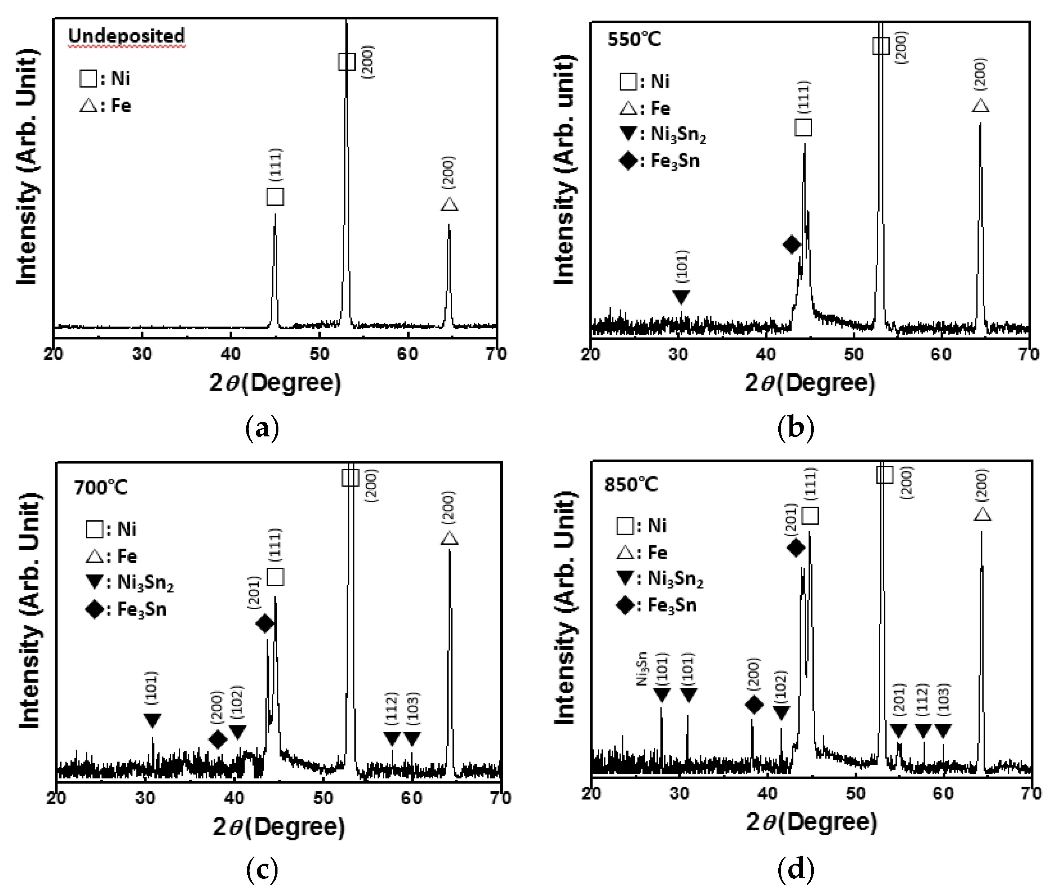
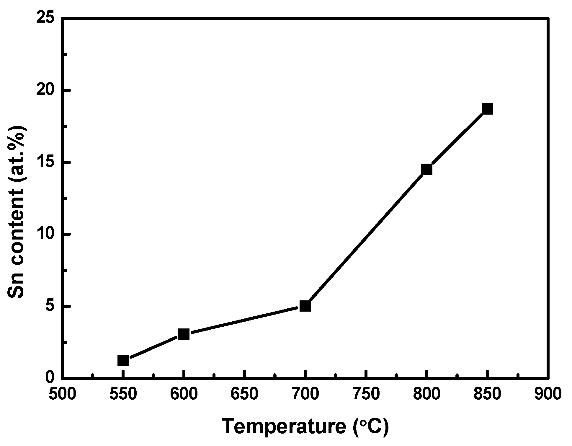
3. Results and Discussion

Figure 2 shows the electrical resistivities of Ni–Fe wires on which Sn was deposited through LPCVD at different deposition temperatures, from 550 to 850 °C. The diamond symbol defined as “undeposited” in the figure represents a pristine Ni–Fe wire, without Sn. The resistivity of a pristine Ni–Fe wire was 39.5 μΩ⋅cm. When Sn was deposited on a Ni–Fe wire, the wire’s resistivity changed. The resistivity increased slightly to 39.7 μΩ⋅cm when Sn was deposited at 550 °C and increased monotonically with the deposition temperature. For Sn deposition at 850 °C, the resistivity of the Ni–Fe wire was 43.2 μΩ⋅cm, which was 9.4% higher than that of the pristine Ni–Fe wire. This indicated that LPCVD of Sn on Ni–Fe wires can be used to manipulate the resistivity of Ni–Fe alloys. In particular, the resistivity of Sn-deposited Ni–Fe wires depends on the deposition temperature. To check whether annealing itself affects the resistivity of the Ni–Fe wires, the resistivityof the pristine Ni–Fe wire was measured at 550 and 850 °C and resulted to be 39.5 and 39.4 μΩ⋅cm at 550 and 850 °C, respectively, whichis nearly the same as that of the pristine Ni–Fe wire before annealing. This implies that annealing barely affects the resistivity of Ni–Fe wires in the absence of Sn deposition.
The electrical resistivity of a material indicates how strongly the material resists the migration of electrons in it. Therefore, the resistivity depends on the structure and morphology of a material. In order to investigate the change in resistivity of the Sn-deposited Ni–Fe wires depending on their structure and morphology, XRD and SEM measurements were performed.
Figure 3 shows the XRD spectra of the Ni–Fe wires deposited with Sn at the temperatures of 550, 700, and 850 °C. The X-ray pattern of the pristine Ni–Fe wire is also shown. The pristine Ni–Fe wire showed distinct Ni peaks (JCPDS card no. 88-2326) [16,17] and a Fe peak (JCPDS card no. 06-0696) [18] (Figure 3a). For Ni–Fe wires deposited with Sn, other peaks appeared. At the deposition temperature of 550 °C, small peaks corresponding to Ni3Sn2 (JCPDS card no. 06-0414) [19,20,21] and Fe3Sn (JCPDS card no. 65-9135) [22,23] could be observed (Figure 3b). The intensities of these peaks increased with the deposition temperature, implying that the formation of Ni3Sn2 and Fe3Sn, which are the reaction products of LPCVD of Sn on Ni–Fe, increased the resistivity of Ni–Fe wires. The formation of intermetallic phases such as NiSn3, Ni3Sn2, Ni3Sn4, and FeSn2 was also observed when Sn was electrodeposited on Ni–Fe wires [24].
The formation of reaction products on the Ni–Fe wires during LPCVD of Sn was supported by SEM measurements. Figure 4 shows SEM images of the Ni–Fe wires after Sn deposited at 550, 700, and 850 °C. The SEM image of the pristine Ni–Fe wire is also shown for comparison. The surface of the pristine Ni–Fe wire looked smooth (Figure 4a). The Ni–Fe wire after Sn deposition at 550 °C was covered with particulates with a highly uniform nodular structure (Figure 4b). The particulates coalesced and increased in size with the increase of the deposition temperature, because their growth was more rapid at higher temperatures. Finally, at the deposition temperature of 850 °C, the Sn-deposited Ni–Fe wire was covered with large particulates having irregular shapes. These particulates (identified as Ni3Sn2 and Fe3Sn from the XRD spectra) were discretely distributed, and pores of various sizes were observed (Figure 4d).
When the surface of a material is covered with particulates, electrons may be scattered by the particulates, resulting in a decrease in the mean free path of the electrons [25,26]. As observed in the XRD spectra and SEM images, Ni3Sn2 and Fe3Sn particulates formed on the surface of Ni–Fe wires after Sn deposition. These particulates acted as scattering sites and inhibited electron transport. This increased the electrical resistivity of the Sn-deposited Ni–Fe wires. An increase in the resistivity of Ni and Fe following the formation of Ni–Sn and Fe–Sn alloys has been reported previously [5,27].
Since the particulates contained Sn, it may be expected that the resistivity of the Sn-deposited Ni–Fe wire would be directly correlated with the amount of Sn on it. A compositional analysis of the Sn-deposited Ni–Fe wires was performed to verify this. Figure 5 shows the atomic Sn content of the Ni–Fe wires at deposition temperatures from 550 to 850 °C. The atomic Sn content was 1.24% t the deposition temperature of 550 °C and it increased with the deposition temperature, reaching 18.72% at 850 °C. Interestingly, the increase in the atomic Sn content was more rapid at temperatures above 700 °C. This may be attributed to the requirement of a high temperature for the efficient reaction between Fe and Sn. It has been reported that for the formation of alloys of Fe and Sn, temperatures higher than 700 °C are required. [28].
For the Sn-deposited Ni–Fe wires, the temperature dependency of the Sn content was very similar to that of the resistivity (see Figure 2). This implies that the atomic Sn content directly affects the resistivity of the wires when Sn is deposited through LPCVD.
To determine the Sn content across the sample, a depth profile experiment was carried out using ToF-SIMS and is shown in Figure 6. For ToF-SIMS measurements, an Sn-deposited Ni foil was used as a sample because the cylindrical Ni–Fe wire was not appropriate for depth profiling. Sn was deposited on the Ni foil through LPCVD at 850 °C. Other process conditions for the deposition of Sn on the Ni foil were the same as those for the deposition of Sn on Ni–Fe wires: Ar flow rate = 50 sccm, chamber pressure = 4 Torr, and deposition time = 1 h. As seen in Figure 6, the Sn content decreased with increasing depth from the surface of the Ni foil and was not detected beyond 150 nm in depth. Since the Sn content of the Ni–Fe wires increased with the deposition temperature, it is expected that Sn cannot penetrate the Ni–Fe wire beyond 150 nm at deposition temperatures lower than 850 °C. Therefore, it can be said that the formation of particulates due to Sn deposition occurred mainly on the surface of the Ni–Fe wire.

4. Conclusions

Sn was deposited on Ni–Fe wires through LPCVD to modulate the electrical resistivity of the wires. Sn was deposited at temperatures from 550 to 850 °C, and the Sn-deposited Ni–Fe wires were subjected to structural, morphological, and compositional analyses.
The resistivity of the Sn-deposited Ni–Fe wires increased monotonically with the deposition temperature. At the highest temperature used in this study (850 °C), the resistivity of the Ni–Fe wires was 43.2 μΩ⋅cm, which was 9.4% higher than that of the pristine Ni–Fe wire. A structural analysis based on XRD measurements showed that peaks representing components other than Ni and Fe appeared when Sn was deposited on a Ni–Fe wire. These peaks were identified as corresponding to Ni3Sn2 and Fe3Sn, and their intensity increased with the deposition temperature. A morphological examination based on SEM measurements showed that when Sn was deposited on a Ni–Fe wire, the surface of the wire became covered with particulates. These particulates coalesced and increased in size with an increase in the deposition temperature. A compositional investigation based on EDX measurements showed that the atomic Sn content increased with the deposition temperature. For the Sn-deposited Ni–Fe wires, the temperature dependency of the Sn content was very similar to that of the resistivity, implying that the atomic Sn content directly affected the resistivity when Sn was deposited through LPCVD.
The results of this work suggest that LPCVD of Sn on Ni–Fe wires could be used to manipulate the electrical resistivity of the wires, which correspondingly could be employed for the fabrication of fusing resistors.

Author Contributions

Conceptualization, J.-H.K. and C.-K.K.; Methodology, J.-H.K. and J.G.B.; Software, J.-H.K. and J.G.B.; Validation, J.-H.K. and J.G.B.; Formal Analysis, J.-H.K. and J.G.B.; Investigation, J.-H.K. and J.G.B.; Resources, J.-H.K. and J.G.B.; Data Curation, J.-H.K. and J.G.B.; Writing—Original Draft Preparation, C.-K.K.; Writing—Review & Editing, C.-K.K.; Visualization, J.-H.K. and J.G.B.; Supervision, C.-K.K.; Project Administration, C.-K.K.; Funding Acquisition, C.-K.K. All authors have read and agreed to the published version of the manuscript.

Funding

This work was supported by the Korea Institute of Energy Technology Evaluation and Planning (KETEP) grant funded by the Korea Government Ministry of Trade, Industry and Energy (Grant No. 20172010104830) and the National Research Foundation of Korea (NRF) grant funded by the Korea government (MEST) (grant No. 2018R1A2B6002410).

Conflicts of Interest

The authors declare no conflict of interest.

References

  1. Zhang, S.; Xu, Z.; Chen, S.; Xu, Y.; Wu, G. The design principle and application of power resistor with over temperature and over current protection function. Adv. Mat. Res. 2012, 562, 1501–1504. [Google Scholar] [CrossRef]
  2. Schroeder, K. Fail-safe wirewound resistors for robust applications. Power Electron. Technol. 2010, 36, 41–43. [Google Scholar]
  3. Kurosawa, H.; Tomimuro, H. Hybrid integrated surge protector for digital switching system. IEEE Trans. Compon. HybridsManuf. Technol. 1985, 8, 259–263. [Google Scholar] [CrossRef]
  4. Yao, Y.D.; Chen, Y.Y.; Tzeng, S.J.; Chuang, T.H. Electrical resistivity, magnetization, and grain boundary precipitates in Ni-Sn alloys. Phys. Status Solidi A Appl. Mat. 1990, 121, 213–218. [Google Scholar] [CrossRef]
  5. Geny, J.F.; Marchal, G.; Mangin, P.; Janot, C.H.R.; Piecuch, M. Structure, forming ability, and electrical-transport properties of isotypical amorphous alloys MxSn1−x (M = Fe, Co, Ni). Phys. Rev. B 1982, 25, 7449–7466. [Google Scholar] [CrossRef]
  6. Bailey, W.; Kabos, P.; Mancoff, F.; Russek, S. Control of magnetization dynamics in Ni81Fe19 thin films through the use of rare-earth dopants. IEEE Trans. Magn. 2001, 37, 1749–1754. [Google Scholar] [CrossRef] [Green Version]
  7. Kim, J.H.; Cho, S.W.; Kang, D.W.; Lee, K.M.; Baek, C.Y.; Lee, H.M.; Kim, C.K. Electrical, structural, and morphological characteristics of dopantless tin oxide films prepared by low pressure chemical vapor deposition. Sci. Adv. Mater. 2016, 8, 117–121. [Google Scholar] [CrossRef]
  8. Kim, J.H.; Lee, H.M.; Kang, D.W.; Lee, K.M.; Kim, C.K. Effect of oxygen flow rate on the electrical and optical characteristics of dopantless tin oxide films fabricated by LPCVD. Korean J. Chem. Eng. 2016, 33, 2711–2715. [Google Scholar] [CrossRef]
  9. Vernardou, D.; Psifis, K.; Louloudakis, D.; Papadimitropoulos, G.; Davazoglou, D.; Katsarakis, N.; Koudoumas, E. Low Pressure CVD of Electrochromic WO3 at 400 °C. J. Electrochem. Soc. 2015, 162, H579–H582. [Google Scholar] [CrossRef]
  10. Kim, H.T.; Lee, S.Y.; Lee, H.R.; Park, C.H. Effects of growth temperature on titanium carbide (TiC) film formation using low-frequency (60 Hz) plasma-enhanced chemical vapor deposition. Korean J. Chem. Eng. 2018, 35, 246–250. [Google Scholar] [CrossRef]
  11. Li, J.; Qin, H.; Liu, Y.; Ye, F.; Li, Z.; Cheng, L.; Zhang, L. Effect of the SiCl4 flow rate on SiBN deposition kinetics in SiCl4-BCl3-NH3-H2-Ar environment. Materials 2017, 10, 627. [Google Scholar] [CrossRef] [PubMed] [Green Version]
  12. Li, J.; Zhao, M.; Liu, Y.; Chai, N.; Ye, F.; Qin, H.; Cheng, L.; Zhang, L. Microstructure and dielectric properties of LPCVD/CVI-SiBCN ceramics annealed at different temperatures. Materials 2017, 10, 655. [Google Scholar] [CrossRef] [PubMed] [Green Version]
  13. Liu, X.; Sun, G.; Liu, B.; Yan, G.; Guan, M.; Zhang, Y.; Zhang, F.; Chen, Y.; Dong, L.; Zheng, L.; et al. Growth of hexagonal columnar nanograin structured SiC thin films on silicon substrates with graphene-graphitic carbon nanoflakes templates from solid carbon sources. Materials 2013, 6, 1543–1553. [Google Scholar] [CrossRef] [Green Version]
  14. Zhao, X.; Wang, X.; Xin, H.; Zhang, L.; Yang, J.; Jiang, G. Controllable preparation of SiC coating protecting carbon fiber from oxidation damage during sintering process and SiC coated carbon fiber reinforced hydroxyapatite composites. Appl. Surf. Sci. 2018, 450, 265–273. [Google Scholar] [CrossRef]
  15. Yang, M.; Sasaki, S.; Suzuki, K.; Miura, H. Control of the nucleation and quality of graphene grown by low-pressure chemical vapor deposition with acetylene. Appl. Surf. Sci. 2016, 366, 219–226. [Google Scholar] [CrossRef]
  16. Cheng, C.; Zheng, F.; Zhang, C.; Du, C.; Fang, Z.; Zhang, Z.; Chen, W. High-efficiency bifunctional electrocatalyst based on 3D freestanding Cu foam in situ armored CoNi alloy nanosheet arrays for overall water splitting. J. Power Sources 2019, 427, 184–193. [Google Scholar] [CrossRef]
  17. Ni, W.; Wang, B.; Cheng, J.; Li, X.; Guan, Q.; Guab, G.; Huang, L. Hierarchical foam of exposed ultrathin nickel nanosheets supported on chainlike Ni-nanowires and the derivative chalcogenide for enhanced pseudocapacitance. Nanoscale 2014, 6, 2618–2623. [Google Scholar] [CrossRef] [Green Version]
  18. Li, Y.; Cao, Y.; Jia, D. Facile solid-state synthesis of Fe/FeOOH hierarchical nanostructures assembled from ultrathin nanosheets and their application in water treatment. Cryst. Eng. Comm. 2016, 18, 8465–8471. [Google Scholar] [CrossRef]
  19. Astuti, M.D.; Hara, T.; Ichikuni, N.; Shimazu, S. One-pot selective conversion of C5-furan into 1,4-pentanediol over bulk Ni-Sn alloy catalysts in an ethanol/H2O solvent mixture. Green Chem. 2019, 21, 2307–2315. [Google Scholar]
  20. Kim, D.; Lee, D.; Kim, J.; Moon, J. Electrospun Ni-added SnO2–carbon nanofiber composite anode for high-performance lithium-ion batteries. ACS Appl. Mater. Interfaces 2012, 4, 5408–5415. [Google Scholar] [CrossRef] [PubMed]
  21. Barakat, N.A.M.; Abdelkareem, M.A.; Abdelghani, E.A.M. Influence of Sn content, nanostructural morphology, and synthesis temperature on the electrochemical active area of Ni-Sn/C nanocomposite: Verification of methanol and urea electrooxidation. Catalysts 2019, 9, 330. [Google Scholar] [CrossRef] [Green Version]
  22. Shi, H.; Zhang, A.; Zhang, X.; Yin, H.; Wang, S.; Tang, Y.; Zhou, Y.; Wu, P. Pyrolysis of cyano-bridged hetero-metallic aerogels: A general route to immobilize Sn–M (M = Fe, Ni) alloys within a carbon matrix for stable and fast lithium storage. Nanoscale 2018, 10, 4962–4968. [Google Scholar] [CrossRef] [PubMed]
  23. Sales, B.C.; Saparov, B.; McGuire, M.A.; Singh, D.J.; Parker, D.S. Ferromagnetism of Fe3Sn and alloys. Sci. Rep. 2014, 4, 1–6. [Google Scholar] [CrossRef] [PubMed] [Green Version]
  24. Vitina, I.; Pelece, I.; Rubene, V.; Belmane, V.; Lubane, M.; Krumina, A.; Zarina, Z. Formation of intermediate intermetallic layers on interaction of electrodeposited Sn, Ni-Fe, Ni-B coatings with different metallic substrate. J. Adhes. Sci. Technol. 1997, 11, 835–860. [Google Scholar] [CrossRef]
  25. Choe, G.; Steinback, M. Surface roughness effects on magnetoresistive and magnetic properties of NiFe thin films. J. Appl. Phys. 1999, 85, 5777–5779. [Google Scholar] [CrossRef]
  26. Tang, W.; Xu, K.; Wang, P.; Li, X. Surface roughness and resistivity of Au films on Si-(111) substrate. Microelectron. Eng. 2003, 66, 445–450. [Google Scholar] [CrossRef]
  27. Onda, A.; Komatsu, T.; Yashima, T. Preparation and catalytic properties of single-phase Ni–Sn intermetallic compound particles by CVD of Sn(CH3)4 onto Ni/Silica. J. Catal. 2001, 201, 13–21. [Google Scholar] [CrossRef]
  28. Trumpy, G.; Both, E.; Djega-Mariadassou, C.; Lecocq, P. Mossbauer-effect studies of iron-tin alloys. Phys. Rev. B 1970, 2, 3477–3490. [Google Scholar] [CrossRef] [Green Version]
Figure 1. Schematic of the low-pressure chemical vapor deposition (LPCVD) apparatus used for the deposition of Sn on Ni–Fe wires.
Coatings 10 00317 g001
Figure 2. Electrical resistivity of Sn-deposited Ni–Fe wires as a function of the deposition temperature. The diamond symbol defined as “undeposited” indicates a pristine Ni–Fe wire, without Sn. The resistivity was measured at room temperature.
Coatings 10 00317 g002
Figure 3. (a) XRD spectrum of the pristine wire. XRD spectra of Ni–Fe wires after Sn deposition of at (b) 550 °C, (c) 700 °C, and (d) 850 °C.
Coatings 10 00317 g003
Figure 4. (a) SEM image of the pristine wire. SEM images of Ni–Fe wires after Sn deposition at (b) 550 °C, (c) 700 °C, and (d) 850 °C.
Coatings 10 00317 g004
Figure 5. Atomic Sn content of Ni–Fe wires as a function of the deposition temperature.
Coatings 10 00317 g005
Figure 6. Time-of-flight secondary-ion mass spectrometer (ToF-SIMS) depth profile of Sn deposited on a Ni foil. Sn was deposited on the Ni foil through LPCVD at 850 °C.
Coatings 10 00317 g006

