One-Step Synthesis of Graphene, Copper and Zinc Oxide Graphene Hybrids via Arc Discharge: Experiments and Modeling

 ,
,
Abstract
1. Introduction
2. Materials and Methods
2.1. Materials
2.2. Characterization Techniques
2.3. Methods
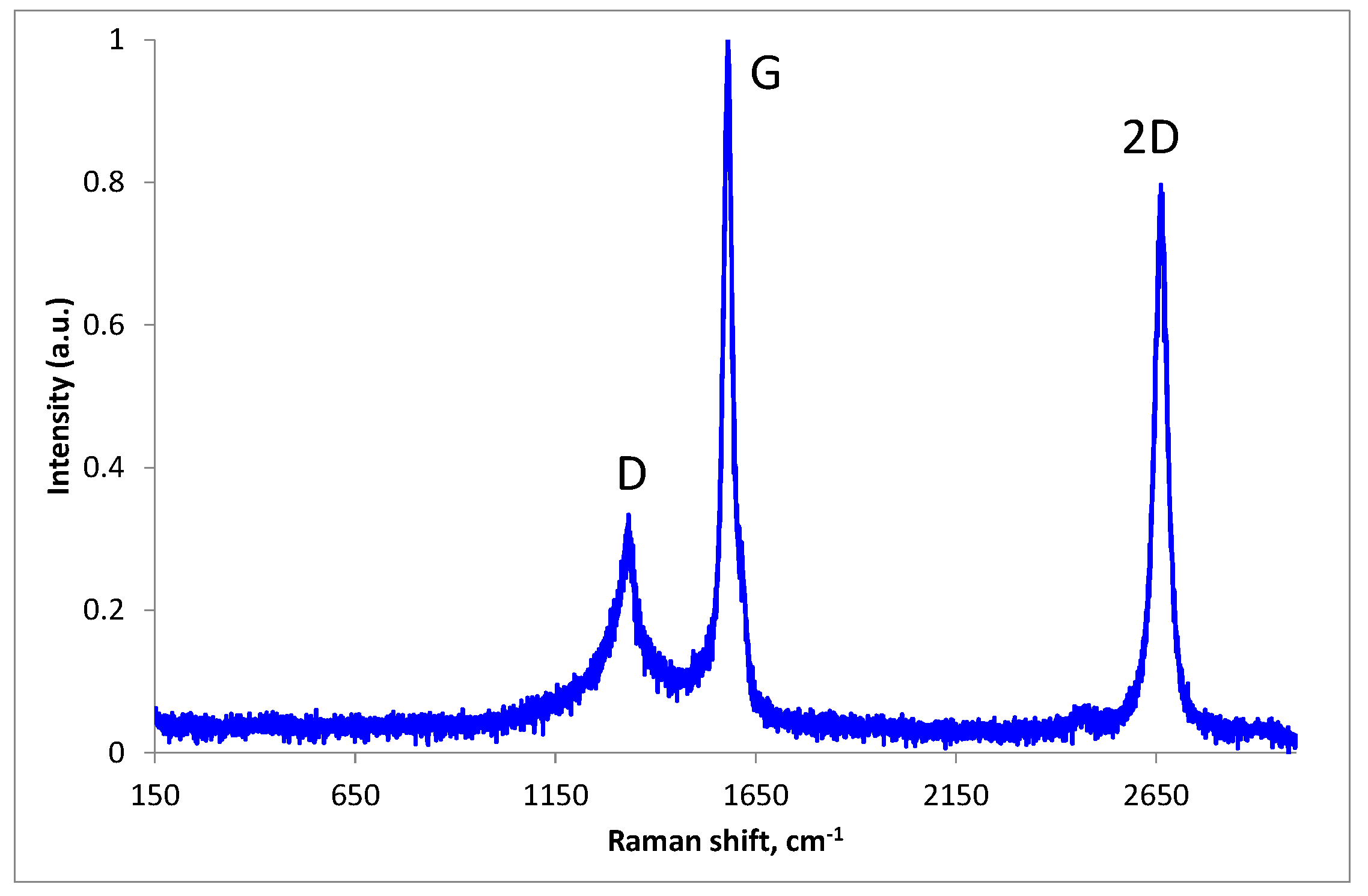
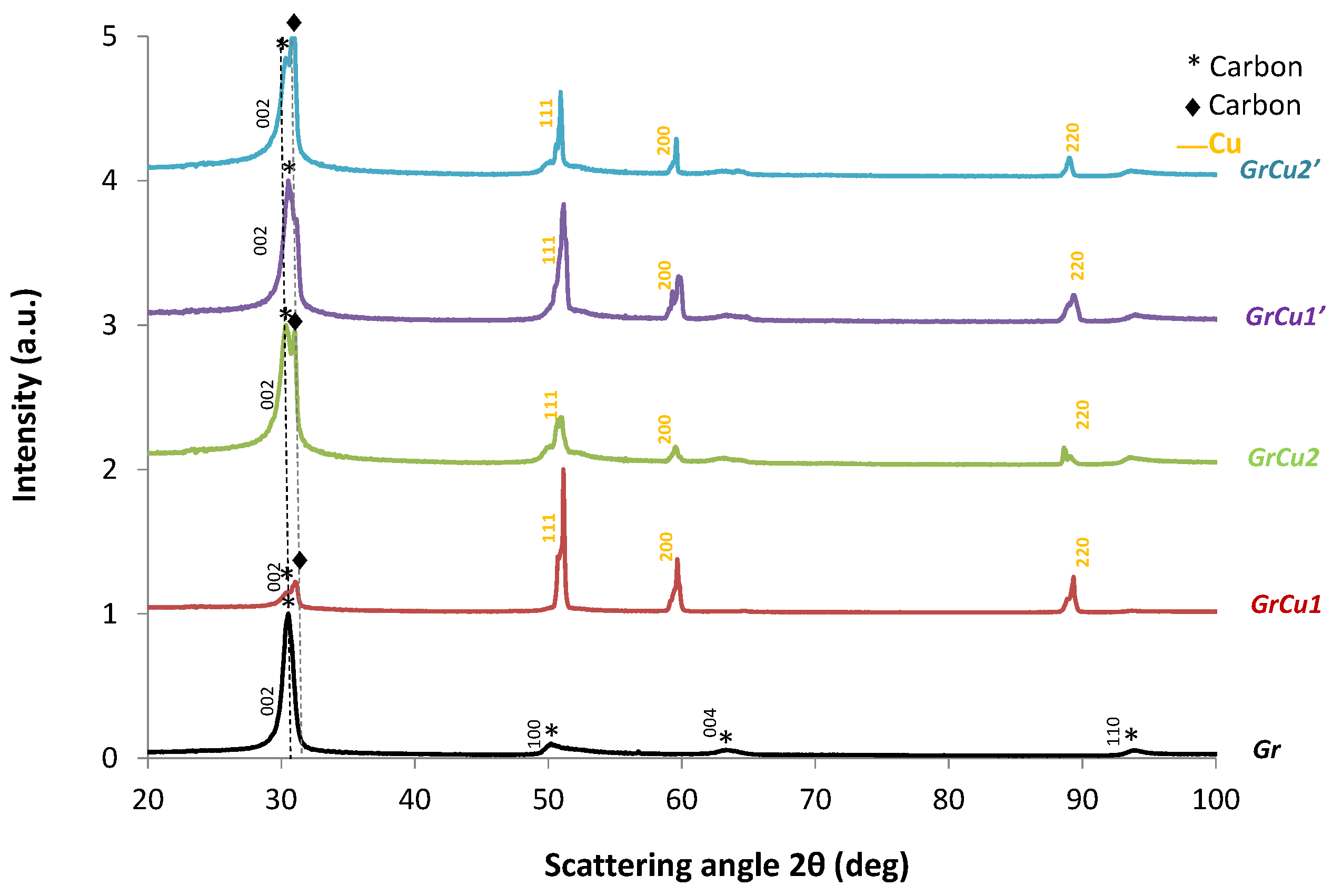
3. Results
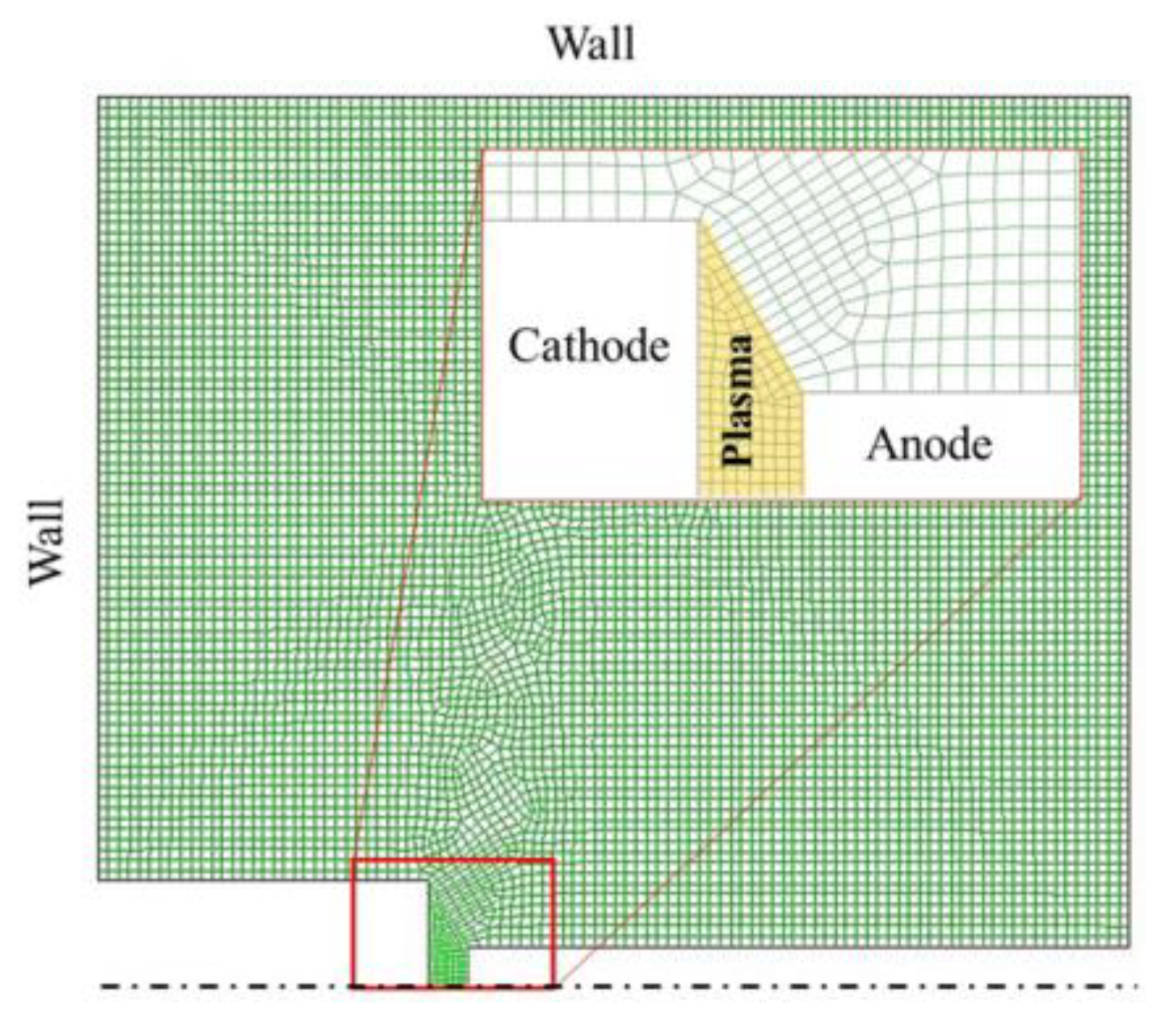
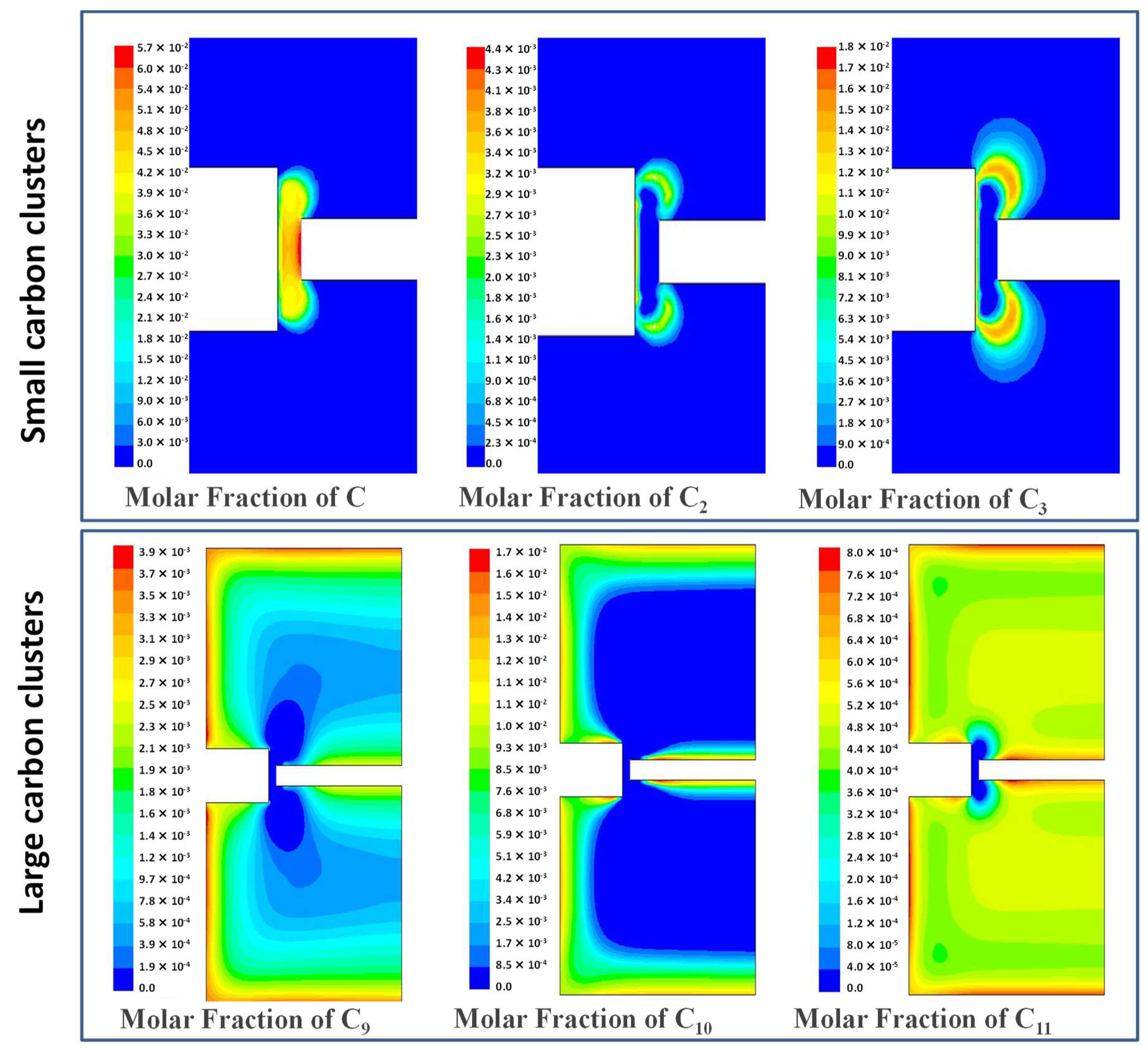
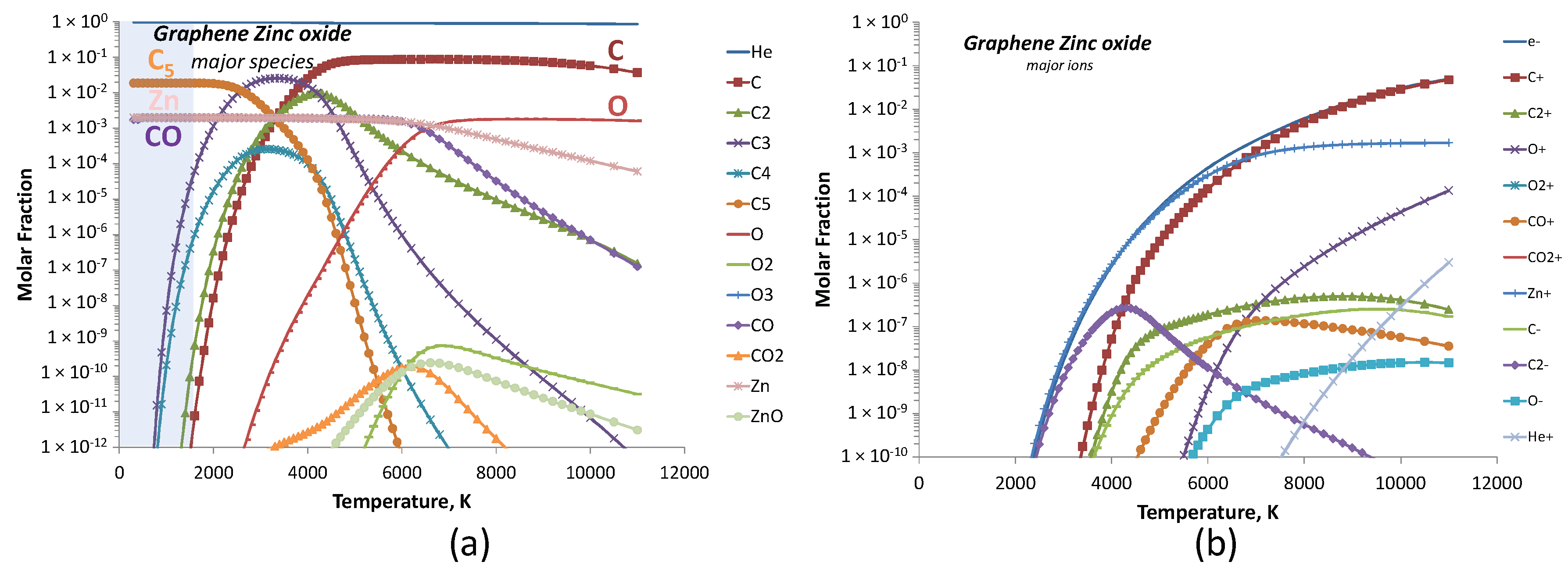
4. Modeling
5. Conclusions
Author Contributions
Funding
Acknowledgments
Conflicts of Interest
References
- Novoselov, K.S.; Geim, A.K.; Morozov, S.V.; Jiang, D.; Zhang, Y.; Dubonos, S.V.; Grigorieva, I.V.; Firsov, A.A. Electric field effect in atomically thin carbon films. Science 2004, 306, 666–669. [Google Scholar] [CrossRef] [PubMed]
- Balandin, A.A. Thermal properties of graphene and nanostructured carbon materials. Nat. Mater. 2011, 10, 569–581. [Google Scholar] [CrossRef] [PubMed]
- Iakunkov, A.; Skrypnychuk, V.; Nordenström, A.; Shilayev, E.A.; Korobov, M.; Prodana, M.; Enachescu, M.; Larsson, S.H.; Talyzin, A.V. Activated graphene as a material for supercapacitor electrodes: Effects of surface area, pore size distribution and hydrophilicity. Phys. Chem. Chem. Phys. 2019, 21, 17901–17912. [Google Scholar] [CrossRef] [PubMed]
- Banszerus, L.; Sohier, T.; Epping, A.; Winkler, F.; Libisch, F.; Haupt, F.; Watanabe, K.; Taniguchi, T.; Müller-Caspary, K.; Marzari, N.; et al. Extraordinary high room-temperature carrier mobility in graphene-WSe2 heterostructures. arXiv 2019, arXiv:1909.09523. [Google Scholar]
- Kim, S.H.; Song, W.; Jung, M.W.; Kang, M.-A.; Kim, K.; Chang, S.-J.; Lee, S.S.; Lim, J.; Hwang, J.; Myung, S.; et al. Carbon Nanotube and graphene hybrid thin film for transparent electrodes and field effect transistors. Adv. Mater. 2014, 26, 4247–4252. [Google Scholar] [CrossRef]
- Badhulika, S.; Thakoor, T.T.; Villarreal, C.; Mulchandani, A. Graphene hybrids: Synthesis strategies and applications in sensors and sensitized solar cells. Front. Chem. 2015, 3, 38. [Google Scholar] [CrossRef]
- Hidalgo-Manrique, P.; Lei, X.; Xu, R.; Zhou, M.; Kinloch, I.A.; Young, R.J. Copper/graphene composites: A review. J. Mater. Sci. 2019, 54, 12236–12289. [Google Scholar] [CrossRef]
- Xiao, Q.; Yi, X.; Jiang, B.; Qin, Z.; Hu, J.; Jiang, Y.; Liu, H.; Wang, B.; Yi, D. In-situ synthesis of graphene on surface of copper powder by rotary CVD and its application in fabrication of reinforced Cu-matrix composites. Adv. Mater. Sci. 2017, 2, 5–6. [Google Scholar] [CrossRef]
- Cseri, L.; Baugh, J.; Alabi, A.; AlHajaj, A.; Zou, L.; Dryfe, R.A.W.; Budd, P.M.; Szekely, G. Graphene oxide-polybenzimidazolium nanocomposite anion exchange membranes for electrodialysis. J. Mater. Chem. A 2018, 6, 24728. [Google Scholar] [CrossRef]
- Kweon, H.; Lin, C.W.; Hasan, M.M.F.; Kaner, R.; Sant, G.N. Highly permeable polyaniline-graphene oxide nanocomposite membranes for CO2 separations. ACS Appl. Polym. Mater. 2019, 1, 12. [Google Scholar] [CrossRef]
- Fei, F.; Cseri, L.; Szekely, G.; Blanford, C.F. Robust covalently crosslinked polybenzimidazole/graphene oxide membranes for high-flux organic solvent nanofiltration. ACS Appl. Mater. Interfaces 2018, 10, 18. [Google Scholar] [CrossRef] [PubMed]
- Vallés, C.; Zhang, X.; Cao, J.; Lin, F.; Young, R.J.; Lombardo, A.; Ferrari, A.C.; Burk, L.; Rolf Mülhaupt, R.; Kinloch, I.A. Graphene/polyelectrolyte layer-by-layer coatings for electromagnetic interference shielding. ACS Appl. Nano Mater. 2019, 2, 5272–5281. [Google Scholar] [CrossRef]
- Zhu, Y.; Li, J.; Yun, X.; Zhou, W.; Xi, L.; Li, N.; Hu, Z. Hydrothermal synthesis of nanoflakes-assembled (Ni0.5Co0.5)0.85Se microspheres as cathode and reduced graphene oxide/porous Fe2O3 nanospheres composite as anode for novel alkaline aqueous batteries. ACS Sustain. Chem. Eng. 2020, 8, 561–572. [Google Scholar] [CrossRef]
- Kong, W.; Liu, F.; Liu, Y. Design of nitrogen-doped graphitized 2D hierarchical porous carbons as efficient solid base catalysts for transesterification to biodiesel. Green Chem. 2020, 22, 903–912. [Google Scholar] [CrossRef]
- Prasad, K.P.; Chen, Y.; Chen, P. Three-dimensional graphene-carbon nanotube hybrid for high-performance enzymatic biofuel cells. ACS Appl. Mater. Interfaces 2014, 6, 3387–3393. [Google Scholar] [CrossRef] [PubMed]
- Dong, X.; Wang, X.; Wang, L.; Song, H.; Zhang, H.; Huang, W.; Chen, P. 3D Graphene foam as a monolithic and macroporous carbon electrode for electrochemical sensing. ACS Appl. Mater. Interfaces 2012, 4, 3129–3133. [Google Scholar] [CrossRef]
- Hwa, K.-Y.; Subramani, B. Synthesis of zinc oxide nanoparticles on graphene-carbon nanotube hybrid for glucose biosensor applications. Biosens. Bioelectron. 2014, 62, 127–133. [Google Scholar] [CrossRef]
- Li, Y.F.; Dong, F.X.; Chen, Y.; Zhang, X.L.; Wang, L.; Bi, Y.G.; Tian, Z.N.; Liu, Y.F.; Feng, J.; Sun, H.B. As-grown graphene/copper nanoparticles hybrid nanostructures for enhanced intensity and stability of surface plasmon resonance. Sci. Rep. 2016, 6, 37190. [Google Scholar] [CrossRef]
- Cho, B.; Yoonb, J.; Hahm, M.G.; Kim, D.H.; Kim, A.R.; Kahng, Y.H.; Park, S.W.; Lee, Y.-J.; Park, S.-G.; Kwon, J.-D.; et al. Graphene-based gas sensor: Metal decoration effect and application to a flexible device. J. Mater. Chem. C2 2014, 2, 5280–5285. [Google Scholar] [CrossRef]
- Echtermeyer, T.J.; Britnell, L.; Jasnos, P.K.; Lombardo, A.; Gorbachev, R.V.; Grigorenko, A.N.; Geim, A.K.; Ferrari, A.C.; Novoselov, K.S. Strong plasmonic enhancement of photovoltage in graphene. Nat. Commun. 2011, 2, 458. [Google Scholar] [CrossRef]
- Emani, N.K.; Chung, T.F.; Ni, X.; Kildishev, A.V.; Chen, Y.P.; Boltasseva, A. Electrically tunable damping of plasmonic resonances with graphene. Nano Lett. 2012, 12, 5202–5206. [Google Scholar] [CrossRef] [PubMed]
- Engel, M.; Steiner, M.; Lombardo, A.; Ferrari, A.C.; Löhneysen, H.V.; Avouris, P.; Krupke, R. Light-matter interaction in a microcavity-controlled graphene transistor. Nat. Commun. 2012, 3, 906. [Google Scholar] [CrossRef] [PubMed]
- Li, X.H.; Choy, W.C.H.; Ren, X.G.; Zhang, D.; Lu, H.F. Highly intensity surface enhanced raman scattering by usinig monolayer graphene as the nanospacer of metal film-metal nanoparticle coupling system. Adv. Funct. Mater. 2014, 24, 3114–3122. [Google Scholar] [CrossRef]
- Reckinger, N.; Vlad, A.; Melinte, S.; Colomer, J.F.; Sarrazin, M. Graphene-coated holey metal films: Tunable molecular sensing by surface plasmon resonance. Appl. Phys. Lett. 2013, 102, 211108. [Google Scholar] [CrossRef]
- Xu, M.; Feng, J.; Liu, Y.S.; Jin, Y.; Wang, H.Y.; Sun, H.B. Effective and tunable light trapping in bulk heterojunction organic solar cells by employing Au-Ag alloy nanoparticles. Appl. Phys. Lett. 2014, 105, 153303. [Google Scholar] [CrossRef]
- Leem, J.; Wang, M.C.; Kang, P.; Nam, S. Mechanically self-assembled, three-dimensional graphene-gold hybrid nanostructures for advanced nanoplasmonic sensors. Nano Lett. 2015, 15, 7684–7690. [Google Scholar] [CrossRef]
- Xie, H.; Lee, H.Y.; Youn, W.; Choi, M. Nanofluids containing multiwalled carbon nanotubes and their enhanced thermal conductivities. J. Appl. Phys. 2003, 94, 4967–4971. [Google Scholar] [CrossRef]
- Green, M.; Chen, X. Recent progress of nanomaterials for microwave absorption. JMAT 2019, 5, 503–541. [Google Scholar] [CrossRef]
- Hosni, M.; Kusumawati, Y.; Farhat, S.; Jouini, N.; Pauporté, T. Effects of oxide nanoparticle size and shape on electronic structure, charge transport, and recombination in dye-sensitized solar cell photoelectrodes. J. Phys. Chem. C 2013, 118, 16791–16798. [Google Scholar] [CrossRef]
- Liu, J.W.; Wu, J.; Ahmad, M.Z.; Wlodarski, W. Hybrid aligned zinc oxide nanowires array on CVD graphene for hydrogen sensing. In Proceedings of the 2013 Transducers & Eurosensors XXVII: 17th International Conference on Solid State Sensors, Actuators and Microsystems (Transducers & Eurosensors XXVII), Barcelona, Spain, 16–20 June 2013; pp. 194–197. [Google Scholar]
- Yi, J.; Lee, J.M.; Park, W. Vertically aligned ZnO nanorods and graphene hybrid architectures for high-sensitive flexible gas sensors. Sens. Actuators B 2011, 155, 264–269. [Google Scholar] [CrossRef]
- Cuong, T.V.; Pham, V.H.; Chung, J.S.; Shin, E.W.; Yoo, D.H.; Hahn, S.H.; Huh, J.S.; Rue, G.H.; Kim, E.J.; Hur, S.H.; et al. Solution-processed ZnO-chemically converted graphene gas sensor. Mater. Lett. 2010, 64, 2479–2482. [Google Scholar] [CrossRef]
- Khan, M.E.; Khan, M.M.; Cho, M.H. Fabrication of WO3 nanorods on graphene nanosheets for improved visible light-induced photocapacitive and photocatalytic performance. RSC Adv. 2016, 6, 20824–20833. [Google Scholar] [CrossRef]
- Mohammada, A.; Khan, M.E.; Karima, M.R.; Choa, M.H. Synergistically effective and highly visible light responsive SnO2-g-C3N4 nanostructures for improved photocatalytic and photoelectrochemical performance. Appl. Surf. Sci. 2019, 495, 143432. [Google Scholar] [CrossRef]
- Hummers, W.S.; Offeman, J.R.E. Preparation of graphitic oxide. J. Am. Chem. Soc. 1958, 80, 1339. [Google Scholar] [CrossRef]
- Khan, M.E.; Khan, M.M.; Cho, M.H. Defected graphene nano-platelets for enhanced hydrophilic nature and visible light-induced photoelectrochemical performances. J. Phys. Chem. Solids 2017, 104, 233–242. [Google Scholar] [CrossRef]
- Li, X.; Cai, W.; An, J.; Kim, S.; Nah, J.; Yang, D.; Piner, R.; Velamakanni, A.; Jung, I.; Tutuc, E.; et al. Large-area synthesis of high-quality and uniform graphene films on copper foils. Science 2009, 324, 1312–1314. [Google Scholar] [CrossRef]
- Kim, E.; An, H.; Jang, H.; Cho, W.J.; Lee, N.; Lee, W.G.; Jung, J. Growth of few-layer graphene on a thin cobalt film on a Si/SiO2 substrate. Chem. Vap. Depos. 2011, 17, 9–14. [Google Scholar] [CrossRef]
- Coraux, J.; N’Diaye, T.; Engler, M.; Busse, C.; Wall, D.; Buckanie, N.; Heringdorf, F.J.M.Z.; Gaste, R.V.; Poelsema, B.; Michely, T. Growth of graphene on Ir(111). New J. Phys. 2009, 11, 023006. [Google Scholar] [CrossRef]
- Kim, K.S.; Zhao, Y.; Jang, H.; Lee, S.Y.; Kim, J.M.; Kim, K.S.; Ahn, J.H.; Kim, P.; Choi, J.Y.; Hong, B.H. Large-scale pattern growth of graphene films for stretchable transparent electrodes. Nature 2009, 457, 706–710. [Google Scholar] [CrossRef]
- Reina, A.; Jia, X.; Ho, J.; Nezich, D.; Son, H.; Bulovic, V.; Dresselhaus, M.; Kong, J. Large area, few-layer graphene films on arbitrary substrates by chemical vapor deposition. Nano Lett. 2009, 9, 30–35. [Google Scholar] [CrossRef]
- Won, S.Y.; Ciobanu, C.V.; Petrova, V.; Shenoy, V.B.; Bareno, J.; Gambin, V.; Petroy, I.; Kodambaka, S. Growth of semiconducting graphene on palladium. Nano Lett. 2009, 9, 3985–3990. [Google Scholar] [CrossRef]
- Fujita, T.; Kobayashi, W.; Oshima, C. Novel structures of carbon layers on a Pt(111) surface. Surf. Interface Anal. 2005, 37, 120–123. [Google Scholar] [CrossRef]
- Mehedi, H.A.; Baudrillart, B.; Alloyeau, D.; Mouhoub, O.; Ricolleau, C.; Pham, V.D.; Chacon, C.; Gicquel, A.; Lagoute, J.; Farhat, S. Synthesis of graphene by cobalt-catalyzed decomposition of methane in plasma-enhanced CVD: Optimization of experimental parameters with Taguchi method. J. Appl. Phys. 2016, 120, 065304. [Google Scholar] [CrossRef]
- Pashova, K.; Hinkov, I.; Aubert, X.; Prasanna, S.; Bénédic, F.; Farhat, S. Graphene synthesis by microwave plasma chemical vapor deposition: Analysis of the emission spectra and modeling. Plasma Sources Sci. Technol. 2019, 28, 045001. [Google Scholar] [CrossRef]
- Bacon, R. Growth, structure, and properties of graphite whiskers. J. Appl. Phys. 1960, 31, 283. [Google Scholar] [CrossRef]
- Wiles, P.G.; Abrahamson, J. Carbon fibre layers on arc electrodes—I: Their properties and cool-down behaviour. Carbon 1978, 16, 341. [Google Scholar] [CrossRef]
- Ebbesen, T.W. Carbon Nanotubes, Preparation and Properties; Ebbesen, T.W., Ed.; CRC Press: Boca Raton, FL, USA, 1996. [Google Scholar]
- Krätschmer, W.; Lamb, L.D.; Fostiropoulos, K.; Huffman, D.R. Solid C60: A new form of carbon. Nature 1990, 347, 354–358. [Google Scholar] [CrossRef]
- Iijima, S. Helical microtubules of graphitic carbon. Nature 1991, 354, 56–58. [Google Scholar] [CrossRef]
- Ebbsen, T.W.; Ajayan, P.M. Large-scale synthesis of carbon nanotubes. Nature 1992, 358, 220–222. [Google Scholar] [CrossRef]
- Moravsky, A.P.; Wexler, E.M.; Loutfy, R.O. Growth of carbon nanotubes by arc discharge and laser ablation. In Carbon Nanotubes Science and Applications; Meyyappan, M., Ed.; CRC Press: Boca Raton, FL, USA, 2004; pp. 65–97. [Google Scholar]
- Farhat, S.; Scott, C. Review of the arc process modeling for fullerene and nanotube production. J. Nanosci. Nanotechnol. 2006, 6, 1189–1210. [Google Scholar] [CrossRef]
- Farhat, S.; Lamy de la Chapelle, M.; Loiseau, A.; Scott, C.D.; Lefrant, S.; Journet, C.; Bernier, P. Diameter control of single-walled carbon nanotubes using argon-helium mixture gases. J. Chem. Phys. 2001, 15, 6752–6759. [Google Scholar] [CrossRef]
- Subrahmanyam, K.S.; Panchakarla, L.S.; Govindaraj, A.; Rao, C.N.R. Simple method of preparing graphene flakes by an arc-discharge method. J. Phys. Chem. C 2009, 113, 4257–4259. [Google Scholar] [CrossRef]
- Karmakar, S.; Kulkarni, N.V.; Nawale, A.B.; Lalla, N.P.; Mishra, R.; Sathe, V.G.; Bhoraskar, S.V.; Das, A.K. A novel approach towards selective bulk synthesis of few-layer graphenes in an electric arc. J. Phys. D Appl. Phys. 2009, 42, 115201. [Google Scholar] [CrossRef]
- Wu, Y.; Wang, B.; Ma, Y.; Huang, Y.; Li, N.; Zhang, F.; Chen, Y. Efficient and large-scale synthesis of few-layered graphene using an arc-discharge method and conductivity studies of the resulting films. Nano Res. 2010, 3, 661–669. [Google Scholar] [CrossRef]
- Wang, Z.; Li, N.; Shi, Z.; Gu, Z. Low-cost and large-scale synthesis of graphene nanosheets by arc discharge in air. Nanotechnology 2010, 21, 175602. [Google Scholar] [CrossRef]
- Keidar, M.; Shashurin, A.; Li, J.; Volotskova, O.; Kundrapu, M.; Zhuang, T.S. Arc plasma synthesis of carbon nanostructures: Where is the frontier? J. Phys. D Appl. Phys. 2011, 44, 174006. [Google Scholar] [CrossRef]
- Shen, B.; Ding, J.; Yan, X.; Feng, W.; Li, J.; Xue, Q. Influence of different buffer gases on synthesis of few-layered graphene by arc discharge method. Appl. Surf. Sci. 2012, 258, 4523–4531. [Google Scholar] [CrossRef]
- Huang, L.; Wu, B.; Chen, J.; Xue, Y.; Geng, D.; Guo, Y.; Yu, G.; Liu, Y. Gram-scale synthesis of graphene sheets by a catalytic arc-discharge method. Small 2013, 9, 1330–1335. [Google Scholar] [CrossRef]
- Karmakar, S.; Nawale, A.B.; Lalla, N.P.; Sathe, V.G.; Kolekar, S.K.; Mathe, V.L.; Das, A.K.; Bhoraskar, S.V. Gas phase condensation of few-layer graphene with rotational stacking faults in an electric-arc. Carbon 2013, 55, 209–220. [Google Scholar] [CrossRef]
- Cotula, U.; Parmaka, E.D.S.; Kaykilarlia, C.; Sarayb, O.; Colakc, O.; Uzunsoya, D. Development of high purity, few-layer graphene synthesis by electric arc discharge technique. Acta Phys. Pol. A 2018, 134, 289–291. [Google Scholar] [CrossRef]
- David, R.L. CRC Handbook of Chemistry and Physics, 90th ed.; CRC Press Inc.: Boca Raton, FL, USA, 2009; p. 2804. [Google Scholar]
- Wu, J.B.; Lin, M.L.; Cong, X.; Liu, H.N.; Tan, P.H. Raman spectroscopy of graphene-based materials and its applications in related devices. Chem. Soc. Rev. 2018, 47, 1822–1873. [Google Scholar] [CrossRef] [PubMed]
- Tan, P.H.; Hu, C.Y.; Dong, J.; Shen, W.C.; Zhang, B. Polarization properties, high-order Raman spectra, and frequency asymmetry between Stokes and anti-Stokes scattering of Raman modes in a graphite whisker. Phys. Rev. B 2001, 64, 214301. [Google Scholar] [CrossRef]
- Debbichi, L.; Marco de Lucas, M.C.; Pierson, J.F.; Kruger, P. Vibrational properties of CuO and Cu4O3 from first-principles calculations, and Raman and infrared spectroscopy. J. Phys. Chem. C 2012, 116, 10232–10237. [Google Scholar] [CrossRef]
- Kastner, J.; Pichler, T.; Kuzmany, H.; Curran, S.; Blau, W.; Weldon, D.N.; Delamesiere, M.; Draper, S.; Zandbergen, H. Resonance Raman and infrared spectroscopy of carbon nanotubes. Chem. Phys. Lett. 1994, 221, 53–58. [Google Scholar] [CrossRef]
- Casiraghi, C.; Hartschuh, A.; Qian, H.; Piscanec, S.; Georgi, C.; Fasoli, A.; Novoselov, K.S.; Basko, D.M.; Ferrari, A.C. Raman spectroscopy of graphene edges. Nano Lett. 2009, 9, 1433–1441. [Google Scholar] [CrossRef] [PubMed]
- Subrahmanyam, K.S.; Vivekchand, S.R.C.; Govindaraj, A.; Rao, C.N.R. A study of graphenes prepared by different methods: Characterization, properties and solubilization. J. Mater. Chem. 2008, 18, 1517–1523. [Google Scholar] [CrossRef]
- Athanassiou, E.K.; Grass, R.N.; Stark, W.J. Large-scale production of carbon-coated copper nanoparticles for sensor applications. Nanotechnology 2006, 17, 1668–1673. [Google Scholar] [CrossRef]
- Cançado, L.G.; Takai, K.; Enoki, T.; Endo, M.; Kim, Y.A.; Mizusaki, H.; Speziali, N.L.; Jorio, A. Measuring the degree of stacking order in graphite by Raman spectroscopy. Carbon 2008, 46, 272–275. [Google Scholar] [CrossRef]
- Ferrari, A.C.; Meyer, J.C.; Scardaci, V.; Casiraghi, C.; Lazzeri, M.; Mauri, F.; Piscanec, S.; Jiang, D.; Novoselov, K.S.; Roth, S.; et al. Raman spectrum of graphene and graphene layers. Phys. Rev. Lett. 2006, 97, 187401. [Google Scholar] [CrossRef]
- Robertson, A.W.; Warner, J.H. Hexagonal single crystal domains of few-layer graphene on copper foils. Nano Lett. 2011, 11, 1182–1189. [Google Scholar] [CrossRef]
- Soares, J.R.; Olivero, M.E.; Garin, C.; David, M.V.; Martins, L.G.P.; Almeida, C.A.; Ferreira, E.H.M.; Takai, K.; Enoki, T.; Paniago, R.M.; et al. Structural analysis of polycrystalline graphene systems by Raman spectroscopy. Carbon 2015, 95, 646. [Google Scholar] [CrossRef]
- Pimenta, M.A.; Dresselhaus, G.; Dresselhaus, M.S.; Cancado, L.G.; Jorio, A.; Saitoe, R. Studying disorder in graphite-based systems by Raman spectroscopy. Phys. Chem. Chem. Phys. 2007, 9, 1276–1291. [Google Scholar] [CrossRef] [PubMed]
- Oshima, C.; Nagashima, A. Ultra-thin epitaxial films of graphite and hexagonal boron nitride on solid surfaces. J. Phys. Condens. Matter 1997, 9, 1–20. [Google Scholar] [CrossRef]
- Li, Z.Q.; Lu, C.J.; Xia, Z.P.; Zhou, Y.; Luo, Z. X-ray diffraction patterns of graphite and turbostratic carbon. Carbon 2007, 45, 1686–1695. [Google Scholar] [CrossRef]
- Lutterotti, L. Maud: A Rietveld analysis program designed for the internet and experiment integration. Acta Crystallogr. A 2000, 56, s54. [Google Scholar] [CrossRef]
- Sowa, H.; Ahsbahs, H. High-pressure X-ray investigation of zincite ZnO single crystals using diamond anvils with an improved shape. J. Appl. Crystallogr. 2006, 39, 169–175. [Google Scholar] [CrossRef]
- Desgreniers, S. High-density phases of ZnO: Structural and compressive parameters. Phys. Rev. B 1998, 58, 14102–14105. [Google Scholar] [CrossRef]
- Shashurin, A.; Keidar, M. Synthesis of 2D materials in arc plasmas. J. Phys. D Appl. Phys. 2015, 48, 31400. [Google Scholar] [CrossRef]
- ANSYS Fluent User’s Guide, Release 15.0; ANSYS, Inc.: Canonsburg, PA, USA, 2013.
- Kee, R.J.; Rupley, F.M.; Miller, J.A.; Coltrin, M.E.; Grcar, J.F.; Meeks, E.; Moffat, H.K.; Lutz, A.E.; Lewis, G.D.; Smooke, M.D.; et al. CHEMKIN Collection, Release 3.6; Reaction Design, Inc.: San Diego, CA, USA, 2001. [Google Scholar]
- JANAF. Report NSRDS-NBS: Dow Chemikal Company, Clearinghouse for Federal Scientific and Technical Information; PB168370; Springfield: Virginia, VA, USA, 1965.
- Kee, R.J.; Lewis, G.D.; Warnatz, J.; Miller, J.A. Technical Report SAND86-8426; Sandia National Laboratories: Albuquerque, NM, USA, 1986.
- Gupta, R.; Yos, J.; Thompson, R.; Lee, K. A Review of Reaction Rates and Thermodynamic and Transport Properties for 11-Species Air Model for Chemical and Thermal Non-Equilibrium Calculations to 30000 K; NASARP-1232; NASA Reference Publication: Hampton, VA, USA, 1990.
- Bilodeau, J.F.; Pousse, J.; Gleizes, A. A mathematical model of the carbon arc reactor for fullerene synthesis. Plasma Chem. Plasma Process. 1998, 18, 285–303. [Google Scholar] [CrossRef]
- Krestinin, A.V.; Moravskii, A.P.; Tesner, P.A. A kinetic modeling of formation of fullerenes C60 and C70 in condensation of carbon vapor. Chem. Phys. Rep. 1998, 17, 1687–1707. [Google Scholar]
- Gurvich, L.V.; Iorish, V.S. Ivtanthermo—A Thermodynamic Database and Software System for the Personal Computer. User’s Guide; CRC Press: Boca Raton, FL, USA, 1993. [Google Scholar]


| Experiment 1 | Hybrid filler | Weight%, y | Weight%, Y | Atom%, X | Current (A) |
|---|---|---|---|---|---|
| Gr | - | - | - | - | 120 |
| GrCu1 | Cu | 75 | 11.65 | 2.43 | 120 |
| GrCu2 | Cu | 100 | 20.74 | 4.71 | 120 |
| GrCu1’ | Cu | 75 | 11.65 | 2.43 | 150 |
| GrCu2’ | Cu | 100 | 20.74 | 4.71 | 150 |
| GrZnO | ZnO | 100 | 12.26 | 2.02 | 120 |
| Sample | ID/IG | I2D/IG | La (nm) 1 | ΔLa (nm) | FWMH (cm−1) 2 |
|---|---|---|---|---|---|
| Gr | 0.31 | 0.88 | 124 | 3 | 39.8 |
| GrCu1 | 0.34 | 0.85 | 113 | 2 | 41.8 |
| GrCu2 | 0.55 | 0.36 | 70 | 1 | 53.1 |
| GrCu1’ | 0.27 | 0.76 | 142 | 1 | 38.6 |
| GrCu2’ | 0.3 | 0.58 | 128 | 3 | 30.3 |
| GrZnO | 0.13 | 0.44 | 296 | 13 | 53.4 |
| Sample | 2θ° | Crystal System | Lattice Parameters (Å) | Crystallite Size D (nm) 1 | ||
|---|---|---|---|---|---|---|
| Cu(111) | Cu(200) | Cu(220) | ||||
| GrCu1 | 51.13 | 59.67 | 88.87 | cubic | a = 3.6036 ± 1 × 10⁻⁴ | 53.5 ± 1.1 |
| GrCu2 | 50.98 | 59.53 | 88.61 | cubic | a = 3.6081 ± 2 × 10⁻⁴ | 48.9 ± 2.9 |
| GrCu1’ | 51.16 | 59.81 | 89.37 | cubic | a = 3.6005 ± 2 × 10⁻⁴ | 21.6 ± 0.3 |
| GrCu2’ | 50.92 | 59.58 | 89.04 | cubic | a = 3.6072 ± 2 × 10⁻⁴ | 42.9 ± 0.9 |
| ZnO(100) | ZnO(002) | ZnO(101) | ||||
| GrZnO | 37.18 | 40.43 | 42.53 | hexagonal | a = 3.2300 ± 9 × 10⁻⁴ c = 5.1725 ± 2.7 × 10⁻³ | 42.3 ± 1.3 |
| Gas Phase Reactions 1 | A (cm3/s/mol) | β (–) | E (K) |
|---|---|---|---|
| C + C = C2 | 2 × 10¹⁴ | 0 | 0 |
| C + C2 = C3 | 2 × 10¹⁴ | 0 | 0 |
| C2 + C2 = C3 + C | 2 × 10¹⁵ | 0 | 9040 |
| C2 + C2 = C4 | 2 × 10¹⁴ | 0 | 0 |
| C + C3 = C4 | 2 × 10¹⁴ | 0 | 0 |
| C + C4 = C5 | 2 × 10¹⁴ | 0 | 0 |
| C2 + C3 = C5 | 2 × 10¹⁴ | 0 | 0 |
| C5 + C = C6 | 2 × 10¹⁴ | 0 | 0 |
| C6 + C = C7 | 2 × 10¹⁴ | 0 | 0 |
| C7 + C = C8 | 2 × 10¹⁴ | 0 | 0 |
| C8 + C = C9 | 2 × 10¹⁴ | 0 | 0 |
| C9 + C = C10 | 2 × 10¹⁴ | 0 | 0 |
| C4 + C2 = C6 | 2 × 10¹⁴ | 0 | 0 |
| C5 + C2 = C7 | 2 × 10¹⁴ | 0 | 0 |
| C6 + C2 = C8 | 2 × 10¹⁴ | 0 | 0 |
| C7 + C2 = C9 | 2 × 10¹⁴ | 0 | 0 |
| C8 + C2 = C10 | 2 × 10¹⁴ | 0 | 0 |
| C9 + C2 = C11 | 2 × 10¹⁴ | 0 | 0 |
| C3 + C3 = C6 | 2 × 10¹⁴ | 0 | 0 |
| C4 + C3 = C7 | 2 × 10¹⁴ | 0 | 0 |
| C5 + C3 = C8 | 2 × 10¹⁴ | 0 | 0 |
| C6 + C3 = C9 | 2 × 10¹⁴ | 0 | 0 |
| C7 + C3 = C10 | 2 × 10¹⁴ | 0 | 0 |
| C4 + C4 = C8 | 2 × 10¹⁴ | 0 | 0 |
| C5 + C4 = C9 | 2 × 10¹⁴ | 0 | 0 |
| C6 + C4 = C10 | 2 × 10¹⁴ | 0 | 0 |
| C5 + C5 = C10 | 2 × 10¹⁴ | 0 | 0 |
| Chemical Systems and Species |
|---|
| Helium-Carbon (12 species) 6 neutral: He, C, C2, C3, C4, C5 6 ions: e−, C−, C2−, He+, C+, C2+ |
| Helium-Carbon-Copper (15 species) 8 neutral: He, C, C2, C3, C4, C5, Cu, Cu2 7 ions: e−, C+, C2+, Cu+, C−, C2−, He+ |
| Helium-Carbon-Zinc Oxide (28 species) 15 neutral: He, C, C2, C3, C4, C5, O, O2, O3, CO, C2O, CO2, C3O2, Zn, ZnO 13 ions: e−, C−, C2−, O−, O2−, C+, C2+, O+, O2+, CO+, CO2+, Zn+, He+ |
© 2020 by the authors. Licensee MDPI, Basel, Switzerland. This article is an open access article distributed under the terms and conditions of the Creative Commons Attribution (CC BY) license (http://creativecommons.org/licenses/by/4.0/).
Share and Cite
Kane, A.; Hinkov, I.; Brinza, O.; Hosni, M.; Barry, A.H.; Cherif, S.M.; Farhat, S. One-Step Synthesis of Graphene, Copper and Zinc Oxide Graphene Hybrids via Arc Discharge: Experiments and Modeling. Coatings 2020, 10, 308. https://doi.org/10.3390/coatings10040308
Kane A, Hinkov I, Brinza O, Hosni M, Barry AH, Cherif SM, Farhat S. One-Step Synthesis of Graphene, Copper and Zinc Oxide Graphene Hybrids via Arc Discharge: Experiments and Modeling. Coatings. 2020; 10(4):308. https://doi.org/10.3390/coatings10040308
Chicago/Turabian StyleKane, Aichata, Ivaylo Hinkov, Ovidiu Brinza, Mongia Hosni, Aliou Hamady Barry, Salim Mourad Cherif, and Samir Farhat. 2020. "One-Step Synthesis of Graphene, Copper and Zinc Oxide Graphene Hybrids via Arc Discharge: Experiments and Modeling" Coatings 10, no. 4: 308. https://doi.org/10.3390/coatings10040308
APA StyleKane, A., Hinkov, I., Brinza, O., Hosni, M., Barry, A. H., Cherif, S. M., & Farhat, S. (2020). One-Step Synthesis of Graphene, Copper and Zinc Oxide Graphene Hybrids via Arc Discharge: Experiments and Modeling. Coatings, 10(4), 308. https://doi.org/10.3390/coatings10040308