Article

Study on the Growth and Properties of Electrolessly Deposited Thin Copper Coatings on Epoxy-Based CFRP

by
Sergio de Juan
1,2,*,
Elena Gordo
2,
Antonia Jiménez-Morales
2 and
Frédéric Sirois
3
1
FIDAMC—Foundation for the Research, Development and Application of Composite Materials, Av. Rita Levi Montalcini 29, 28906 Getafe, Madrid, Spain
2
Department of Materials Science and Engineering, Universidad Carlos III de Madrid, Av. de la Universidad 30, 28911 Leganés, Spain
3
Polytechnique Montréal, Montréal, QC H3T 1J4, Canada
*
Author to whom correspondence should be addressed.
Coatings 2020, 10(3), 271; https://doi.org/10.3390/coatings10030271
Submission received: 13 February 2020 / Revised: 9 March 2020 / Accepted: 11 March 2020 / Published: 14 March 2020
(This article belongs to the Special Issue Recent Advances in Nanostructured Polymer and Inorganic Coatings)

Abstract

:
In this study, copper coatings smaller than 3 µm were created by electroless deposition on epoxy-based carbon fiber-reinforced polymer (CFRP) laminates for enhancing their electrical properties. This well-known method of metallization was employed with a self-designed combination of reagents, and the coatings were studied to evaluate their physical and chemical properties. A five-stage plating strategy was applied to 40 mm × 40 mm samples, and three different coatings were produced during the work. The metal layers created were studied and characterized to evaluate their, electrical conductivity, thickness, and adhesion to substrates, among other properties. In addition, the growth mechanisms of the microstructure were analyzed in detail for a better understanding of the process. The results showed that the proposed metallization strategy presents good characteristics and is a strong candidate for enhancing the electrical performance of CFRP.

1. Introduction

The increasing penetration of carbon fiber-reinforced polymers (CFRPs) in primary structures in aircrafts has led to significant advantages in terms of weight and fuel consumption [1,2]. Despite the innumerable benefits that these materials bring, there is still one main drawback: their limited capability to conduct electricity. Even though carbon fiber presents some degree of electrical conductivity, it is insufficient when it comes to highly demanding situations, such as static current release or under lightning strikes. Metal foils and meshes are very often attached to CFRP surfaces to overcome this problem, bringing a number of issues. The high price of these products, the high time consumption required for their application, and their complex reparation operations are the main drawbacks [3].
A number of approaches have been proposed as alternatives to metal attachments, including metal spray [4], the use of nano-carbon based materials [5,6], and the physical vapor deposition (PVD) of metals [7]. Furthermore, chemical metallization strategies have been successfully applied and studied for the enhancement of certain properties of such materials. Though most of the uses of this metallization technique are currently related to the aesthetic finishing of plastics, in the last few years, numerous functional studies have been reported, some of them on CFRPs. In 1994, Gan et al. [8] published a work that studied the electromagnetic properties of composites that were produced with metal-coated fibers by electrodeposition. More recently, chemical approaches were employed for applications like the electronics field. Dubin et al. [9] patented a method for creating interconnections on a semiconductor by utilizing electroless copper coatings. In their work, Burri et al. [10] evaluated the effectiveness, under high vacuum environments, of copper-coated CFRPs that were obtained by a galvanic procedure. On the other hand, Geterud et al. [11] produced and studied waveguide antennas by plating a CFRP with electroless copper. Nonetheless, the application of metal coatings obtained by chemical means for the enhancement of the electrical properties of CFRPs has been barely reported. The electrical investigation of these systems, especially, could bring novel ideas of applications.
The electrodeposition of metals is also employed as a metallization technique of engineering parts. However, when the part to be plated is not electrically conductive, such as in polymeric substrates, processes involving electricity cannot be used. This is the case of epoxy-based CFRPs. Even if the carbon fiber reinforcement exhibits some degree of in-plane electrical conductivity, it is not enough to achieve good results in electroplating. In fact, the outer surface of the epoxy-CFRP consists of a continuous layer of cured resin that is essentially an electrical insulator [12]. By contrast, the chemical deposition of metals does not imply the use of electricity because the necessary electrons for the metal reduction reaction are supplied by donor species inside the bath itself. Electron donor substances that are employed are often reducing agents or acids that release electrons under certain conditions. Then, electroless bath formulations are usually composed of a metallic source, a reducing agent, and additives. Basically, the reaction occurs when the metal cations in the solution are reduced by the electrons that are provided by the reductant at specific conditions of pH and temperature.
However, in electroless deposition, it is necessary to control the reaction so that it only occurs at the surface of the part. Otherwise, the reaction will produce metallic seeds in the bulk of the solution, which is detrimental for the process. In the particular case of non-conductor substrates, this can be achieved by a process known as the “activation” of the surface. After a sequential process, catalyst metal seeds such as silver, platinum, or palladium are attached to the surface. The catalytic sites allow for the promotion electron exchange, and since they are present only at the surface of the part, it becomes the preferred region where the reduction reaction is likely to happen.
The activation of the surface can only be successful if the polymeric surface is subjected to an appropriate pre-treatment. Polymers are usually low reactive substances, which makes the attachment of species difficult. Thus, prior to activation, the polymeric part needs to be prepared to receive the catalytic metal seeds. Preparation usually includes steps of etching to increase the specific surface of the part and also to improve its hydrophilicity so that its reactivity to incoming species is increased. Activation can be achieved in one or two steps in a cation exchange process. In the first deposition stage, a metal solution is employed to adsorb metal cations (often tin) at the surface. Later, the activation is achieved when the part is immersed in the catalytic bath, causing the reduction of the catalyst species by the oxidation of the adsorbed cations [13].
In this study, a common epoxy-CFRP material was subjected to copper plating via electroless deposition sequence, and the coatings were investigated. The exploration of this technique as a candidate for the electric enhancement of composites has attracted attention due to the simplicity and economy of the process. Through this technology, a thin and continuous layer of copper was deposited onto the non-conductive surface of a substrate without the need of an electric current. Relevant aspects of the morphology and characteristics of the deposited metal were studied, with a special focus on its electrical features.

2. Materials and Methods

The CFRP samples for the study were extracted from a larger, flat, monolithic panel with nominal thickness of 2.16 mm that was manufactured as follows: (1) Epoxy-CF prepreg unidirectional tapes of 300 mm in width and a nominal fiber content of 63 vol.% were placed with the use of an automatic tape lay-up (ATL) machine, following the stacking sequence (+45/−45/0/90/+45/−45) s. (2) The composite preform was then cured into autoclave by employing a usual vacuum bagging set-up. The resulting panel presented smooth and rough texture faces relative to tooling and vacuum bag sides, respectively. (3) The samples that were used in the experiments were prepared with a rotatory disk cutter.
The copper coating was obtained in a five stage procedure that employed a very simple combination of de-ionized water and reagents that were readily available from the market. The surface preparation was conducted as follows. (1) The samples were firstly thoroughly washed and degreased with a sequence of liquid soap, KOH solution, and acetone. (2) After cleaning, samples were subjected to an acid etch by immersion in a 10 vol.% sulfuric acid (98 vol.%) solution for 60 min. (3) The parts were then immersed in the sensitization solution composed of 10 wt.% SnCl and 1 vol.% HCl (37 vol.%). (4) The activation of the surface was then carried out by immersion into a 10 wt.% AgNO3 salt solution.
Pre-treated samples were then subjected to a copper electroless solution that was composed of 0.2 M CuSO4 and 0.34 M EDTA as the source of copper and the ion complexing agent, respectively. The solution was kept at pH 12.5, achieved by the addition of a controlled amount of 2 M KOH solution. The reduction of copper was obtained by the addition of a 2–5 ml/l HCHO solution to the bath. All samples were coated following the mentioned surface preparation procedure, and then they were immersed into an electroless solution for different times. Samples were thoroughly rinsed with deionized water after each bath to remove residues and to protect subsequent baths from contamination.
The control of the bath parameters was carried out by employing a Fluke temperature probe (Everett, WA, USA) and a XS Instruments pH meter (Carpi, Italy). Samples were investigated with conventional optical microscopy, and the morphology of the coatings was observed by employing a TENEO model FEI field-emission scanning electron microscope (FESEM, Hillsboro, OR, USA). The surface composition and the effect of pre-treatments was analyzed by using an EDAX energy-dispersive X-ray spectroscope (EDS) instrument attached to it. The surface wettability was evaluated with the sessile drop method by using 4 µL water droplets. A DEKTAK profilometer (Bruker, Billerica, MA, USA) with a 12.5 µm radius tip was employed to evaluate the thickness and roughness of the coatings.
The electrical conductivity of the samples was analyzed by employing a self-designed setup that was attached to a Keithley 2400 series ohmmeter (Solon, OH, USA). A four-probe sensing head with a characteristic distance of 3.2 mm was designed and manufactured for this purpose, and it was employed for measuring. Tests were conducted on the center of the samples at their tooling side. The copper deposits on the rest of the surfaces were removed by sanding to avoid any current leak effect. A current of 0.1 A was injected between the outer pins, whereas inner pins were employed to measure the voltage. According to [14], if all the four sensing pins are co-linear and equally spaced (characteristic distance), and the sample presents homogeneous electrical properties, the measured voltage can be directly converted to sheet resistance by the following equation:
Rsq = π/Ln(2)∙∆V/I × C
where V = voltage; I = electric current; C = correction factor.
The correction factor used for the calculations was C = 0.946, a value that was obtained after extrapolation from the numeric tables provided in the literature [15] when using dimensional ratios of t/s ~ 0, w/L = 1 and w/s = 12.5 (being w = width, L = length and s = pins spacing).
A Neurtek ISO 2409 kit composed of a handle, blades and brush was employed for resistance to separation tests by using the 1 mm spaced blades. Six parallel straight cuts were performed on the coatings by using a multiblade tool in two orthogonal directions forming a lattice pattern. The remaining layers left between cuts were observed with a Nikon Eclipse LV150 optical microscopy (Tokyo, Japan) while using 50×, 100×, and 200× lenses.

Samples Preparation

Small, squared 40 mm × 40 mm samples were cut off the panels produced for the laboratory-scale assessment of the coatings. The samples were subjected to the previously described surface preparation sequence, and slight changes could be noticed in their visual appearance, especially after the activation bath. The coloration of the activated parts has been mentioned in the literature [13], and it has been reported as an indication of the physical–chemical changes induced by the activator. After the activation, samples were thoroughly rinsed to ensure that useless species on the surfaces were removed completely. This step is commonly known as acceleration and is usually carried out by specific commercial products, which is the most effective way to do it. However, in this case, it was substituted by water rinsing to simplify the process.
Once the samples were activated and accelerated, they were ready for copper plating. With this purpose, specimens were immersed in a copper electroless solution for different times (see Table 1). During plating, it was observed through the solution that some of the surfaces became slowly shinier after several minutes, which meant that the metal deposition had begun its initial stage. Then, it was noticed that the reaction sped up because gas bubbling started and intensified on the samples, and also because the surface began to present a metallic appearance. A few minutes later, it could be observed that the part was already completely covered by a copper layer.
The samples were then extracted from the bath and rinsed with deionized water to remove any solution excess. Some samples presented circular dark drying marks when waiting too long to dry them after their extraction from the bath. Thus, the samples were immediately dried with a cloth and exposed to an air draft in order to quickly remove any moisture. Later, they were left to completely dry at ambient conditions for 1 h and preserved into zip-lock bags afterwards to avoid the excessive oxidation of the coatings.
As seen in Figure 1, the samples were coated with a bright layer of copper on all their surfaces. The visual appearance was a continuous and homogeneous coating with a very low presence of visible defects. It was also noticed that the metallization layer reproduced all the surface irregularities and marks. The rough texturized vacuum bag surface was also copied by the coating, and no skip plate was observed in the samples.

3. Results and Discussion

3.1. Chemistry and Morphology of the Samples

Changes in the chemistry of the samples were observed from an empirical point of view during the entire process, since both the visual appearance and hydrophilicity of the surfaces were noticeably changed after certain stages. In particular, the water affinity of the surface after the sensitization bath was greatly increased, likely due to the attachment of the first metal species to the surface. Furthermore, it was already mentioned that the samples underwent a change in their color after activation, more specifically from dark black to a more blueish tone.
Figure 2 presents an understandable schematic illustration of the evolution of the sample surface during all processes. As shown in the figure, different species were expected to attach sequentially to the surface until the last stage, when copper was deposited in large amounts. The attachment of catalytic metal during activation by the substitution of tin was already described by Kuzmik [13]. When exposing the sensitized sample to the activation bath, part of the tin ions that were adsorbed at the surface were oxidized in Sn4+, whereas silver in the solution was reduced to the metal state in a redox process. This reaction led to the formation of the catalytic nuclei on the part, which promoted the electron exchange during the electroless copper plating.
The EDS test results agreed with the expected change in chemical composition of the surface of the part. For the three spectra shown in Figure 2, peaks at low energy (below 0.67 keV) corresponded to that of carbon and oxygen of the resin at the substrate. However, part of the oxygen that was found in the test could have been due to low amounts of atmospheric gas that were still trapped in the vacuum chamber of the SEM. In addition, a significant sulfur peak could be found in all three spectra left from the acid etch. Sulfate ions probably got attached to the surface, and, even though a thorough rinsing was carried out in between all pre-treatment stages, a relevant amount of this species was present during the entire process.
Spectrum B shows a high presence of tin atoms on the sample. The sensitization bath led to the adsorption of the tin cations at the surface of the CFRP. In addition, chlorine traces were detected, probably either left by the hydrochloric acid that was employed to stabilize the stannous ion in the solution or from the metal salt that was employed.
When analyzing the activated part, spectrum C shows the presence of silver, which means that the process left metal seeds from the catalyst. However, peaks related to tin were slightly lower as compared to the previous spectrum. These differences could be explained by taking into account that the sampling locations of the study were different, and, thus, local variations in the chemical composition may have occurred. In addition, the different amount of counts between spectra changed the vertical scale in the graphs, which in turn affected the peak heights. Either way, a lower presence of tin was expected after the activation due to the oxidation of Sn2+. According to the description of the activation process by several authors [13,16], the catalyst ions are reduced to metal state with the electrons delivered by the tin oxidation from Sn2+ to Sn4+. Additionally, detached tin aggregates could have been removed during rinsing cycles. Furthermore, the masking effect of the outer silver that was deposited during activation could have led to a lower detection of tin.
Physical and chemical changes in a surface can be evaluated simply by contact angle measurements. Surface wettability is a useful sign to know how the surface will interact with incoming species [17]. A clear evolution in this sense was seen during the pretreatment, and the results of sessile drop tests with water are presented in Figure 3. The neat CFRP surface initially showed a certain grade of affinity to water. The contact angle slightly increased after chemical etch from 61° to 70°. Contrary to what was thought, the change in the surface morphology and chemistry during the acid attack led to a more hydrophobic behavior. It seems likely that the specific surface increase that was obtained by material removal had a greater effect on the contact angle than the chemical attachment of hydroxyl groups.
By contrast, sensitization with tin salt bath significantly improved the wettability to a strong hydrophilic surface showing less than 12° of contact angle. The metal species that were attached to the sample greatly improved the water affinity and thus the surface energy. Just before electroless plating, the activated samples showed 20° of contact angle due to the remaining wetting capability of the surface.
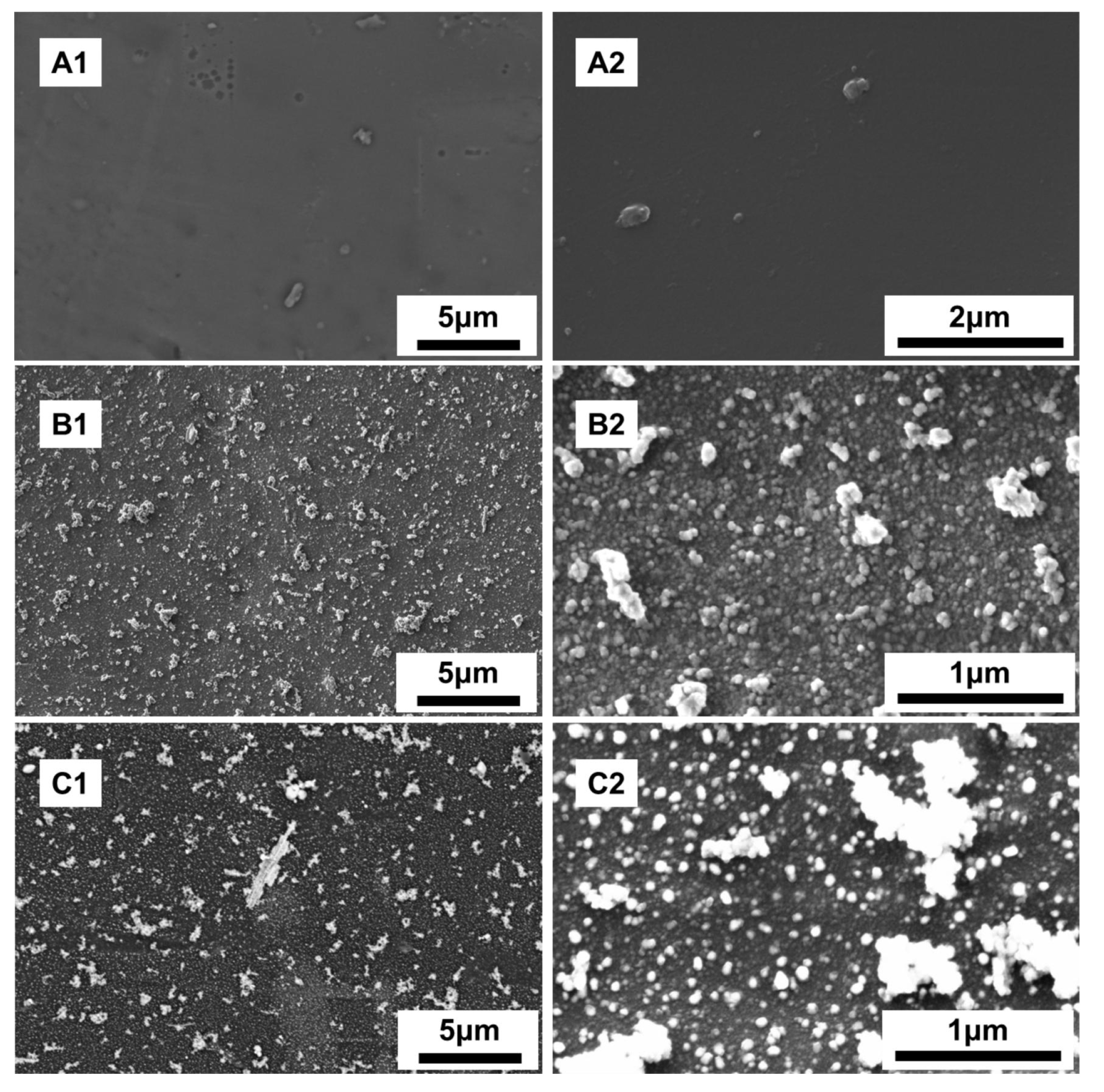
The SEM inspection of the sample surfaces during pre-treatment revealed strong changes in the microstructure, as expected from wettability results. In its initial state, the CFRP presented a flat polymeric surface, only showing small irregularities and heterogeneities, probably due to defects during the fabrication process and external pollution (see Figure 4A). Once exposed to chemical etching and a sensitization bath, a continuous layer of 30–50 nm nuclei was formed at the surface and it exhibited big micro-aggregates (Figure 4B). In addition, the activation seems to have had an effect on the previous structure by growing the micro-aggregates into bigger particles of 60–90 nm in size (Figure 4C). These observable physical changes were combined with changes in the chemical composition, as seen in the EDS spectra.
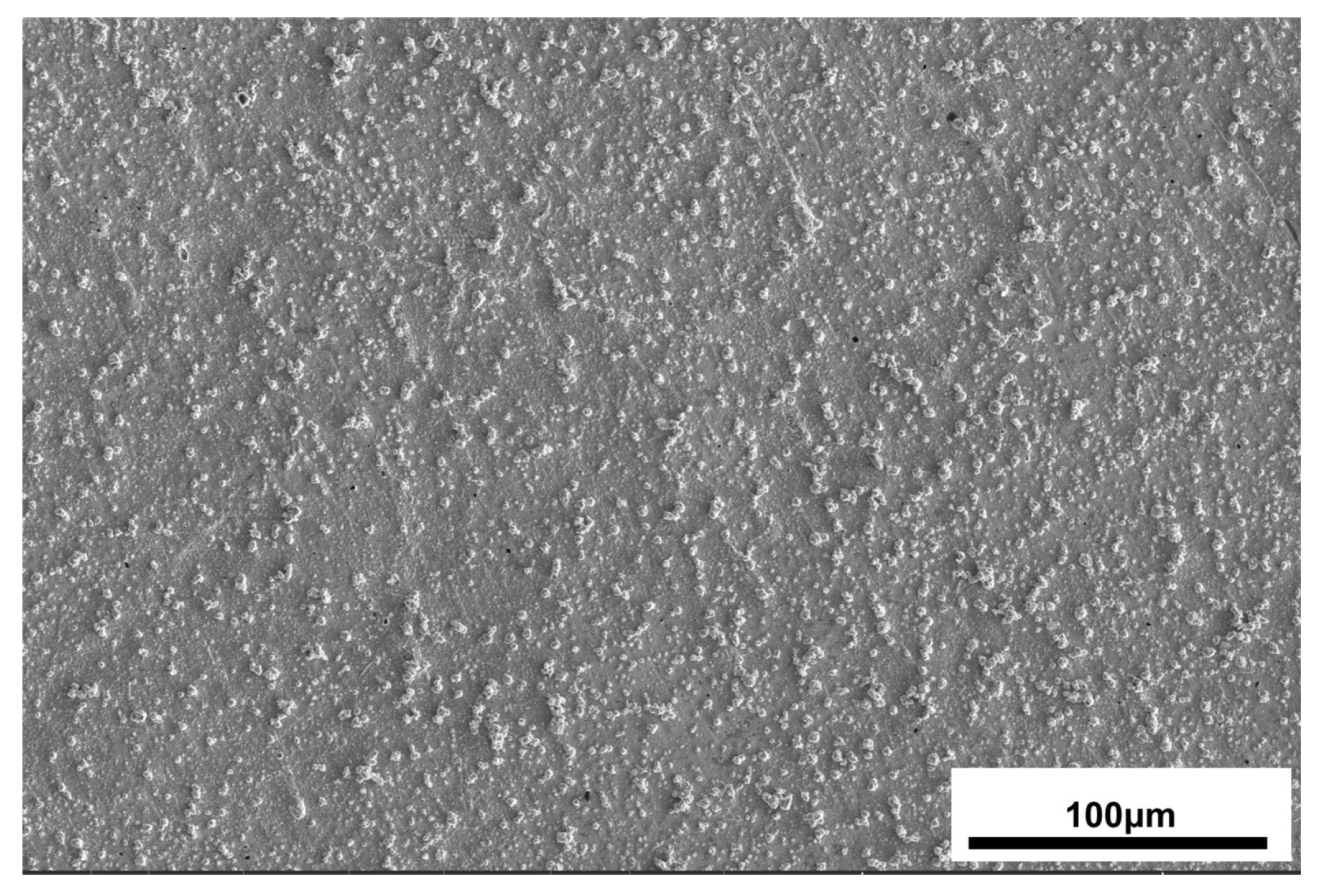
The samples that were coated with copper were also inspected under SEM to obtain more information about the morphology of the deposit. As observed at the macroscale, an uninterrupted and homogeneous layer of copper along the parts was revealed at the microscale (see Figure 5). The reduction of copper occurred extensively at the surfaces that were exposed to the bath. It could be easily observed that the structure presented a continuous layer, on top of which small copper promontories of approximately 0.5–3 μm in diameter were visible, and these created a dotted-like effect.
According to previous studies related to the formation of electroless copper layers, the deposition process follows the nucleation, growth and coalescence mechanisms. Furthermore, Paunovic [18] stated that the layer formation happens in two different stages, namely the thin film stage and the bulk stage. It was also stated in his work that during the inception of the deposition at the first stage, the predominant phenomenon is nucleation. The creation of three-dimensional crystallites at this point increases the average density in terms of number of copper nuclei. Once this number reaches a maximum, individual crystals begin the coalescence process, in which the copper grains grow laterally to form a continuous film. The quality and strength of the final coating strongly depends on how the crystallites are merged during coalescence, since a favorable orientation of the nuclei results in a lower number of defects and pores and, thus, better overall properties. Furthermore, during the bulk stage, the thickness of the film is increased by the growth of favorably oriented grains and later by the nucleation of new grains on top of the previous layer [18].
The evolution during growth of coatings was paid especial attention. Copper layer growth was carefully observed to check whether the behavior reported in literature was also reproduced in our process. A set of samples was dedicated to this study, and while their surface preparation was realized in the same conditions as the main samples, they were intentionally coated for insufficient times (under 5 min). This allowed for the obtainment of information about the early stages of the deposition process by employing SEM inspection.
Figure 6A shows the sample that was exposed to an electroless bath for barely 60–90 s. It can be easily observed that a structure of isolated cubic copper crystals began to form on the substrate. Most of these cubes were 150–200 nm in width, but smaller grains below 100 nm could be found, which means that some of the crystals were not fully developed. At this stage, nucleation was the predominant ongoing process because a significant part of the surface still lacked copper crystals. In addition, fine rounded particles were found on the dark background layer when observed in detail, which might have been be attributed to catalyst seeds that were inherited from activation or incipient copper crystals.
By contrast, it can be seen in Figure 6B that the entire surface was already covered by copper cubes only 180 s after immersion. The formation of new particles on the substrate seemed not possible anymore, and, at this point, the cubic nuclei already grew laterally such that they were now forming a continuous layer. It was observed that during their growth, the crystals eventually reached the neighbors and created some sort of interference between differently oriented grains. The coalescence of the cubic structures led to a thick layer with presence of small gaps, and, according to the process description in literature [18], the thin film stage ended. Moreover, Figure 6C shows a fully developed layer after 300 s (sample S1) in which the initial cubic structures were harder to distinguish. The base grains grew vertically but also laterally, so the gaps between them were closed or completely filled with copper. In addition, a new generation was created on top, and some of them grew selectively, forming globular structures at the surface.
The transversal cuts of sample S3 in Figure 6D show the copper layer in two different regions of the coating. The grain structure, in which domains of different orientations merged to form the layer, can be observed in the pictures. Additionally, some type of defects can be noticed in the bulk of the copper layer in form of lack of material. The presence of these voids in the deposited material could have been due to a local interruption of metal reduction. Also, trapped H2 bubbles could have promoted the void formation. Both mechanisms were observed by Nakahara et al. [19] in their study. For a better understanding of the process, one can write the reaction proposed in literature for electroless copper deposition with formaldehyde as the reducing agent [16]:
Cu2+ + 2HCHO + 4OH = Cu + 2HCOO + 2H2O + H2
As previously detailed, bubbling was observed at the sample surface during copper plating. Basically, the electron exchange between the reducing agent and the copper ions produced hydrogen gas, among other side species. The generation of H2 gas was proportional to the amount of copper reduced, and when the reaction intensified, the hydrogen production did too. It has been reported in literature that the electroless copper process exhibits two different rates of reaction from the electrochemical point of view: the induction period and the steady state. The induction period refers to the time until the anodic and cathodic reactions (HCHO oxidation and Cu2+ reduction, respectively) reach their mixed potential and begin to produce a stable reaction called the steady state [16]. Thus, hydrogen gas production increases over time, until the steady state is reached and the process remains stable.
As also reported in literature, the duration of the periods depends on several factors, such as ion concentration, temperature and pH. Indeed, when looking carefully at Equation (2), one can realize the strong influence of the pH in the chemical reaction due to the presence of the term OH in the chemical balance. In fact, the consumption of this species is the cause of the rapid decrease of pH, and it makes it necessary to frequently replenish the pH regulator during reaction.
However, Figure 6D shows a highly heterogeneous cross section with a very rough coating surface at some sites. The presence of regrowth globules on top of the copper base layer strongly affected the observed thickness of the coating. Additionally, another important source of inhomogeneity may have been lying on the high roughness of the sensitization layer, which presented undesired micrometric and sub-micrometric grains on top (see Figure 4B2). The formation of these structures could be probably avoided by a finer tune of the bath conditions such as reagent concentration, exposure time, and temperature. Additionally, either a more vigorous stirring of the fluid during sensitization or subsequent short ultrasonication cycles might cause nocuous particle detaching.
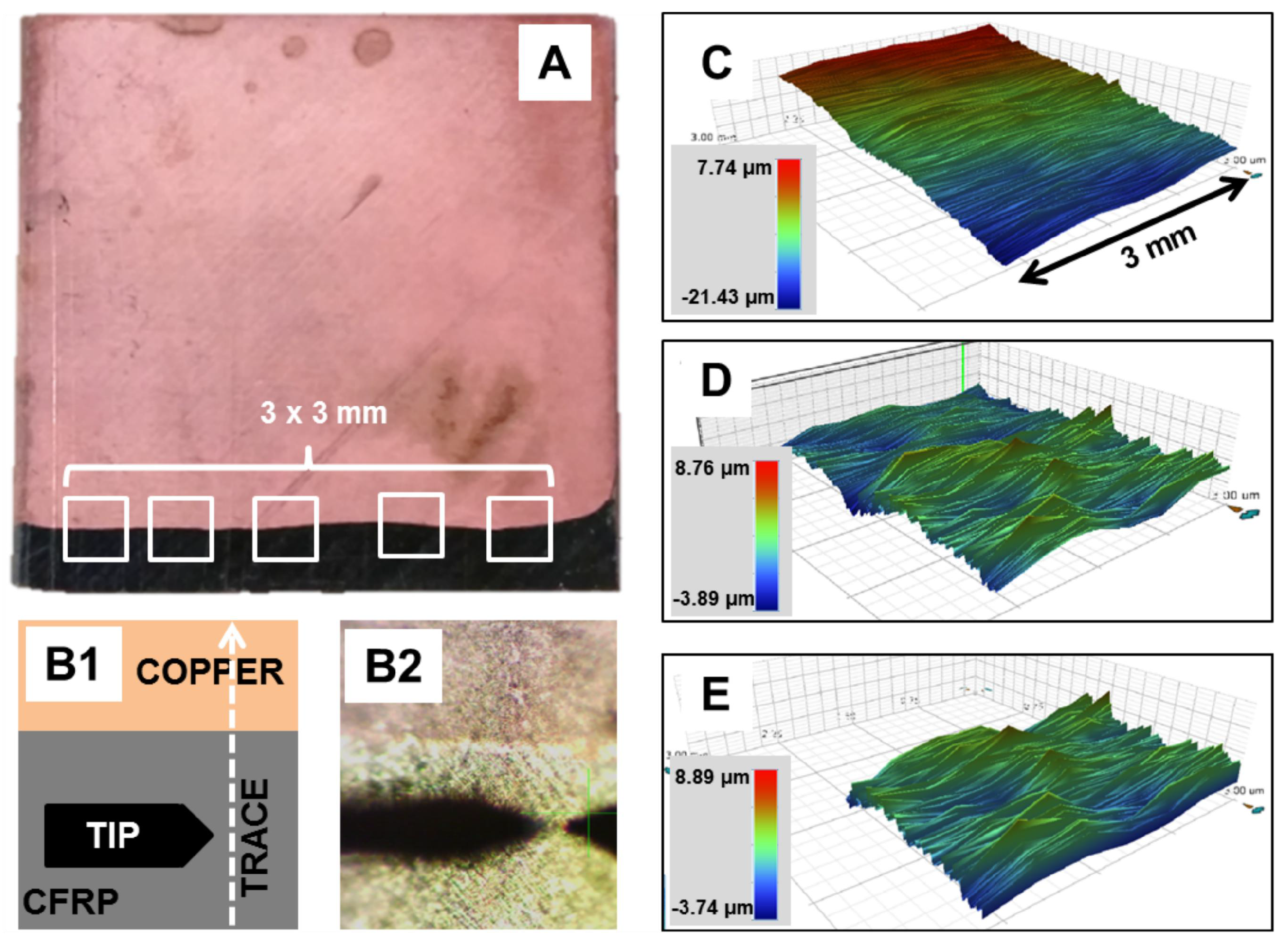
A new specific experimental method was designed in order to have reliable data of the thickness by employing the profilometry of relatively large areas.
Figure 7 shows the sequence for obtaining the layer thickness from the surface data. The process began by physically creating a sharp edge in the copper coating (Figure 7A). The samples were partially immersed in a solution of ammonium persulfate, which is a common oxidizing agent that is employed for copper etching. Copper and any other metallic species on the samples were totally removed at the immersed area. The sample was then thoroughly rinsed with water to prevent any migration of the etching solution to the boundaries of the remaining layer. After that, the samples were inspected with a profilometer (Figure 7B). Four-to-six 3 mm × 3 mm edge areas were analyzed in each sample in 15 traces with a spatial resolution of 200 µm in the traverse direction. Near 105 points in total were extracted from each area (Figure 7C). The collected data were then processed to remove the sample tilt by attending to the average level that was presented in the uncoated region (Figure 7D). After levelling, the coated region was isolated, and the height of the points was averaged by taking the average level of the uncoated composite as zero (Figure 7E).
The processed thickness data are plotted in Figure 8A. Obviously, there was a strong dependence of the thickness of coatings with the exposure to electroless bath. The layer of the 5 min samples was near 1 µm thick, and there was an uptrend showing values of 1.3 and 2 µm for 15 and 60 min, respectively. Nevertheless, the growth rate was lower for higher times, which was in accordance with the literature. Paunovic stated that at some point, the growth rate of crystals is reduced due to the higher degree of inhibition and overpotential in them [18]. The cessation of perpendicular growth is always dependent on the plating solution variables and kinetic parameters of the particular reaction. The depletion of reactants, for example, can play an important role in the growth rate and, thus, in the thickness of the final layer.
The roughness of the samples was also investigated by using the profilometer, and the data are plotted in Figure 8B. The average roughness of the coatings also increased with the time of deposition. The initial value of the as-manufactured CFRP was 0.81 µm of surface roughness (Ra), and this was the minimum roughness observed. After only 5 min of electroless deposition, the Ra already reached about 1.33 µm, whereas for 15 min, it became 1.55 µm. The highest Ra that was observed was 2.17 µm for the 60 min plated samples. Again, a non-linear rate in the increasing trend of this parameter could be seen, as with the copper thickness. As previously noticed in SEM micrographs, the formation of regrowth grains on top of the coalesced crystals layer can have an important role in the average roughness. These particles have been observed to be bigger at higher times of deposition, and the surface texture is accordingly affected.

3.2. Physical Properties of the Coatings

The samples were also subjected to laboratory testing to know the performances that were achieved by the copper coatings. More specifically, the quality of the copper layers that were deposited was analyzed from the electrical point of view, since the main driver of the work was to increase the surface conductivity of the parts. Moreover, another aspect of the coatings to take into account was the resistance to separation of the layers, because poorly adhered coatings would present frequent detachment and flaking, which might ruin whatever advantages obtained in an electrical feature. On the other hand, since composite materials are very often exposed to certain products, an analysis on the resistance to some of the most frequent aviation contaminants was conducted.

3.2.1. Electrical Performance

Very often, the electrical performance of thin metal layers is assessed by sheet resistance measurements. Sheet resistance is expressed in [Ω/□] and is useful when characterizing thin conductor layers because it is an invariant property of coatings, regardless of the lateral dimensions of the measured part. As previously seen in Equation (1), a geometric correction factor (C) must be applied if the measuring conditions are not ideal. For instance, if the surface to be measured presents a lateral size smaller than 40 times the characteristic distance of the probe pins, it is considered that the measurement is affected by the proximity of the edges. Studies have been carried out on this topic, and numeric tables of correction factors can be found depending on the particular cases of the relation between the thickness, length, or width of the layer, as well as the probe characteristic distance [15].
The sheet resistance of the samples is presented in Figure 9. The results show a downtrend in the average values with the time of plating. Longer times of exposure to the copper electroless solution produced better performing layers. The samples coated for 5 min presented 385 mΩ/□ which is the highest sheet resistance, whereas the samples that were coated for 15 min exhibited a significant drop of this value to near 95 mΩ/□. After 60 min of reaction, the samples presented a resistance of 58 mΩ/□, which was the lowest. The strong drop in this characteristic between 5 and 15 min of plating could be attributed to the full coalescence of the isolated copper nuclei within this period, thereby significantly improving the electrical performance of the coating due to the new electrical paths that were created. During the period between 15 and 60 min, the decrease in the sheet resistance was lesser than in the previous one, which means that the electrical improvement after the formation of the continuous layer was low.
In addition, when paying attention to the standard deviation bars of the sheet resistance plot, one can see that there was a very high dispersion of the data in the 5 min samples. This might be attributable to heterogeneities in the copper layer at its first stage. According to Paunovic [18], the recently added HCHO starts its conversion into electroactive species at the beginning of the reaction by a cascade of intermediate sub-reactions. The sequence of conversion is strongly dependent on the pH and the temperature, so slight changes in these parameters in the bulk of the solution could lead to local acceleration–deceleration phenomena. All these effects may cause an inhomogeneous copper growth with local discontinuities in the layer, and then significant difference can be found in the electrical measurements. Nevertheless, the values that can be observed in the graph are in accordance with that of previous studies such as that of Sha et al. [20], in which the electrolessly deposited copper layers that employed formaldehyde as a reducing agent exhibited a sheet resistances ranging from 10–100 mΩ/□.
The resistivity of the coatings was also evaluated and compared with that of bulk copper. This characteristic of metal deposits provides information about the quality of the coating because it is strongly affected by the presence of defects. Electrical resistivity could be calculated by the mathematical relationship involving sheet resistance and thickness.
Rsq = ρ/t
where ρ = resistivity; t = thickness.
Equation (3) only applies to thin films and helps in the understanding how resistivity and sheet resistance can be related via the thickness of the layer; the results are plotted in Figure 9. The electroless copper layer showed a resistivity near 40 µΩ·cm for the lowest coating time, whereas a significant drop of the values to near 12 µΩ·cm could be noticed for the 15 min samples. There was almost no change in this property for the 60 min samples, and the calculated resistivity remained at the same value. The structure of the layer, which was strongly affected by the packing of the crystals, seemed to be similar for the coatings after 15 min.
The resistivity that was measured on our coatings was far from the values of bulk copper, which is approximately 1.7 µΩ·cm [20]. The large difference between the theoretical value and that of our coatings was most likely related to all the mechanisms that could have introduced defects into the coating, such as the incorporation of impurities, voids, dislocations, and stress between grains, all of which were mentioned in Paunovic’s work [18]. Additionally, the unavoidable variability in the thicknesses measurement could have brought strong variations in the values of resistivity. Nevertheless, according to Sha et al., some other chemistry-related parameters, such as the reducing agent concentration in the baths, can play important roles in the final coating resistivity. In particular, they can lead to the presence of diamond shaped crystals with a small size, which significantly increases the grain boundaries and the amount of voids, regardless the degree of twinning, thus forming more resistive coatings [20]. According to the layer formation study (see Section 3.1), these kind of structures were observed in the first stages of the layer growth. More specifically, the initial layer of copper was composed of 200 nm-width cubic crystals, very similar to that described by Sha et al. in their resistivity-to-porosity ratio investigation. On the other hand, following the initial stage, the twinned cubic crystals layer was covered by a dense layer of copper that seemed to be filling up (or at least closing) the upper gaps between the cubes.

3.2.2. Cross-Cut Test

An obviously important characteristic of coatings is the quality of their adhesion to the substrate. The strength of attachment of the copper layer to the composite is of great interest since it can give idea of the quality of the process, especially the surface preparation. Normally, the adhesion of a coating to the substrate is considered to occur by two means. Firstly, the layer is mechanically anchored at the microscale to the peaks and valleys of the part, which has been previously treated to increase its specific surface as well as the micro-roughness. The greater the contact surface and the higher the micro-roughness, the better the mechanical coupling of the deposited material. Secondly, the chemical bonds and electrostatic forces between the coating and the substrate are believed the most empowering reasons for the adhesion and produce the strongest attachments [21].
The relevant standard [22] established six different classifications that depend of the percentage of coating detached from 0 (no detachment at all) to 5 (a detachment greater than 65% of the area), with intermediate levels. It is important to remark that this is not an adhesion test, but a resistance to separation test, to which the adhesion between the layer and the substrate, among other features of the coating, partially contributes.
After the cuts, the affected area was cleaned of debris with a soft brush and then compared with the visual references included in the standard [22]. The results are shown in Table 2, and Figure 10 shows actual magnified images of the tested areas. The grooves that were created reached the substrate, and the detachment that was observed on all the coatings was null or very small.
The copper layer presented sharp edges at the cuts, and no flaking was observed. It could be seen that there was no noticeable degradation of the present material, and it remained fully attached to the substrate. This behavior demonstrated a very good resistance to the separation of the coatings, and, thus, all of them were classified as a rating of 0 according to the standard. Such behavior could be attributed to an efficient pre-treatment of the substrate in combination with strong bonding between the metal layer and the activation layer. A high resistance to separation is important for functional coatings that are applied to composites because protective coatings or aesthetic finishing are normally applied on top. The performance of these materials, such as primers, paints, varnishes, or gel-coats, strongly depends on a good anchorage, and, thus, an easily detachable coating is not acceptable.

3.2.3. Resistance to Contaminants

Aeronautic materials are very often exposed to solvents and other contaminants that are present in the manufacturing facilities. In the case of coatings for CFRP parts in aviation such as paints and primers, they are usually in contact with organic solvents, greases, and hydrocarbons. This type of substance may have a persistent effect on the applied layers, and several problems that are derived from the degradation of the material, such as local lack of protection of the substrate, a loss of properties, and long-term detachment, can arise [23]. Thus, it is relevant to study the effect of these possible contaminants.
Copper is extremely sensitive to oxidizing substances and to some well-known acids. Nitric acid or concentrated sulfuric acid will completely and rapidly dissolve the copper layer. However, some other substances such as solvents may have different interactions, such as long-term degradation. In order to evaluate the coating’s sensitiveness, a year-term experiment was conducted by immersing electrolessly-coated CFRP parts into common fluids that are often in contact with surfaces in aviation. Methyl-ethyl ketone (MEK) and acetone, which are widely used products for cleaning and degreasing, were used for the experiment. Additionally, aviation kerosene and de-icing fluids are very often in contact with aircraft surfaces. The samples were kept immersed in the fluids inside polyethylene sealed bottles at room temperature, with periodic checks being carried out, and then the coated CFRP specimens and remaining solvents were visually inspected after one year.
Table 3 shows the results of the exposure of the copper electroless coatings to the abovementioned products. The layer was quickly erased when exposed to MEK. The coating was removed within the first hours, and in the same way, the solvent began acquiring the typical blueish tone of dissolved copper ions. The sample extraction revealed that no metallic copper remained attached to the surface. A similar behavior was found after exposure to acetone, though this occurred at a slower rate of degradation. The coating seemed unaffected by the solvent for several days, but it suffered a severe long-term degradation that removed a whole layer from the surface. On the other hand, the de-icing fluid had very little effect on the coating. After one year of immersion, the coating was visually unaltered, and the sample presented very tiny detachments in visibly swollen areas. However, the fluid remained stable in color and transparency. A possible explanation for this is that the product had flown through the pores and defects of the copper deposit, reaching the interlayer space and thus swelling the coating, which could have promoted the detachment in particular locations. Furthermore, tiny metallic copper flakes were found at the bottom of the flask, which meant that there was no chemical attack of the metal—only a mechanical detachment effect. Aviation fuel, by contrast, generally degraded the coating, which presented a significant change in color. A discrete detachment of small millimeter-sized areas occurred at many locations along the surface. In addition, a dark deposit was observed at the bottom of the plastic container, and this was attributed to the chemical degradation or oxidation of the metallic layer.

4. Conclusions

During this study, a thin layer of copper was successfully deposited on epoxy-based CFRP samples by employing an electroless deposition process with the aim of increasing the electrical performance of the parts. A batch of 40 mm × 40 mm samples was extracted from a panel that was manufactured by prepreg automatic tape lay-up and a subsequent autoclaving process. Furthermore, for metallization, a set of self-designed baths was produced with cheap and readily available reagents, and the deposition process was held by using very common laboratory equipment. The samples were subjected to four-stage pre-treatment including cleaning, chemical etching, sensitization, and activation. After that, the parts were immersed into an electroless bath for 5, 15, and 60 min, rinsed in de-ionized water, and dried. The coatings that were produced were subjected to investigation, and their properties were analyzed.
Changes in the microstructure of the sample surface were observed by SEM and EDS after each pre-treatment step, such as the formation of a globular catalytic surface at the end of the process. The copper deposits presented an increasing average thickness with deposition time, ranging from near 1 µm, achieved at 5 min, to near 2 µm at 60 min. The roughness of the coatings also showed an increasing trend with the time of reaction, and Ra values from 1.33 to 2.17 µm were observed. A deeper investigation of the copper crystals growth stage revealed the initial formation of 200 nm cubic structures during the first minutes of reaction, followed by the coalescence of the grains and a further nucleation of new globular particles on top, ranging from 1 to 4 µm in diameter. The sheet resistance values that were observed for 5 min of deposition were slightly below 400 mΩ/□ on average, with a high dispersion of the measurements. Heterogeneities at the initial stage of the reaction could have led to discontinuities in the coatings and thus to highly variable measurements. This effect was mitigated at longer times, and the thicker coatings were better performing layers, presenting 95 and 58 mΩ/□ at 15 and 60 min, respectively. In addition, the resistivity measurements led us to think that the thicker coatings presented better quality in terms of defects, porosity, and inclusions. Cross-cut tests showed that the coatings were properly adhered to the substrate, and a rating of 0, according to ISO 2409, was observed for all of them, meaning that no detachment occurred. Furthermore, the sensitiveness of the coatings to usual aviation contaminants was evaluated. After one year of exposure of the coatings to different fluids, it was found that the electroless copper layers were dissolved by MEK, acetone, and kerosene, but they remained chemically unaltered by de-icing fluid.
The suitability of electroless copper coatings for enhancing the electrical conductivity of CFRP materials was successfully proved during this work. The metal layers that were produced by employing this well-known technique presented promising properties, making electroless deposition a good strategy to take into account when increasing the electrical features of such materials.

Author Contributions

Conceptualization, S.d.J., E.G. and A.J.-M.; methodology, S.d.J.; validation, E.G., A.J.-M. and F.S.; formal analysis, S.d.J.; investigation, S.d.J.; resources, S.d.J., E.G., A.J.-M. and F.S.; data curation, S.d.J.; writing—original draft preparation, S.d.J.; writing—review and editing, S.d.J., E.G., A.J.-M. and F.S.; visualization, S.d.J.; supervision, E.G. and A.J.-M.; All authors have read and agreed to the published version of the manuscript.

Funding

This research received no external funding.

Conflicts of Interest

The authors declare no conflict of interest.

References

  1. Soutis, C. Carbon fiber reinforced plastics in aircraft construction. Mater. Sci. Eng. A 2005, 412, 171–176. [Google Scholar] [CrossRef]
  2. Ghobadi, A. Common type of damages in composites and their inspections. World J. Mech. 2017, 7, 24–33. [Google Scholar] [CrossRef] [Green Version]
  3. Karch, C.; Metzner, C. Lightning protection of carbon fibre reinforced plastics—An Overview. In Proceedings of the 2016 33rd International Conference on Lightning Protection, Estoril, Portugal, 25–30 September 2016. [Google Scholar] [CrossRef]
  4. Zhou, X.L.; Chen, A.F.; Liu, J.C.; Wu, X.K.; Zhang, J.S. Preparation of metallic coatings on polymer matrix composites by cold spray. Surf. Coatings Technol. 2011, 206, 132–136. [Google Scholar] [CrossRef]
  5. Gou, J.; Tang, Y.; Liang, F.; Zhao, Z.; Firsich, D.; Fielding, J. Carbon nanofiber paper for lightning strike protection of composite materials. Compos. Part B Eng. 2010, 41, 192–198. [Google Scholar] [CrossRef]
  6. Han, J.H.; Zhang, H.; Chen, M.J.; Wang, D.; Liu, Q.; Wu, Q.L.; Zhang, Z. The combination of carbon nanotube buckypaper and insulating adhesive for lightning strike protection of the carbon fiber/epoxy laminates. Carbon 2015, 94, 101–113. [Google Scholar] [CrossRef]
  7. Décor Engineering, Aeronautics. 2018. Available online: www.decorengineering.com.au/aeronautics (accessed on 4 March 2020).
  8. Gan, Y.X.; Chen, C.O.; Li, C.G. Preparation of metal-coated carbon fiber reinforced composites and their electromagnetic properties. Mater. Manuf. Process. 1994, 9, 249–262. [Google Scholar] [CrossRef]
  9. Dubin, V.M.; Shacham-Diamand, Y.; Ting, C.H.; Zhao, B.; Vasudev, P.K. Electroless Cu Deposition on a Barrier Layer by Cu Contact Displacement for ULSI Applications. U.S. Patent 5,891,513, 6 April 1999. [Google Scholar]
  10. Burri, F.; Fertl, M.; Feusi, P.; Henneck, R.; Kirch, K.; Lauss, B.; Rüttimann, P.; Schmidt-Wellenburg, P.; Schnabel, A.; Voigt, J.; et al. Copper coated carbon fiber reinforced plastics for high and ultra high vacuum applications. Vacuum 2014, 101, 212–216. [Google Scholar] [CrossRef] [Green Version]
  11. Geterud, E.G.; Bergmark, P.; Yang, J. Lightweight waveguide and antenna components using plating on plastics. In Proceedings of the 2013 7th European Conference on Antennas and Propagation (EuCAP), Gothenburg, Sweden, 8–12 April 2013; pp. 1812–1815. [Google Scholar]
  12. Louis, M.; Joshi, S.P.; Brockmann, W. An experimental investigation of through-thickness electrical resistivity of CFRP laminates. Compos. Sci. Technol. 2001, 61, 911–919. [Google Scholar] [CrossRef]
  13. Kuzmik, J.J. Plating on plastics. In Applications Electroless Plating—Fundmentals Applications; William Andrew: Norwich, NY, USA, 1990; pp. 377–399. [Google Scholar]
  14. Ossila Ltd. Sheet Resistance: A Guide to Theory. Available online: www.ossila.com/pages/sheet-resistance-theory#measuring-sheet-resistance (accessed on 4 March 2020).
  15. Topsoe, H. Geometric factors in four point probe resistivity measurement. Bulletin 1968, 472, 63. [Google Scholar]
  16. Djokić, S.S. Electroless deposition of metals and alloys. In Modern Aspects of Electrochemistry; Springer: Boston, MA, USA, 2002; pp. 51–113. [Google Scholar]
  17. Yasuda, T.; Okuno, T.; Yasuda, H. Contact angle of water on polymer surfaces. Langmuir 1994, 10, 2435–2439. [Google Scholar] [CrossRef]
  18. Paunovic, M. Electroless Deposition of Copper, Modern Electroplating, 5th ed.; John Willey & Sons, Inc.: Hoboken, NJ, USA, 2010; Volume 1, pp. 433–446. [Google Scholar] [CrossRef]
  19. Nakahara, S.; Okinaka, Y. Microstructure and ductility of electroless copper deposits. Acta Metall. 1983, 31, 713–724. [Google Scholar] [CrossRef]
  20. Sha, W.; Wu, X.; Keong, K.G. Electroless Copper and Nickel-Phosphorus Plating: Processing, Characterisation and Modelling; Elsevier: Amsterdam, The Netherlands, 2011. [Google Scholar]
  21. Awaja, F.; Gilbert, M.; Kelly, G.; Fox, B.; Pigram, P.J. Adhesion of polymers. Prog. Polym. Sci. 2009, 34, 948–968. [Google Scholar] [CrossRef]
  22. ISO 2409—Paints and Varnishes: Cross-Cut Test; ISO: Geneva, Switzerland, 2013.
  23. Stenzel, V.; Wilke, Y.; Hage, W. Drag-reducing paints for the reduction of fuel consumption in aviation and shipping. Prog. Org. Coatings. 2011, 70, 224–229. [Google Scholar] [CrossRef]
Figure 1. Electroless copper-coated samples. (A) Tooling side; (B) vacuum bag side.
Coatings 10 00271 g001
Figure 2. (a) Illustration of the proposed evolution of the species at the surface. (b) EDS spectra of the surface after pre-treatment stages: (A) chemical etch, (B) sensitization, and (C) activation.
Coatings 10 00271 g002
Figure 3. Water droplet contact angle measurements after pretreatment stages. REF: untreated surface; ETCH: after chemical etching; SENS: after sensitization; and ACT: after activation.
Coatings 10 00271 g003
Figure 4. SEM images of the sample surface: (A1) initial, (A2) initial at higher magnification; (B1) after sensitization, (B2) detail of the magnified tin structures; (C1) after activation, and (C2) detail of the silver deposit.
Coatings 10 00271 g004
Figure 5. SEM image of copper-coated carbon fiber-reinforced polymer (CFRP) for 60 min.
Coatings 10 00271 g005
Figure 6. (AC) SEM micrographs showing the different growing stages. Times after immersion were of 90, 180 and 300 s respectively. The cubic structures of the incipient copper crystals are visible in (A,B). (D) is the cross section of the S3 sample (60 min) coatings at two different locations. SEM pictures were taken with the hybrid backscattered/secondary electron mode of detection.
Coatings 10 00271 g006
Figure 7. Thickness evaluation process by profilometry. (A) Preparation of sharp edges on the coatings; (B1) schematic representation of the profile acquisition, (B2) actual snapshot of the process; (C) 3D view of the extracted data; (D) flattened data; and (E) masked area for average thickness evaluation.
Coatings 10 00271 g007
Figure 8. (A) Thickness measurements that were obtained by profilometry; (B) average roughness of the samples.
Coatings 10 00271 g008
Figure 9. Sheet resistance and coating resistivity of the 40 mm × 40 mm samples.
Coatings 10 00271 g009
Figure 10. Cross-cut test micrographs: (A) low magnification of S1 sample cut area; (B) high magnification of S3 cuts intersection. For clarification, the horizontal straight mark from left to right in (A) arose from a defect on the manufacturing tooling, and it extended across the whole sample width.
Coatings 10 00271 g010
Table 1. Immersion times of the samples in an electroless plating bath.
SampleTime (min)
S15
S215
S360
Table 2. Cross-cut test classifications according to ISO 2409.
SampleISO 2409 Rating
S10
S20
S30
Table 3. Degradation behavior of copper electroless coatings that were exposed to several products.
ContaminantHabitual UseVisible DegradationDegradation RateObservations
Methyl-ethyl ketoneCleaning and degreasingTotalImmediateNo copper left on the surface. Remaining solvent colored blue.
AcetoneCleaning and degreasingTotalVery slowNo copper left on the surface. Remaining solvent colored blue.
NYCO 8243De-icing of surfacesLightSlowFew small areas of copper layer are detached. No color change of the solvent.
Aviation keroseneFuelModerateQuickChange in color of the coating. General detachment of small areas the layer. A black precipitate remained at the bottom of the container.
Methyl-ethyl ketoneCleaning and degreasingTotalImmediateNo copper left on the surface. Remaining solvent colored blue.

