Article

Laser Shock Induced Deformation of Copper Foil on Diverse Molds and the Cross-Sectional Microstructure Changes

College of Mechanical & Electrical Engineering, China University of Mining & Technology, Xuzhou 221116, China
*
Author to whom correspondence should be addressed.
Coatings 2020, 10(12), 1264; https://doi.org/10.3390/coatings10121264
Submission received: 5 November 2020 / Revised: 10 December 2020 / Accepted: 15 December 2020 / Published: 21 December 2020
(This article belongs to the Section Surface Characterization, Deposition and Modification)

Abstract

:
The microscale structures prepared on copper foil by laser shock deformation was introduced in the paper. The various sizes of hexagonal structures were successfully fabricated on copper foil with different molds. The influence of laser energy on the deformation depth of a hexagonal structure was studied using experiments. The morphology of the hexagonal structures on copper foil was observed by a three-dimensional profilometer, and mechanical property were characterized by a nanoindenter. A finite element model was established in order to describe the copper foil forming mechanism on mold and calculate the residual stress distribution. The microstructures and cross-section deformation of copper foil on different molds were also observed. The results indicated that the depth of hexagonal structures on 50# mold was higher than that of the structures on 100# mold and 230# mold, and the depth of hexagonal structures increased with the increasing of pulse laser energy. The copper foil above the mold hexagon side was bent and thinned after laser shock, and the grains of copper foil were also refining. The mechanical properties of copper foil were improved after laser shock was performed on the mold.

1. Introduction

Laser shock forming was an ultrafast forming technology that has been widely used in microelectromechanical systems (MEMS) and microactuator manufacturing [1,2,3]. From nanoscale to millimeter scale, textures can be fabricated on metal or nonmetal surfaces by laser shock [4,5]. Because of the great application of laser shock in material forming, many scholars have carried out relevant research in this area.
To investigate the size effect on deformation behavior in laser shock forming, Liu et al. designed various micromolds and laser parameters to reveal the forming mechanism by annealed copper foils with different grain sizes [6]. Zheng et al. studied the effect of confining overlay on shock deformation in a microscale laser shock process by experimental means, and the appropriate confining layer thickness and material were obtained [7]. The deformation angle, deformation depth, precision, thickness thinning ratio, and surface quality of laser-shocked aluminum foil was studied to characterize the forming properties in laser dynamic flexible forming [8]. Ehrhardt et al. fabricated submicrometer-scaled structures on solid copper by laser embossing, and they investigated different laser energies and residual stress on the patterned surface [9]. Cheng et al. carried out the scalable patterning on NiTi shape memory alloy by laser shock direct imprinting, and they demonstrated that thermally controllable surface pattern can be generated on NiTi surface by laser shock [10]. Xiong et al. introduced a temperature-assisted laser shock imprinting technique to fabricate large-area microstructures on metal foil. The effect of temperature on the plasticity, flow stress, dynamic yield strength, and deformation resilience in laser shock forming was calculated by a FEM, which indicated that the warm laser shock imprinting improved the forming depth, accuracy, high temperature stability, and residual stress distribution [11]. Because of the micropatterns’ property of pure titanium in biomedical applications, Shen et al. fabricated micropatterns by laser peening on pure titanium to improve its mechanical strength, and the cell culture tests on the micropatterned surface were also conducted to study its biomedical performance [12]. Wang et al. investigated laser shock microforming copper foil using a mask and flexible pad; they obtained high quality surface morphology, and the thickness distribution of copper foil was analyzed [13]. The laser shock forming of commercially pure copper and titanium sheet was studied by experimental and numerical methods. Titanium with a thickness of 13 μm was completely cut along the inner edge of micromolds at a pulse energy of 1.55 J, and the laser-driven flyer technique could achieve blanking forming [14]. Laser shock forming has proven to be an effective and scalable approach in fabricating a nanoscale hole array on graphene film [15]. A new laser shock with preshock was proposed to fabricate ultrasmooth microtextures on metallic foil, and it was found that the hardness and roughness of the texture were improved after laser shock [16]. Nagarajan et al. studied the plastic deformation on metallic foils by flexible-pad laser shock forming, which controlled the deformation pressure, and the thickness distribution of the cross section was analyzed by experimental methods [17].
In view of the current laser shock forming research, the effect of mold size and the change of microstructure in shocked material cross sections have rarely been reported. In this paper, we carry out laser shock forming of copper foil on hexagonal molds with different sizes. The 3D morphology and hardness of hexagonal structures were measured to characterize the forming results. The stress distribution, cross-section thickness, and microstructures of laser-shocked copper foil were studied, all of which reveal the forming mechanism of copper foil in the laser shock process.

2. Experimental Details

2.1. Material Preparation and Principle

Pure copper foil (Bling Co., Ltd., Taizhou, China) with a thickness of 30 μm (length: 5 mm, width: 5 mm) was used in the laser shock deformation experiments. The laser shock experiments was carried out by a Q-switched Nd:YAG pulse laser (Ziyu laser Co., Ltd., Anshan, China) with a wavelength of 1064 nm and a pulse frequency of 5 Hz, and the laser beam spot and pulse duration was 1 mm and 15 ns, respectively. In the laser shock process, a quartz glass with a thickness of 3 mm was selected as the confining layer, and the absorbing layer was black aluminum foil with a thickness of 35 μm. The molds were the 50#, 100#, and 230# transmission electron microscope copper grid (diameter: 3 mm, Zhongjingkeyi Co., Ltd., Beijing, China). The schematic of laser-shocked copper foil deformation is presented in Figure 1a. The confining layer, absorbing layer, copper foil, and TEM mold were orderly placed on a work platform (45# steel); the laser shock scanning on copper foil was achieved by a moving work platform. A self-made fixture clamped down all layers and sample, and then they were fixed on the work platform. Each layer and sample were put into the fixture, and then a confining layer was pressed with screw bolts to ensure close contact between the layers. The overlap ratio of the neighboring laser shock spot in the different samples was 0.4.
The pulse laser passed through the confining layer and burned the absorbing layer, which induced a high peak pressure shock wave at the copper foil top surface. Black aluminum foil with a thickness of 35 μm was selected as the absorbing layer to prevent the copper foil from ablation. Under the effect of pulse laser induced pressure shock wave, the copper foil generated plastic deformation with a ultrahigh strain rate, and the mold would imprint microstructures on the copper foil’s bottom surface. Fabbro et al. [18] conducted research on plasma explosion induced shock wave, and they deduced the relationship between peak pressure and laser power density. The peak pressure of laser shock wave can be described as the following formula:
P = 0.01 α 2 α + 3 × Z × I 0
where α is the efficiency of laser energy conversion to heat energy, and Z is the impedance of the confining layer and copper foil. The laser power density I0 can be calculated by Formula (2):
I 0 = 4 E π τ D 2
where τ is the pulse laser duration (15 ns), and E and D are the laser energy and beam diameter, respectively.

2.2. Experimental Apparatuses

The laser-shocked copper foils in the experiments were investigated by different measuring instruments. The morphology of laser-shocked copper foil was characterized by a three-dimensional profilometer (VHX-2000, Keyence, Osaka, Japan) and an optical microscope (GX71, OLYMPUS, Tokyo, Japan). The cross section of the copper foil was obtained by electrical discharge machining (DK7740, Shenweishukong, Co., Ltd., Suzhou, China), and then embedded into a square epoxy block. The cross-section images and microstructures of laser-shocked copper foil were observed by an optical microscope (GX71, OLYMPUS, Tokyo, Japan). After being embedded in epoxy resin, the cross section of shocked copper foil was ground with different sandpapers (600#, 1200#, 2000# in turns), and then the copper foil section was polished with a 1.5 W polishing paste (6000#). There are no scratches on the laser-shocked copper foil’s cross section in the nanoindentation tests. The square epoxy block was fixed at the work platform of the nanoindenter. The nanohardness and load-displacement curve of the copper foil were also obtained by the nanoindenter (G200, Keysight, Santa Rosa, CA, USA).

3. Results and Discussion

3.1. The Morphological Analysis of Copper Foil Deformation after Laser Shock

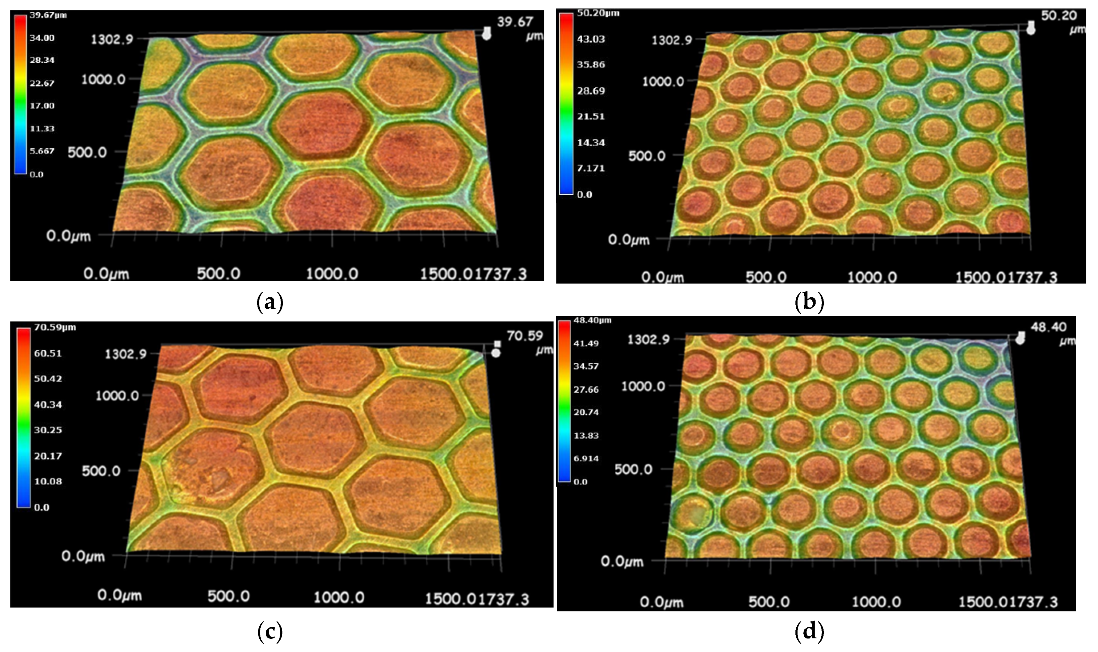
The morphology and deformation depth of the copper foil generated great changes after laser shock. In order to investigate the influence of laser energy on copper foil deformation, the copper foil samples were fabricated by different laser shock energies (0.3, 0.45, 0.6, and 0.8 J). Figure 2 shows the morphology of microstructures on the copper foil at a pulse laser energy of 0.45 and 0.8 J. It was found that the hexagonal structures on mold were successfully transferred to the copper foil surface, and the surface structures were uniform and regular. Figure 2a,c shows that the angle of the hexagonal structures was clear and the precise, and the depth of the hexagonal structures in Figure 2c is higher than that in Figure 2a. Figure 2b,d shows the morphology of laser-shocked copper foil above the 100# mold at laser energy of 0.45 and 0.8 J. The hexagonal structures of the 100# mold were manufactured on copper foil after the laser shock, but the hexagonal structures on the copper foil was somewhat circular. Compared to the hexagonal structures transferred from the 50# mold, the depth of hexagonal structures transferred from the 100# mold was smaller, and the uniformity and manufacture precision were not satisfactory.
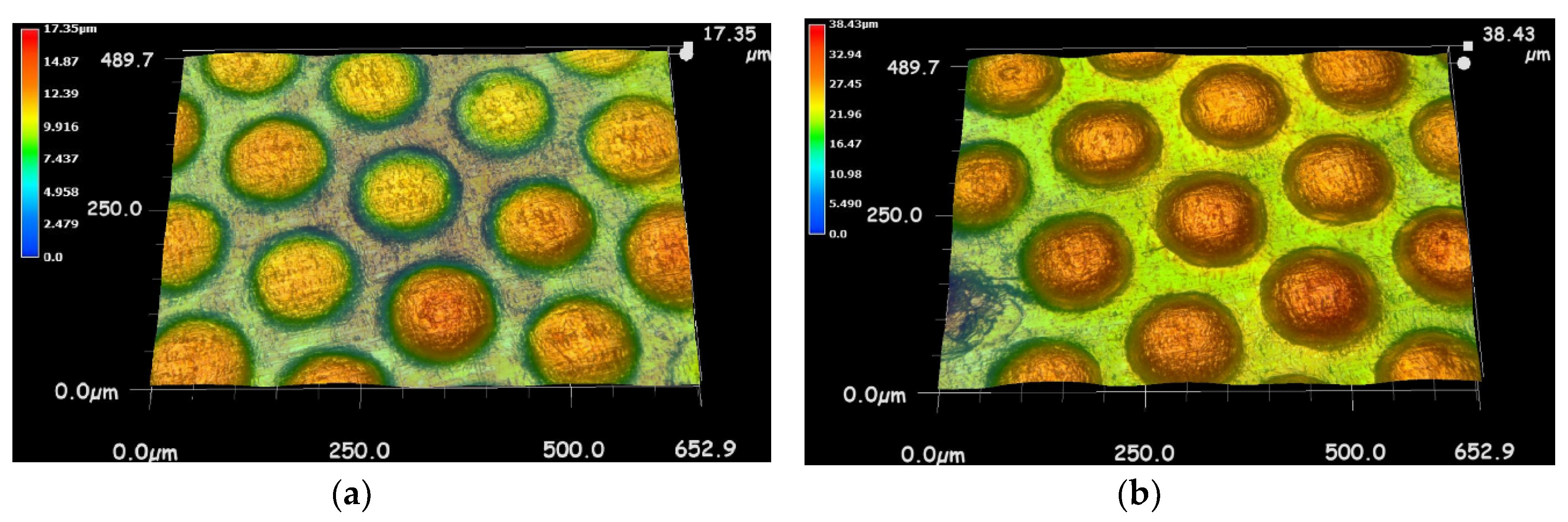
Figure 3 shows the morphology of the copper foil transferred from the 230# mold with a pulse laser energy of 0.45 and 0.8 J. The copper foil’s bottom surface formed uniform microstructures, but the hexagonal structures have almost become circular bulges. The sides and angles of the hexagonal structures disappeared after the laser shock. Compared to the morphology of the hexagonal structures on the copper foil fabricated from the 50# and 100# molds, the depth of hexagonal structures on the copper foil here was obviously reduced under the same laser energy.
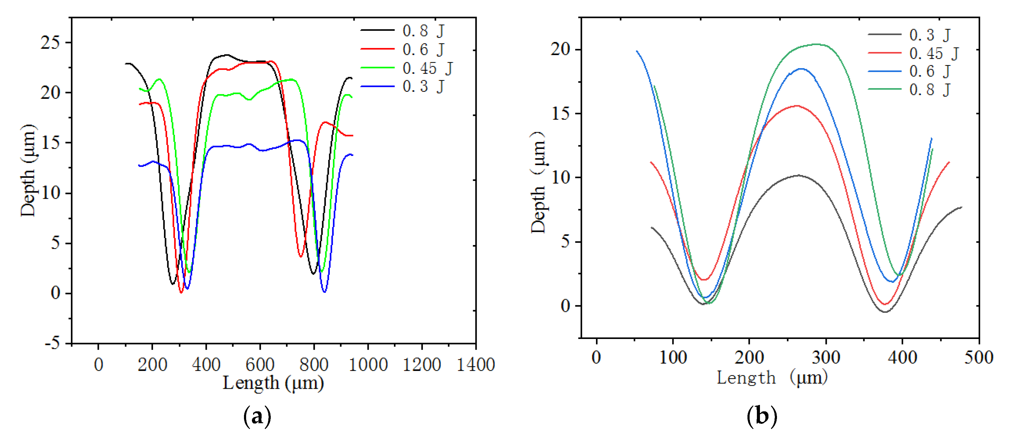
To further study the relationship between deformation depth and laser energy, the hexagonal structure profile curves fabricated on copper foil with different laser energies are given in Figure 4. The profile depth of the hexagonal structures is only about 13 μm at a laser energy of 0.3 J. The profile depth of the hexagonal structures increases with the increasing of laser energy (transferred from the 50# mold). The hexagonal structures on the copper foil surface has a maximum depth (24 μm) at a laser energy of 0.8 J. The width of the hexagonal structures fabricated from 50# mold is about 430 μm. In Figure 4b, with the increasing of laser energy, the shocked copper foil generated plastic deformation. The deformation depth of the hexagonal structure transferred from 100# mold is 10 μm at laser energy of 0.3 J. The width of the hexagonal structure fabricated from 100# mold is about 230 μm. In Figure 4c, the hexagonal structure has a minimal profile depth (8 μm) at a laser energy of 0.3 J. The width of the hexagonal structure fabricated from the 230# mold is about 160 μm. The copper foil produced maximal plastic deformation (deformation depth of 20 μm) at a laser energy of 0.8 J. It was found that the depths of the hexagonal structures transferred from 50# mold, 100# mold, and 230# mold were different. Under the same laser energy, the hexagonal holes with a large size easily generated a deeper hexagonal structure on copper foil. For example, the depth of a hexagonal structure transferred from the 50# mold is about 22 μm when the laser shock energy is 0.6 J, but the depth of a hexagonal structure transferred from the 100# mold and 230# mold is 18 and 16 μm, respectively.
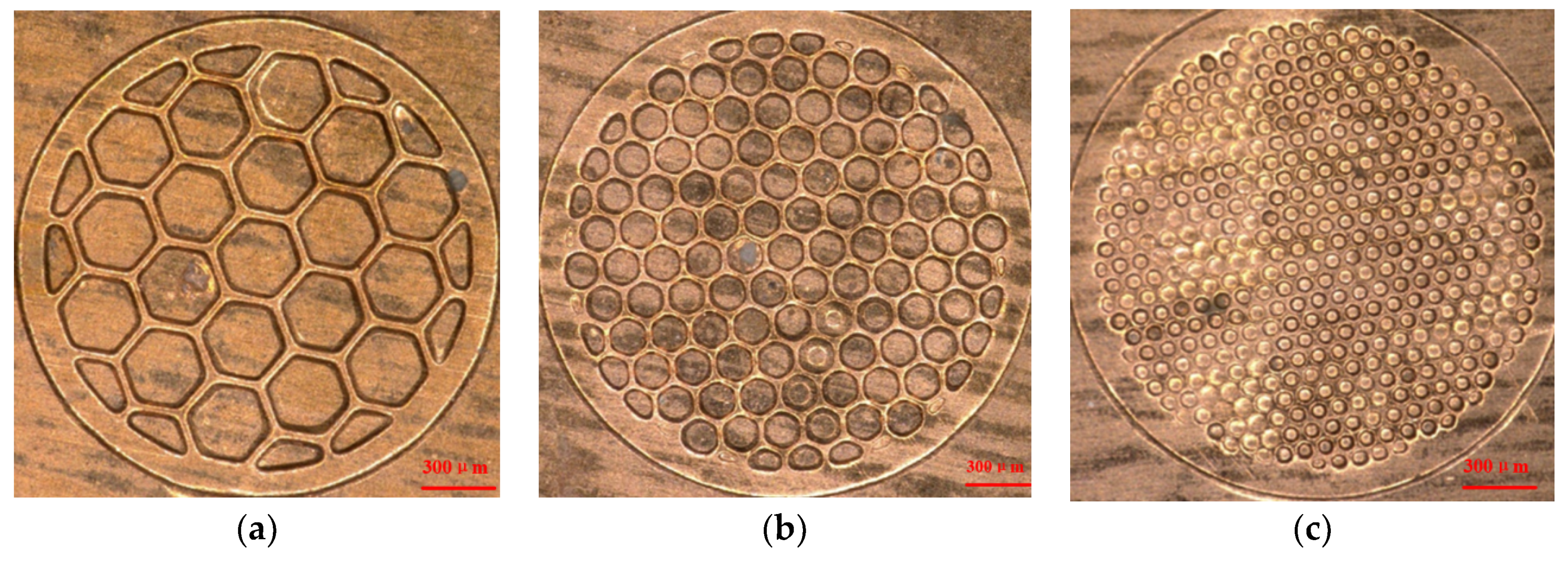
Figure 5 shows the optical images of copper foil deformation transferred from the 50# mold, 100# mold, and 230# mold. Figure 5a,c indicates that the hexagonal structures fabricated on copper foil with the 50# mold are clearer and deeper than those fabricated on copper foil with the 100# mold. The depth of hexagonal structures fabricated on copper foil with the 230# mold is shallower, and uniformity is inferior to hexagonal structures transferred from the 50# mold and 100# mold. This indicates that the smaller hexagonal holes have a higher resistance than that of large hexagonal holes.

3.2. The Analysis of Mechanical Properties and Laser Shock Forming Mechanism of Copper Foil

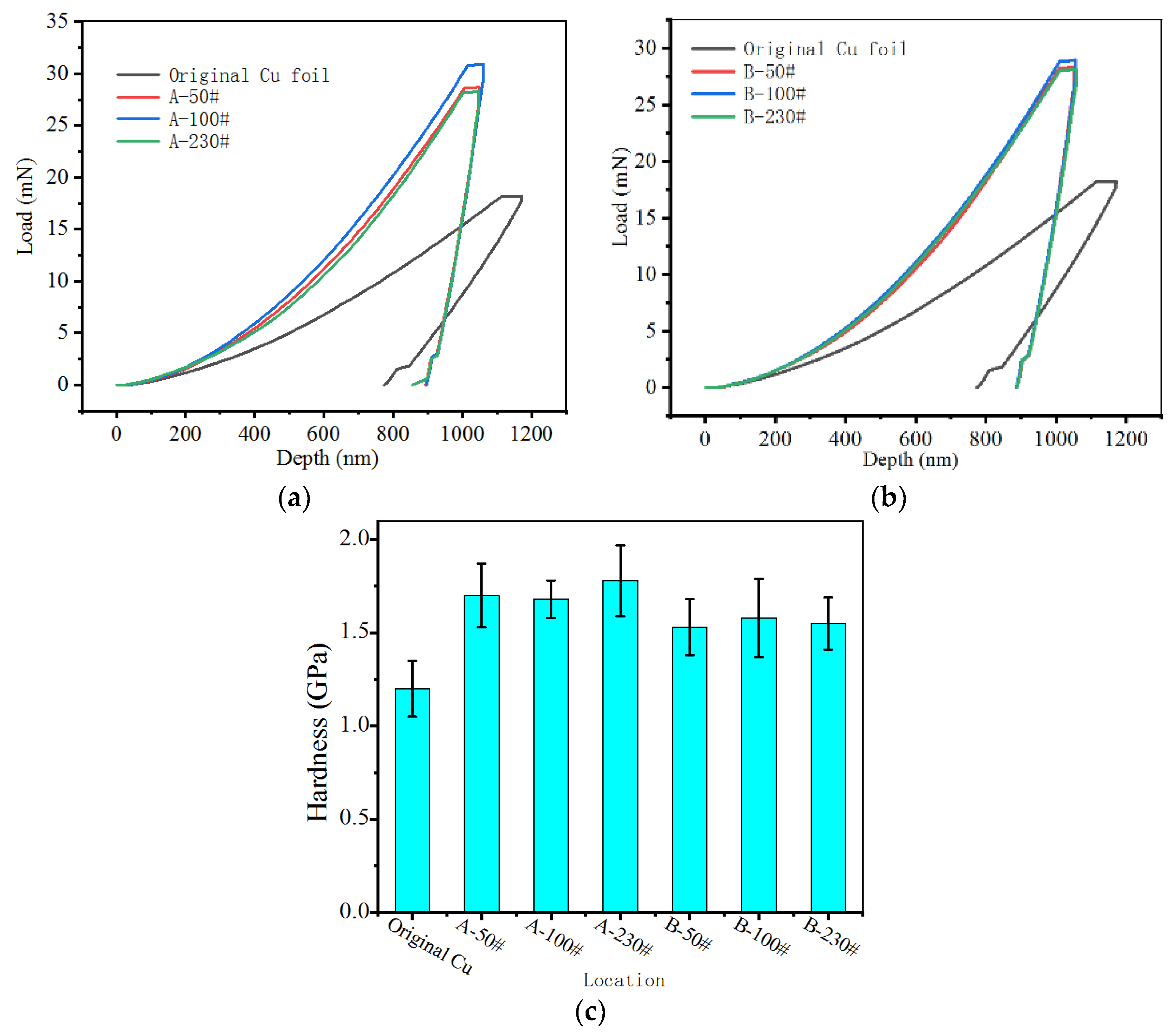
The copper foil surface formed various hexagonal structures and plastic deformation after laser shock on different molds, which changed the mechanical properties of the shocked surface. In order to investigate the hardness of the hexagonal structures on copper foil, we measured nanoindentation hardness of laser-shocked copper foil in different locations. Location A is the groove between the hexagonal structures, and location B is the center of the hexagonal structure. In the paper, the indentation depth of the nanohardness test is 1000 nm. The nanohardness of each sample was measured three times at locations A and B. The hardness error bars in Figure 6b are calculated based on the hardness data of three nanoindentation test results.
Figure 6 shows the nanoindentation load-depth curves of locations A and B on the hexagonal structure. It can be seen from Figure 6a that the load of location A of the copper foil is higher than that of the original copper foil when the depth into the surface is the same, which indicates the hardness of location A on the copper foil is improved after laser shock. Meanwhile, compared to the hardness of location A, the load of location B is lower with the same depth into the surface. The hardnesses of locations A and B on copper foil shocked with various molds are shown in Figure 6c. The hardness of the original copper foil is about 1.2 GPa, while the hardness of location A on the copper foil (transferred from 50# mold) increases to 1.7 GPa. The hardness of location B on the copper foil transferred from the 50# mold is about 1.5 GPa. The hardness of location A on the copper foil transferred from 50#, 100# and 230# is basically same. It was found that the hardness of the copper foil after laser shock was enhanced, and the hardness of location A was higher than that of location B.
The 3D morphology of the hexagonal structures on copper foil in high magnification is presented in Figure 7. It can be seen from Figure 7a that the extrusion deformation of the copper foil is concentrated in the edge area of the hexagon, and the groove bottom of the copper foil is squeezed by shock wave. The copper foil is severely extruded in the laser shock process and generates large plastic deformation. Large plastic deformation and compression in grooves were also observed in the 3D morphology of a single hexagonal structure in high magnification. In Figure 7b, the deformation and extension of shocked copper foil can also be seen obviously, but the hexagonal structure on the copper foil is slightly similar to a circle. The images of the hexagonal structures in Figure 7 indicates the process of squeezing, bending, and extending the copper foil in laser shock forming. The plastic deformation of copper foil is equivalent to being rolled in an ultrashort time, which makes the copper work harden [19,20].

3.3. The Analysis of Cross-Sectional Deformation and Microstructure Change of Copper Foil after Laser Shock

To investigate the deformation mechanism of the copper foil on mold, the cross-section images of shocked copper foil were observed by an optical microscope. The cross section of shocked copper foil was obtained by EDM and then embedded into a square epoxy block. The cross section of the epoxy block was ground with different sandpapers and polished to mirror surface. Figure 8 shows the integral and local cross-section images of copper foil deformation on 50# mold with a laser energy of 0.8 J. The cross-section image of the copper foil indicates that copper foil above the hexagon side of the 50# mold was pressed and bent, in which the copper foil was shocked in the hexagonal holes of mold. The copper foil above the hexagonal holes was pressed into the hexagonal hole, and the hexagonal structures were finally formed on copper foil surface. As shown in Figure 8b, the copper foil was bent to an angle of nearly 90°. The thickness of the copper foil was respectively thinned to 24 and 21.4 μm at a right angle. Compared with the original copper foil thickness of 30 μm, the thickness of copper foil after laser shock on mold was reduced by 6 and 8 μm, which illustrates how the copper foil generated severe plastic deformation under the effect of laser shock pressure.
Figure 9 shows the cross-section images of copper foil shock on 50# and 230# mold (polished with 1.5 W polishing paste (6000#)). In Figure 9a, the cross-section images of copper foil shock on 100# mold indicates that copper foil above the hexagon side is also squeezed by shock wave pressure. The copper foil was bent at the corner of the hexagon side, and hexagonal structures were formed on the copper foil. The copper foil generated a plastic deformation with a large displacement in the laser shock process, and the thickness of the copper foil was thinned to 27 μm at the right angle side. The cross-section images of the copper foil that was transferred from the 230# mold are presented in Figure 9b. The copper foil was bent at the hexagon side, and it generated plastic deformation and pressed into the mold hole. Because of the small size of the hexagon hole on the 230# mold (side width: 30 μm, diameter of hole: 80 μm, pitch of hexagon hole: 110 μm), the copper foil produces a small deformation on the 230# mold after laser shock, but the copper foil is also thinned at the right angle of the hexagon side (minimum thickness: 22 μm).
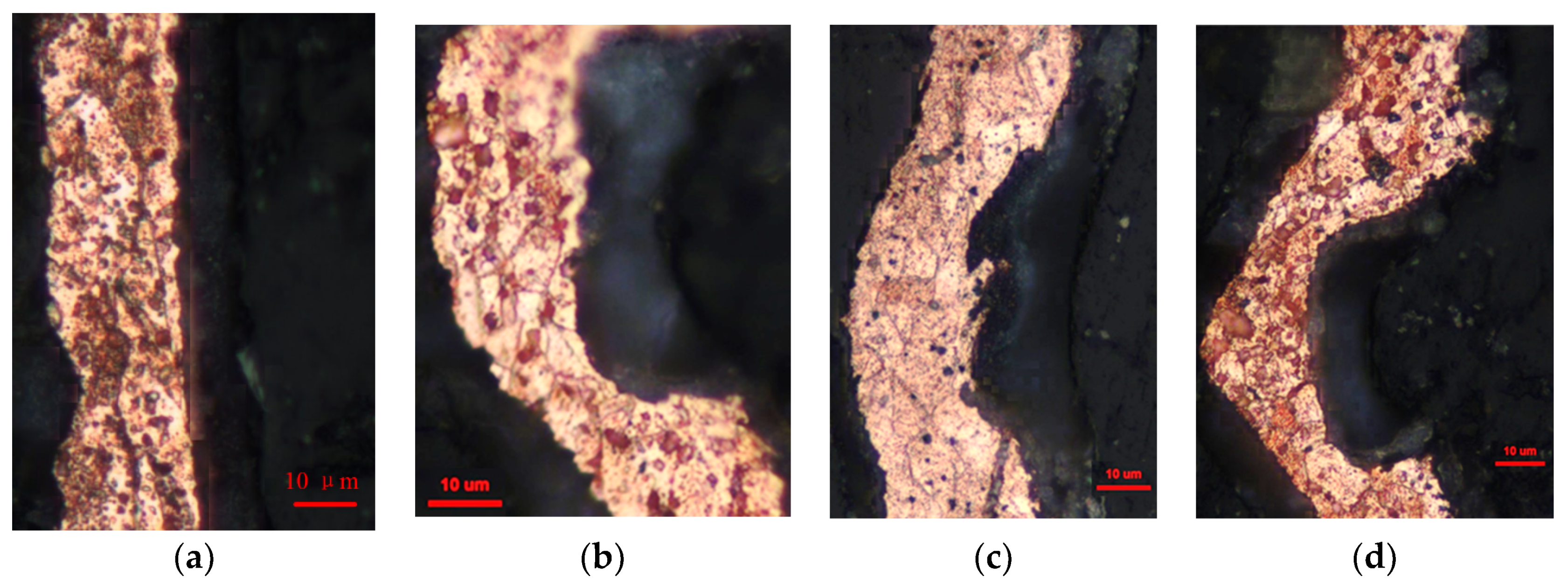
The copper foil after laser shock was embedded in epoxy resin and polished with 1.5 W polishing paste (6000#), and then the cross section of the copper foil was corroded by a FeCl3 solution. Figure 10 shows the microstructure images of the copper foil laser shocked on the 50# mold, 100# mold, and 230# mold. The microstructure image of the original copper foil’s cross section indicates that the grain size of the original copper foil seemed very general. Figure 10b shows the microstructure image of copper foil shocked on the 50# mold, in which the copper foil above the hexagon side is severely squeezed and bent by shock wave. The copper foil generated obvious plastic deformation and was thinned at the right angle of the hexagon side. Compared to the cross-sectional microstructure of the original copper foil, the cross section of the copper after laser shock in Figure 10b appears to have a clear grain boundary, and the grain of the copper foil is refined. The cross-sectional microstructure of the copper foil shocked on the 100# mold is presented in Figure 10c. The copper foil was also pressed into a hexagonal hole, and the copper on the hexagon side was stretched to both sides. The copper foil generated apparent plastic deformation after shocking on the 100# mold with a laser energy of 0.8 J. The external ultrahigh shock wave pressure broke the grain boundary equilibrium and eventually caused new grains and grain boundaries to form in the copper foil.
The grain size of the copper foil shocked on the 100# mod is smaller than that of the original copper foil. The cross-sectional microstructure image of copper foil shocked on the 230# mold is also provided in Figure 10d. The copper foil shocked on the 230# mold generates plastic deformation at the right angle of the hexagon side after laser shock. It can be found that the grain boundaries of laser shocked copper foil are clear, and the grains are also refining.
A laser-induced, high-pressure shock wave promptly pressed the copper foil on the mold. Due to the 50# mold having the largest hexagon hole, the copper foil above the hexagon hole was easily pressed into the hexagon hole under the same pressure. According to the research of both Liu and Hu et al., although the copper foil would produce plastic deformation when the copper foil was pressed into a small hole on the mold, at the same time, the copper foil was subject to a greater resistance [5,6]. Under the same laser energy, the copper foil above the 50# mold will generate larger deformation and form deeper hexagonal structures after laser shock, while the copper foil above the 100# mold and 230# mold generates a shallow hexagonal structures. The copper foil was extruded into the mold hole, and the copper on the mold side was squeezed by shock wave. The large plastic deformation was generated on the copper foil after laser shock. Both Cheng and Yang observed the changes of dislocation and microstructure in laser shock imprinted metallic foil by TEM [1,4]. Therefore, under the effect of external shock wave pressure, the copper foil produces severe plastic deformation and forms new grain, which is the equivalent to rolling copper in sections. In Figure 10, compared to the original copper foil’s cross section, refined grains were observed in the microstructures of a copper foil cross section, which proves that grain refinement occurs in the laser shock forming process. With the increasing of pulse laser energy, the laser will induce a shock wave with higher peak pressure, and copper foil would generate large deformations and fabricate deeper hexagonal structures.

4. Conclusions

In this work, regular hexagonal structures were fabricated on copper foil with different molds by laser shock. The pulse laser energy, mechanical properties, forming mechanism, and cross-sectional microstructures were investigated in this paper. The following conclusions can be drawn:
(1)
Three sizes of hexagonal structures were successfully manufactured on copper foil by the laser shock process. The depth of hexagonal structures increased with the increasing of pulse laser energy, and the copper foil on the 50# mold formed deeper hexagonal structures under the same pulse laser energy.
(2)
The mechanical properties of the copper foil on the hexagon side of the mold were improved after laser shock. The copper foil generated severe plastic deformations and was bent at the right angle of the hexagon side, in which the copper foil became thin.
(3)
The cross-sectional microstructure of the copper foil changed after laser shock. The grains of the copper foil were refined by shock wave pressure.

Author Contributions

Conceptualization, D.H. and J.M.; methodology, D.H. and J.M.; software, J.M.; validation, D.H. and J.M.; formal analysis, J.M.; investigation, D.H. and J.M.; resources, D.H.; data curation, D.H. and J.M.; writing—original draft preparation, D.H. and J.M.; writing—review and editing, D.H. and J.M.; visualization, D.H.; supervision, D.H. and J.M.; project administration, D.H.; funding acquisition, D.H. All authors have read and agreed to the published version of the manuscript.

Funding

This research was funded by the Natural Science Foundation of Jiangsu Province (No. BK20190635), the Jiangsu Planned Projects for Postdoctoral Research Funds (No. 2019K228) and a project funded by the Priority Academic Program Development of Jiangsu Higher Education Institutions (PAPD).

Conflicts of Interest

The authors declare no conflict of interest.

References

  1. Gao, H.; Hu, Y.; Xuan, Y.; Li, J.; Yang, Y.; Martinez, R.V.; Li, C.; Luo, J.; Qi, M.; Cheng, G.J. Large-scale nanoshaping of ultrasmooth 3D crystalline metallic structures. Science 2014, 346, 1352–1356. [Google Scholar] [CrossRef] [PubMed]
  2. Tahan, G.; Arrigoni, M.; Bidaud, P.; Videau, L.; Thevenet, D. Evolution of failure pattern by laser induced shockwave within an adhesive bond. Opt. Laser Technol. 2020, 129, 106224. [Google Scholar] [CrossRef]
  3. Ngiejunbwen, L.A.; Shangguan, J.; Asamoah, E.; Ren, Y.; Ye, Y.; Tong, Y. Experimental investigation of sheet metal forming of Aluminum 2024 using nanosecond pulsed Nd: YAG laser. Opt. Laser Technol. 2021, 133, 106528. [Google Scholar] [CrossRef]
  4. Man, J.; Zhao, J.; Yang, H.; Song, L.; Liu, D. Study on laser shock imprinting nanoscale line textures on metallic foil and its application in nanotribology. Mater. Des. 2020, 193, 108822. [Google Scholar] [CrossRef]
  5. Hu, Y.; Kumar, P.; Xu, R.; Zhao, K.; Cheng, G.J. Ultrafast direct fabrication of flexible substrate-supported designer plasmonic nanoarrays. Nanoscale 2016, 8, 172–182. [Google Scholar] [CrossRef] [PubMed]
  6. Liu, H.; Sun, X.; Shen, Z.; Li, C.; Sha, C.; Li, L.; Gao, S.; Ma, Y.; Wang, X. The size effect on deformation behavior in microscale laser shock flexible drawing. Opt. Laser Technol. 2016, 86, 93–102. [Google Scholar] [CrossRef]
  7. Zheng, C.; Sun, S.; Zhang, G.; Song, L.; Ji, Z. Effect of confining overlay in micro scale laser bulge forming. Appl. Surf. Sci. 2013, 285, 477–482. [Google Scholar] [CrossRef]
  8. Wang, X.; Qiu, T.; Shen, Z.; Zhang, D.; Ma, Y.; Gu, Y.; Liu, H. Forming properties of a microscale laser dynamic flexible forming technique. Mater. Manuf. Process. 2016, 31, 745–750. [Google Scholar] [CrossRef]
  9. Ehrhardt, M.; Lorenz, P.; Lotnyk, A.; Romanus, H.; Thelander, E.; Zimmer, K. Pattern transfer of sub-micrometre-scaled structures into solid copper by laser embossing. Phys. Procedia 2014, 56, 944–950. [Google Scholar] [CrossRef] [Green Version]
  10. Ye, C.; Cheng, G.J. Scalable patterning on shape memory alloy by laser shock assisted direct imprinting. Appl. Surf. Sci. 2012, 258, 10042–10046. [Google Scholar] [CrossRef]
  11. Yang, H.; Xiong, F.; Liu, K.; Man, J.; Chen, H.; Liu, H.; Hao, J. Research on temperature-assisted laser shock imprinting and forming stability. Opt. Lasers Eng. 2019, 114, 95–103. [Google Scholar]
  12. Shen, N.; Ding, H.; Bowers, R.; Yu, Y.; Pence, C.N.; Ozbolat, I.T.; Stanford, C.M. Surface micropatterning of pure titanium for biomedical applications via high energy pulse laser peening. J. Micro Nano-Manuf. 2015, 3, 011005. [Google Scholar] [CrossRef]
  13. Wang, X.; Li, L.; Shen, Z.; Sha, C.; Gao, S.; Li, C.; Sun, X.; Ma, Y.; Liu, H. Experimental investigation on: Laser shock micro-forming process using the mask and flexible pad. Opt. Lasers Eng. 2017, 88, 102–110. [Google Scholar] [CrossRef]
  14. Wang, X.; Shen, Z.; Gu, C.; Zhang, D.; Gu, Y.; Liu, H. Laser indirect shock micro-embossing of commercially pure copper and titanium sheet. Opt. Lasers Eng. 2014, 56, 74–82. [Google Scholar] [CrossRef]
  15. Li, J.; Zhang, R.J.; Jiang, H.; Cheng, G.J. Scalable nano-patterning of graphenes using laser shock. Nanotechnology 2011, 22, 475303. [Google Scholar] [CrossRef] [PubMed]
  16. Man, J.; Yang, H.; Wang, Y.; Chen, H.; Xiong, F. Study on controllable surface morphology of the micro-pattern fabricated on metallic foil by laser shock imprinting. Opt. Laser Technol. 2019, 119, 105669. [Google Scholar] [CrossRef]
  17. Nagarajan, B.; Castagne, S.; Wang, Z.K. Investigation of copper foil thinning behavior by flexible-pad laser shock forming. Key Eng. Mater. 2013, 535–536, 306–309. [Google Scholar] [CrossRef]
  18. Fabbro, R.; Fournier, J.; Ballard, P.; Devaux, D.; Virmont, J. Physical study of laser-produced plasma in confined geometry. J. Appl. Phys. 1990, 68, 775–784. [Google Scholar] [CrossRef]
  19. Lu, Q.; Shinsuke, I.; Wang, F.; Zhang, C.; Lu, Y.; Nastasi, M.; Cui, B. Influence of laser shock peening on irradiation defects in austenitic stainless steels. J. Nucl. Mater. 2017, 489, 203–210. [Google Scholar] [CrossRef] [Green Version]
  20. Pan, X.; Wang, X.; Tian, Z.; He, W.; Shi, X.; Chen, P.; Zhou, L. Effect of dynamic recrystallization on texture orientation and grain refinement of Ti6Al4V titanium alloy subjected to laser shock peening. J. Alloy. Compd. 2021, 850, 156672. [Google Scholar] [CrossRef]
Figure 1. (a) The schematic of microstructures fabricating on copper foil by laser shock deformation; (b) the image of 50# mold.
Coatings 10 01264 g001
Figure 2. The morphology of copper foil shocked with different laser energies and molds: (a) a pulse laser energy of 0.45 J, 50# mold, (b) a pulse laser energy of 0.45 J, 100# mold, (c) a pulse laser energy of 0.8 J, 50# mold, (d) a pulse laser energy of 0.8 J, 100# mold.
Coatings 10 01264 g002
Figure 3. (a) The morphology of copper foil shocked with pulse laser energy of 0.45 J and 230# mold; (b) the morphology of copper foil shocked with laser energy of 0.8 J and 230# mold.
Coatings 10 01264 g003
Figure 4. The profile curves of hexagonal structures fabricated with different laser energies: (a) transferred from 50# mold; (b) transferred from 100# mold; (c) transferred from 230# mold.
Coatings 10 01264 g004aCoatings 10 01264 g004b
Figure 5. (a) The images of copper foil shocked on various molds: (a) 50# mold; (b) 100# mold; (c) 230# mold.
Coatings 10 01264 g005
Figure 6. (a) The load-depth curves of the location A of hexagon structure; (b) the load-depth curves of location A of the hexagon structure; (c) the hardness of locations A and B of the hexagon structure.
Coatings 10 01264 g006
Figure 7. (a) The 3D morphology of a hexagonal structure (50# mold, 0.6 J) in high magnification; (b) the 3D morphology of hexagonal structures (100# mold, 0.6 J) in high magnification.
Coatings 10 01264 g007
Figure 8. (a) The cross-section images of copper foil shocked on 50# mold with a laser energy of 0.8 J; (b) the local enlarged image of the copper foil’s cross section after laser shock.
Coatings 10 01264 g008
Figure 9. (a) The cross-section images of copper foil shocked on 100# mold with a laser energy of 0.8 J; (b) the cross-section images of copper foil shock on 230# mold with a laser energy of 0.8 J.
Coatings 10 01264 g009
Figure 10. The cross-sectional microstructure images of the copper foil after laser shock: (a) the original copper foil; (b) the copper foil shocked on 50# mold with a pulse laser energy of 0.8 J; (c) the copper foil shocked on 100# mold with a pulse laser energy of 0.8 J; (d) the copper foil shocked on the 230# mold with a pulse laser energy of 0.8 J.
Coatings 10 01264 g010
Publisher’s Note: MDPI stays neutral with regard to jurisdictional claims in published maps and institutional affiliations.