1. Introduction
The recent popularity of Bi
2O
3 as a p-type semiconductor as a research topic, is mainly due to its attractive physical properties, which include wide optical bandgap energies that range from about 2.0 to 3.9 eV, high dielectric permittivity, good photocatalytic activity, high refractive index, oxide ion conductivity and good photoluminescence (PL) [
1,
2]. Bi
2O
3 also has the potential to be used in a number of modern applications, including their applications as supercapacitors, optical coatings, optoelectronic devices, gas sensors, microwave integrated circuits, solar cells, etc. [
3,
4].
It is common knowledge that Bi
2O
3 has five different polymorphic forms that are denoted as α-Bi
2O
3 (monoclinic), β-Bi
2O
3 (tetragonal), γ-Bi
2O
3 (body centred cubic), δ-Bi
2O
3 (face centred cubic) and ε-Bi
2O
3 (orthorhombic) [
3,
4]. The α-Bi
2O
3 phase is the favourite research candidate amongst the different polymorphic forms, due to its high refractive index, good photocatalytic activity and stability at room temperature, while the α-Bi
2O
3 nanostructure is well-known as a visible light active semiconductor. This makes it a very suitable candidate for solid-state white lightening optoelectronics, optical switches, ultra-short pulse generators and nonlinear optical fibre devices [
1,
5,
6,
7]. The β-Bi
2O
3 on the other hand, has shown tremendous potential in photo-electrochemical and photocatalytic applications [
8].
Research literature indicates that the Bi
2O
3 films have been prepared by various methods, such as the vapor transport method [
7], spray pyrolysis technique, pulsed laser deposition (PLD), chemical vapor deposition (CVD), sputtering, electro-deposition and sol–gel technique [
6]. Reported results indicate that it is possible to grow good quality oxide films at comparatively low substrate temperatures with PLD without the need for annealing treatment. These films exhibit highly textured morphologies with improved orientation which increases the probability of growing better quality thin films with improved luminescence and optical properties. In addition, PLD also has the potential to deposit various thicknesses of the films, which opens up the opportunity for the simultaneous use of several distinct materials as targets and the opportunity for the in situ deposition of hetero-structures with atomic precision or with complex oxides. [
9,
10]. Recent articles on the use of PLD for Bi
2O
3 thin film deposition reported cost-efficient BK7 glass slide deposition with substrate temperatures ranging between 300 and 600 °C and included a report on the crystal structure, morphology and optical properties of the deposited material. Results which indicated the formation of various energy bandgap values for the different films may have useful applications in several optoelectronics industries [
11].
PL is also a very useful technique to investigate the structure, the electronic band transitions and the intrinsic and extrinsic defects of these deposited materials [
12], and has extensively been used to study the optical variations of α-Bi
2O
3 which can potentially be used in numerous applications [
12,
13,
14]. Li et al. [
15] reported the layer-by-layer assembly preparation of thin-film Bi
2O
3. The excitation spectra of these Bi
2O
3 films indicated a very characteristic and intense peak at 390 nm, which was very close to the 388 nm band (3.2 eV), which is normally attributed to the band gap of excited Bi
2O
3. The strong green emission of Bi
2O
3 is ascribed to intraionic transitions in Bi
3+ (
3P
1-
1S
0 transitions) [
16,
17,
18]. The weak emission intensity of Bi ions in Bi
2O
3 restricts its application as a light emitting phosphor [
13,
19,
20]. Research, however, proved that the doping of Bi
2O
3 with rare earths (REs) enhances the PL properties of Bi
2O
3 nanocrystals in the visible to infrared region [
1,
2]. It is well known that the excitation of RE ions in the UV-visible region results in the emittance of sharp emissions bands in the ultraviolet to the far infrared region due to their 4f–4f or 5d–4f transitions [
1,
2,
20]. Research confirmed that the inclusion of RE ions into the Bi
2O
3 crystal lattice improved the luminescence properties of the Bi nanocrystals [
2]. Among the RE ions, holmium (Ho
3+) is one of the desirable candidates to be used as an activator because of its favourable energy level structure and multiple meta-stable energy levels [
21]. Ho
3+ ions are used for laser action at different wavelengths, from 550 nm to 3.9 µm, in a variety of hosts [
22]. Results obtained by Premkumar et al. [
23] indicated that the inclusion of Ho
3+ into a YAlO
3 nanophosphor produced multiple meta-stable Ho
3+ energy levels due to the complexity of its 4f
10 energy level system, which produced multiple emissions at various wavelengths ranging from the visible to the infrared region [
1,
23]. The green emission, which dominates the blue and red emissions, is attributed to the
5F
4/
5S
2 →
5I
8 transitions present in the Ho
3+. This intense green luminescence can be used in the lamp industry, in cathode ray tube (CRT) manufacturing, as field emission displays (FEDs), in security printing and even in biologically-oriented applications [
24,
25,
26,
27]. Additionally, the NIR emissions may have applications in remote sensing, military applications and weather forecasting, or for atmospheric pollution detection [
28,
29]. In addition, the ionic radius of the Ho
3+ ion (0.90 Å) is nearly equal to that of the Bi
3+ ion (1.03 Å) in Bi
2O
3 [
30]; therefore, the Ho
3+ ions are easily substituted into Bi
3+ in the Bi
2O
3 crystal lattice without any charge compensation. In our pervious study we reported on the structural, optical, photoluminescence and photocatalytic properties of the monoclinic Bi
2O
3:Ho
3+ nanopowder that was synthesized by the co-precipitation method, which showed a strong green emission with greater photocatalytic activity for degradation of organic dye under UV–Vis light [
1]. There are only a few reports on optical and luminescence studies of RE-ion-doped Bi
2O
3 thin films [
10,
31]. Due to the strong green emission of the obtained powder [
1], it was necessary to also try to obtain efficient thin films for the different applications, especially flat panel displays (FPDs). Thin film phosphor materials have some advantages over powders in the FED environment, such as the reduction of light scattering and the good thermal contact between the screen and the faceplate [
32,
33]. The laser deposition technique has advantages over other deposition methods, because it is a purely physical mechanism without the incorporation of carbon and the stoichiometry of the target material is maintained in the deposited films [
34]. The thickness and the surface morphology can be controlled by varying, among the growth parameters, the number of laser pulses and the ambient gas pressure in the deposition chamber [
35].
This study investigated the PLD deposition of Bi2O3:Ho3+ thin films on silicon (100) substrates. The effects of deposition substrate temperatures and oxygen partial pressures on the as-prepared films’ structural, morphological, compositional, optical and luminescence properties were systematically investigated. The surface chemical states were studied by X-ray photoelectron spectroscopy (XPS), while the resulting crystal features, morphology, surface contaminations and oxygen vacancies were correlated with the PL results. The first step was to understand the material characteristics and to determine the correlations between the deposition parameters and photoluminescence properties of the Bi2O3:Ho3+ thin films. No work has not yet been reported on the luminescence studies of Ho3+-doped Bi2O3 thin films. Optimization of the deposition parameters is very important in the study of luminescent thin films. Therefore, we examined the conditions under which strong PL from Bi2O3:Ho3+ was observed.
3. Results
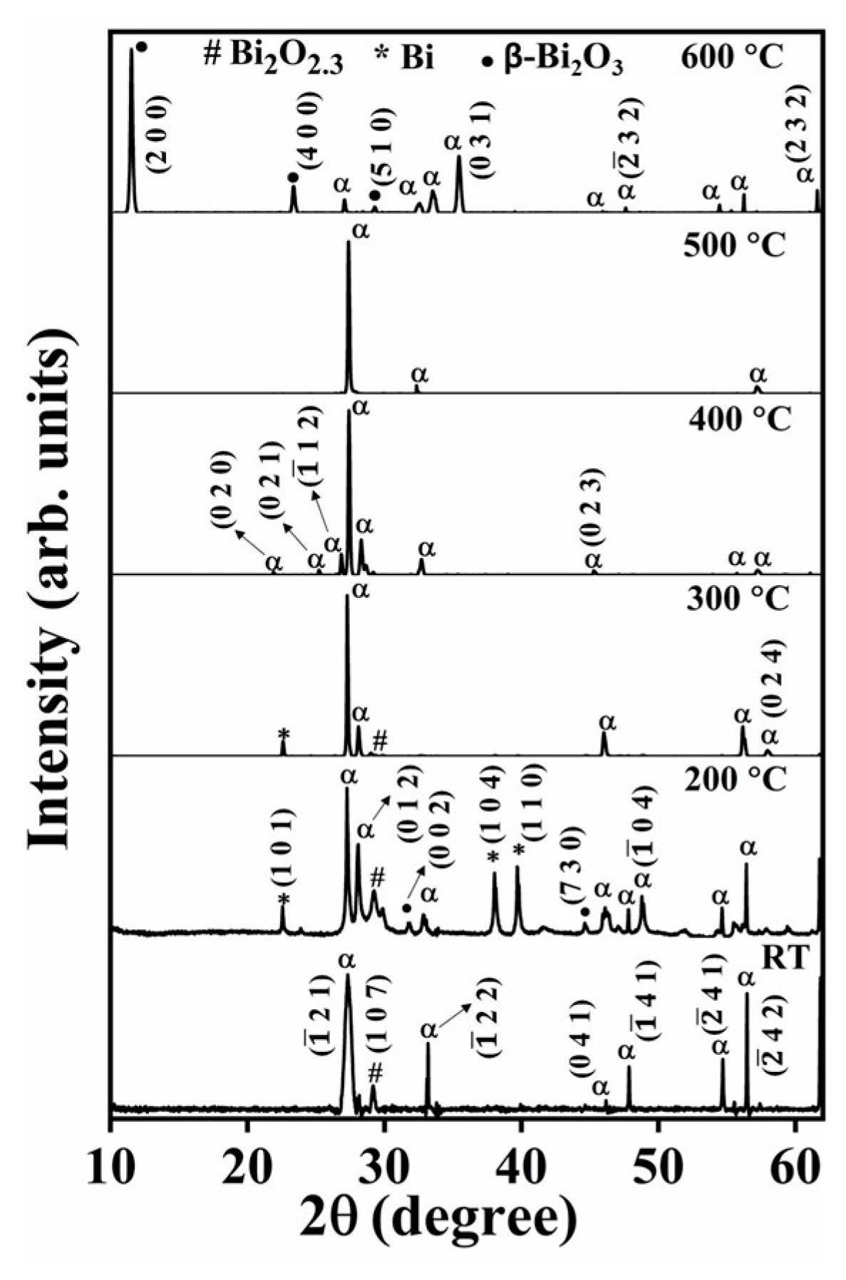
The XRD patterns in
Figure 1 show the as-deposited Bi
2O
3:Ho
3+ films on the substrates at different temperatures (T
S) which ranged between RT and 600 °C. The maximum diffraction peaks of the RT film indicated the presence of monoclinic α-Bi
2O
3 (JCPDS card 71-2274), with the main one situated at
° (
21) and a non-stoichiometric of Bi
2O
2.3 phase peak at 29.2° (JCPDS card number 76-2477). However, the XRD pattern of the film obtained for the T
S at 200 °C consisted of a mixture of Bi metal diffraction peaks at 2θ = 22.6°, 38.03° and 39.71° (JCPDS card number 85-0051), and
-Bi
2O
3 peaks at 2θ = 31.6° and 44.5° (JCPDS card number 74-1331) indicating the presence of the non-stoichiometric Bi
2O
2.3 phase and the predominant presence of the α-Bi
2O
3 phase. The XRD pattern of the T
S at 300 °C showed the presence of α-Bi
2O
3 phase accompanied by peaks attributed to Bi metal and non-stoichiometric phases. At this temperature, the
-phase peaks and some Bi metal peaks at 2θ = 38.03
° and 39.71
° disappeared, and a new α-Bi
2O
3 peak appeared at 57.9°
. At 400 and 500 °C only a single α-Bi
2O
3 phase product was observed, suggesting the complete oxidation of the bismuth thin films [
36,
37]. A further increase of T
S to 600 °C again led to the formation of mixed α-,
-Bi
2O
3 phases with the
-Bi
2O
3 peaks positioned at 2θ = 11.5°, 23.0° and 29.3° (JCPDS card number 74-2351). The results also indicate that the
-Bi
2O
3 peak positioned at 11.5° which corresponds to the (200) index plane becomes more prominent at 600 °C. The growth of the tetragonal Bi
2O
3 phase at 600 °C was also confirmed by the FESEM image (Figure 4). No additional peaks related to the presence of Ho or any other impurities were detected, and these results indicated that α-Bi
2O
3 is thermodynamically stable between 400 and 500 °C [
38].
The XRD results indicated that the synthesis of
-Bi
2O
3 and mixed α,
phases can be achieved by controlling the substrate temperature in vacuo. It is concluded that the high T
S is not suitable for obtaining pure α-Bi
2O
3 thin films. Similar results were reported by Ahila et al. [
39], who prepared Bi
2O
3 films via a constant potential anodization method, a process by which they thermally evaporated “Bi” layers onto a stainless steel substrate. These thin films were annealed at temperatures between 300 and 600 °C. The resulting layers obtained at 300, 400 and 500 °C showed diffraction peaks that correlated well with those of monoclinic α-Bi
2O
3. The results obtained for the films annealed at 600 °C, however, indicated the transformation of the α-Bi
2O
3 into the
-Bi
2O
3 phase [
39].
The diffraction peak intensity increase in
Figure 1, with the increase of the T
S, is accompanied by a decrease in the peak broadening (better defined), suggesting improvement of the crystallinity of the film at higher temperatures. The crystallite sizes “D” for the Bi
2O
3:Ho
3+ films were calculated using the Scherrer formula [
13]. The most prominent peak at 27.3° (
2 1) was used for calculating the crystallite sizes for the different temperatures (RT-500 °C) and peak at 11.5° (200) was used for 600 °C calculation. The results indicated that the crystallite size increased from RT to 400 °C and values of 47, 48, 49 and 49.5 nm were obtained at RT, 200, 300 and 400 °C respectively. This enhancement of the lattice plane orientation with an increase in temperature is attributed to an increase in the surface diffusion of the adsorbed species, resulting in an improvement in the crystal growth [
40,
41]. Similar results were also observed for ZnO [
42], ZnO:Al [
43] and ZnO:Ga [
44]. Further increases in T
S to 500 and 600 °C led to decreases of the crystallite size to 49 and 48.8 nm respectively. A possible reason may be due the poor plane orientation as a result of monoclinic Bi
2O
3 decomposition or possibly due to phase transformation from monoclinic Bi
2O
3 to tetragonal Bi
2O
3 [
45].
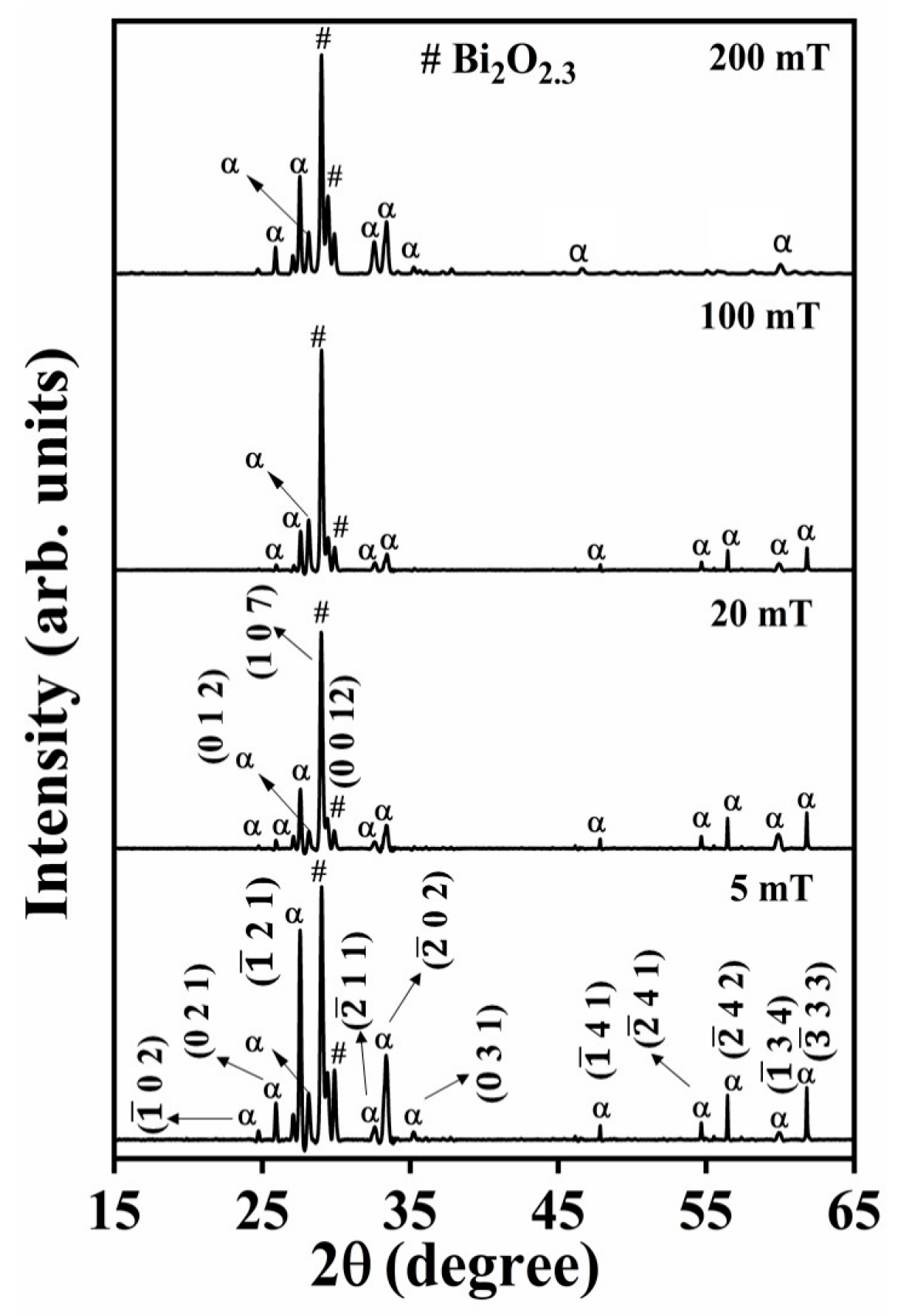
The XRD patterns of the Bi
2O
3:Ho
3+ films deposited on the Si substrates at 400 °C and in the presence of different oxygen partial pressures (5–200 mT), are reported in
Figure 2. All the diffraction peaks of the films (5–100 mT) indicate mixed α-Bi
2O
3 and non-stoichiometric phases of Bi
2O
2.3 with different peak intensities. Most of the observed peaks match those of the α-Bi
2O
3 phase, (JCPDS card number 71-2274), while the diffraction peaks of the non-stoichiometric phase of Bi
2O
2.3 (JCPDS card number 76-2477) were situated at 2θ = 29.2 (most intense) and 30.5°. There was also no evidence of the presence of Bi in metallic phase in these then oxide films. The crystallite sizes of the films also increased stepwise from 40 to 41, 43, and finally 45 nm as a function of the increases in oxygen pressures from 5 to 20, 100 and finally 200 mT and is attributed to a decrease in intrinsic crystal defects with an increase in the oxygen pressure, resulting in the improved crystallinity [
46]. Similar results were reported by Jian et al. [
47], who also observed improved ZnO thin film crystallinity at higher oxygen partial pressures.
The lattice strain (ε) was calculated using Equation (1) [
48]:
where,
is the full width at half maximum (FWHM) in radians and θ is the Braggs angle. The value of dislocation density (
) is calculated using the Equation (2) [
49]:
The results in
Table 1 indicate that the increase in crystallite size is associated with decreases in the strain and dislocation density, resulting in the improvement in the crystallinity of the Bi
2O
3:Ho
3+ thin films. The decrease in strain indicates a decrease in crystal defect concentration and the subsequent formation of high quality films. The products isolated at 500 °C and above indicated a decrease in crystallite size with an increase in strain and dislocation density which could be due to the phase transformation [
48].
The stresses of the prepared films were calculated using the Equation (3) [
48]:
where E is the Young’s modulus of the Bi
2O
3 thin film (28 GPa) [
6,
49] and ε is the lattice strain. The estimated values of the stress in the films which were grown at the different substrate temperatures are tabulated in
Table 1, with a positive sign indicating that the films are in a state of tensile stress. The results clearly indicate that an increase in substrate temperature increased the atomic mobility, and subsequently reduced structural defects and thus caused a decrease in the crystal stress [
48]. An increase in stress was observed for the films obtained at 500 °C and above, possibly due to a change in the morphology of the film [
50].
The reflection intensities for each XRD pattern contain extra information related to the preferential or random growth of the polycrystalline thin films. Quantitative information concerning the preferential orientation and texture coefficient (TC
hkl) was calculated with Equation (4) [
48] and the results are reported in
Table 1.
where I
(hkl) is the measured relative intensity of a plane (hkl) and I
o(hkl) the standard intensity of the plane (hkl) as taken from JCPDS data, and n is the total number of reflections. The gradual change of the film texture in a (
) plane was used to evaluate the texture coefficient of each isolated film. The results in
Table 1 indicate an increase in texture coefficient which is associated with the substrate temperature increase and reaches a maximum at 400 °C, and then decreases moderately with a further increase to 500 °C, but decreases substantially when the temperature is increased to 600 °C. The calculated texture coefficient for the film deposited at 400 and 500 °C exceeded one (unity) and is an indication that the film was preferentially oriented along the (
) plane [
6,
51].
The crystal size, strain, stress and dislocation of the deposited films as functions of O
2 partial pressure, are reported in
Table 2. The results indicate that the crystallite size increase which is observed is associated with a decrease in the strain, in the stress and in the dislocation density with an increase in the O
2 partial pressures. This is indicative of improved crystallinity in the newly formed Bi
2O
3:Ho
3+ thin films and a decrease in crystal defect concentrations. TC
hkl values <1 were obtained for all the different O
2 partial pressures, which implies a lack of grained growth in the hkl direction ((
) plane) considered [
6].
In
Figure 1 and
Figure 2, the relative XRD peak intensities of certain crystal planes are noticeably different, indicating a variation among the growth rates of certain crystal planes [
52]. The different deposition conditions (different substrate temperature and pressure) lead into the anisotropic growth of crystals, random orientation of crystal planes and different shapes and thicknesses of the thin films. Similar results were observed on the XRD patterns of indium tin oxide thin films that were grown by direct current magnetron sputtering at different O
2 partial pressures [
53]. Dev et al. [
6] reported on the structural and optical properties of undoped and B doped Bi
2O
3 thin films. They observed variations in the intensities of the (11
) and (02
) diffraction peaks in the α-Bi
2O
3 due to the enhancement of stacking defects in the Bi
2O
3 lattice structure, the segregation of the B dopant around the grain boundaries and the change of intrinsic strain through doping. Kumari et al. [
18] studied Bi thin films that were deposited by thermal evaporation at varying substrate temperatures and they found that the substrate temperature strongly affected the surface morphology and crystalline orientation of the Bi thin films.
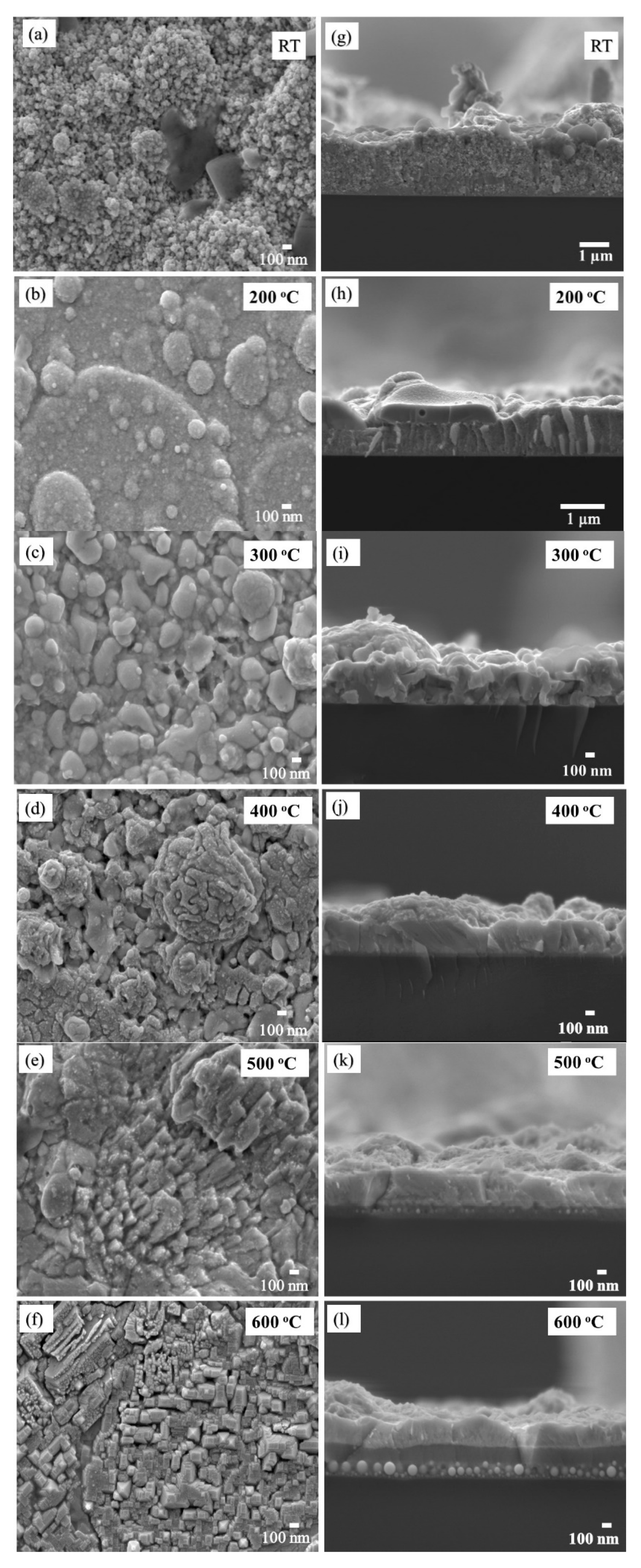
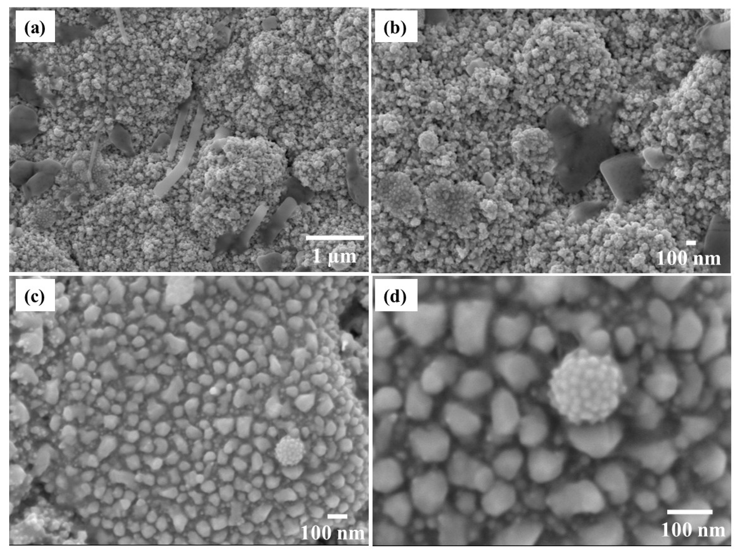
The FESEM images of the Bi
2O
3:Ho
3+ films deposited at different temperatures (T
S = RT, 200, 300, 400, 500 and 600 °C,) are reported in
Figure 3a–f respectively. The images clearly indicate a change in surface morphology which is associated with an increase in substrate temperature and that the morphologeis of the thin films were strongly dependent on the deposition conditions. The images reveal non-uniform morphology without any cracks. At lower substrate temperatures (
Figure 3a for RT), the films had small grains sizes and poor crystallinity. At higher temperatures (200, 300 and 400 °C), the surfaces appeared rough, and agglomerated particles were distributed inhomogeneously on the substrate surface
Figure 3b–d. The aggregation of small crystalline grains was also evident under these conditions. At a substrate temperature of 500 °C (
Figure 3e) the film consisted of small crystallites which were well distributed over the entire substrate area and clearly revealed a clear “step-and-terrace structure” [
54,
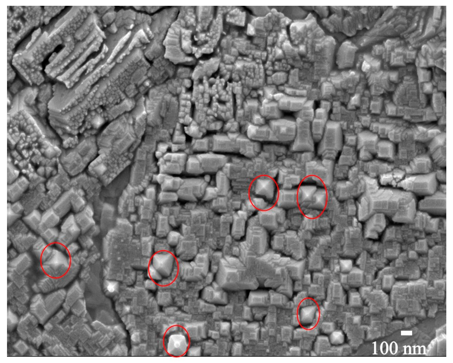
55]. At 600 °C, the film showed the same “step-and-terrace structure” along with a few tetragonal bipyramidal crystals which are highlighted with red circles in
Figure 4. The appearance of the tetragonal crystals at 600 °C is attributed to the dominance of the
-Bi
2O
3 phase, which is also confirmed by the XRD results. The Bi and O atoms contain a lot of kinetic energy when they arrive at the Si substrate surface during the deposition process. At lower substrate temperatures (RT), the atoms have low mobility and the total energy (≡ kinetic energy plus thermal energy) rather supports a diffusive force which is unable to overcome the interaction or attractive force between the atoms and the substrate surface. This results in a decrease in grouping which is needed for nucleation and island formation, which ultimately leads to the growth of small grains on the substrate [
56,
57]. An increase in substrate temperature increases the total thermal energy of the atoms, which increases the surface diffusion of the Bi and O atoms. These atoms also do not have sufficient time to nucleate since they arrive on the surface of the substrate with high kinetic energy [
58]. The collisions among the diffusing atoms are therefore greater than those between the atoms and the substrate surfaces, and tend to adhere to one another, resulting in the nucleation of tiny nanoclusters at the higher substrate temperatures [
56,
58]. At 500 and 600 °C, the kinetic energy of the atoms is even higher, resulting in an increase in atom mobility and enhanced surface diffusion which ultimately results in differences in surface morphology [
59]. Four different magnification FESEM images of the sample deposited at RT are shown in
Figure 5. The irregular shape and non-uniformity of the film can clearly be observed.
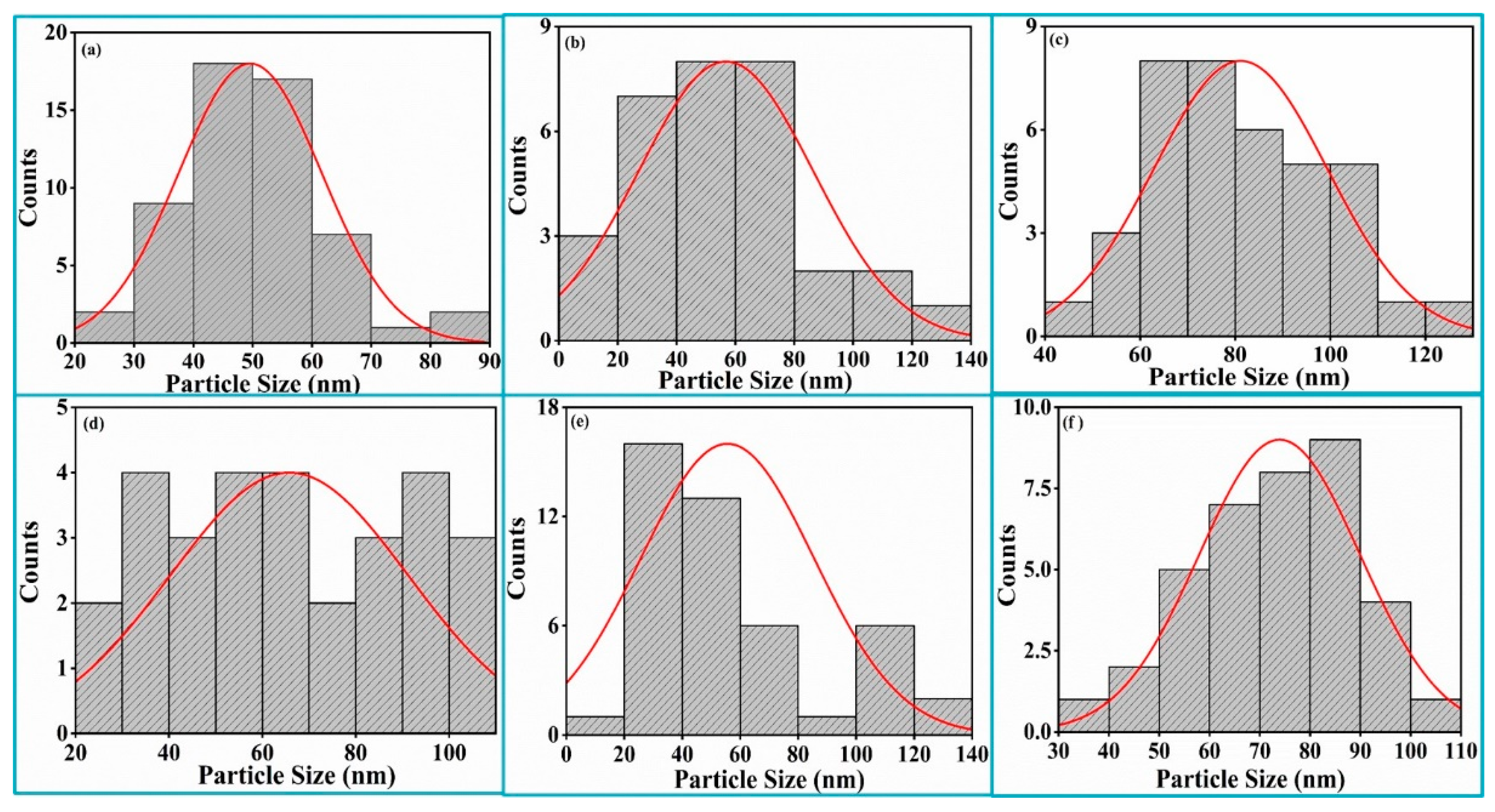
Average particle size was calculated by choosing isolated particles from the FESEM using ImageJ software (version 1.53e). Histograms of the particle size distribution pattern were fitted with Gaussian distributions to calculate average particle sizes of the Bi
2O
3:Ho
3+ thin films deposited at different substrate temperatures. The average particle size was 50 nm for RT, 57 nm for 200 °C, 81 nm for 300 °C, 66 nm for 400 °C, 56 nm for 500 °C and 74 nm for 600 °C, as shown in
Figure 6a–f. The average particle size increased until the substrate temperature of 300 °C due to the effects on nucleation, crystal growth and the aggregation of small grains. The decrease in the average particle size with a further increase in the substrate temperature up to 500 °C was due to less agglomeration of the small grains. The average particle size again increased at a higher substrate temperature (T
S = 600 °C), possibly due to the partial phase transformation to the β-Bi
2O
3, resulting in nucleation along the (200) plane of β-Bi
2O
3. The cross-section images of the Bi
2O
3:Ho
3+ films at different substrate temperatures are given in
Figure 3g–l and the average thickness of each thin film was calculated using ImageJ software. These calculations indicate a decrease in thickness as a function of temperature increase, and thickness was calculated as 1380 ± 13, 855 ± 15, 319 ± 16, 307 ± 13, 303 ± 12 and 218 ± 10 nm for the substrate temperatures of RT, 200, 300, 400, 500 and 600 °C, respectively. This may have been due to densification, crystallization and the formation of large grain sizes, as previously reported by Tay et al. [
60]. Additionally, at the high substrate temperatures (500 and 600 °C), interdiffusion of the Bi, O and Si may have occurred, which could have led to the formation of the spherical particles at the thin film interface, as shown in
Figure 3k–l. This is supported by the higher density and larger spherical particles which were present at 600 °C (
Figure 3i) compared to those obtained at 500 °C.
The EDS elemental analysis of the Bi
2O
3:Ho
3+ (1 mol.%) film deposited at different substrate temperatures indicated the presence of Bi, O and Ho, as displayed in
Figure S1 (
Supplementary Materials). The results also indicate the presence of Si, which is attributed to the substrate used, while the presence of Al in the EDS analysis may have originated from the sample holder used in this study. The elemental analysis clearly indicates significant changes in the wt.% of Bi, O and Ho with an increase in T
S. At 500 °C the elemental content of the thin layer indicated wt.% of Bi and O which were close to the theoretical stoichiometry of Bi
2O
3, indicating that the product deposited at this temperature consisted of only the α-Bi
2O
3 phase, which is in agreement with the XRD result.
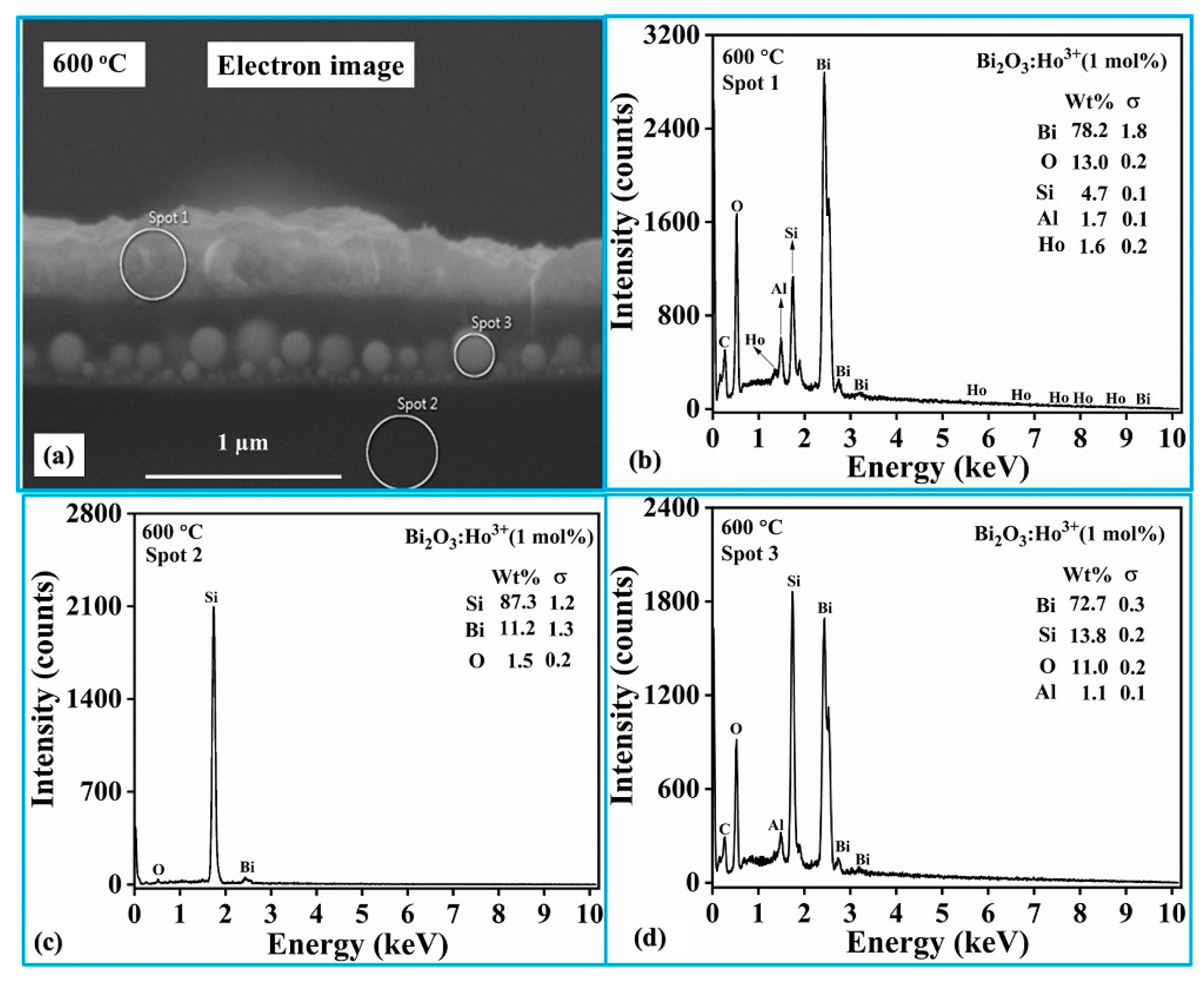
The FESEM cross-section image of the Ho
3+-doped Bi
2O
3 film from T
S = 600 °C is presented in
Figure 7a. To examine the elemental compositions in the three different regions indicated, typically selected spots 1, 2 and 3 represent the coated film surface, substrate (Si) and the Bi
2O
3/Si interface respectively, where the EDS measurements were performed. The elemental analysis of spot 1 and spot 3 exhibited the stoichiometry of the expected Bi
2O
3 product, while the elemental analysis of spot 2 showed a maximum wt.% Si present (as expected) as indicated in the
Figure 7b–d. The presence of a substantial amount of Si in the interface region at spot 3 clearly confirms that interdiffusion of the deposited material and the Si substrate occurred, with the subsequent formation of spherical type of particles. The FESEM image of the Ho
3+-doped Bi
2O
3 film obtained at T
S = 600 °C is presented in
Figure S2a. The EDS spectra of the Ho
3+-doped Bi
2O
3 film with T
S = 600 °C at two distinct regions were obtained as shown in
Figure S2b,c, and are represented as spot 1 and spot 2. The EDS spectra indicate that the two different regions consist of the elements Bi, O, Ho and Si, which confirms that both the regions have nearly the same atomic wt.% of Bi, O and Ho elemental composition.
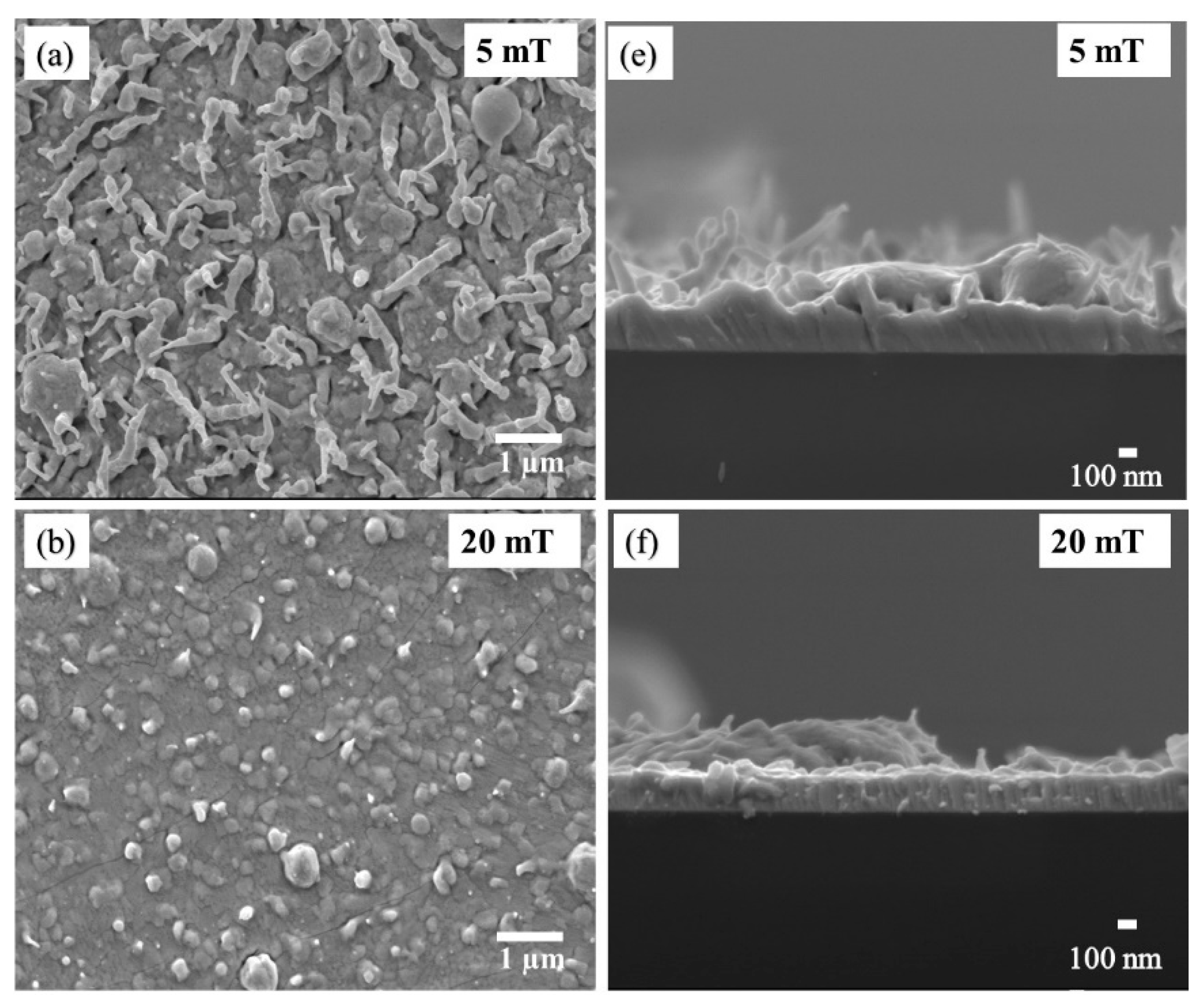
The subtle changes in the surface morphologies of the Bi
2O
3:Ho
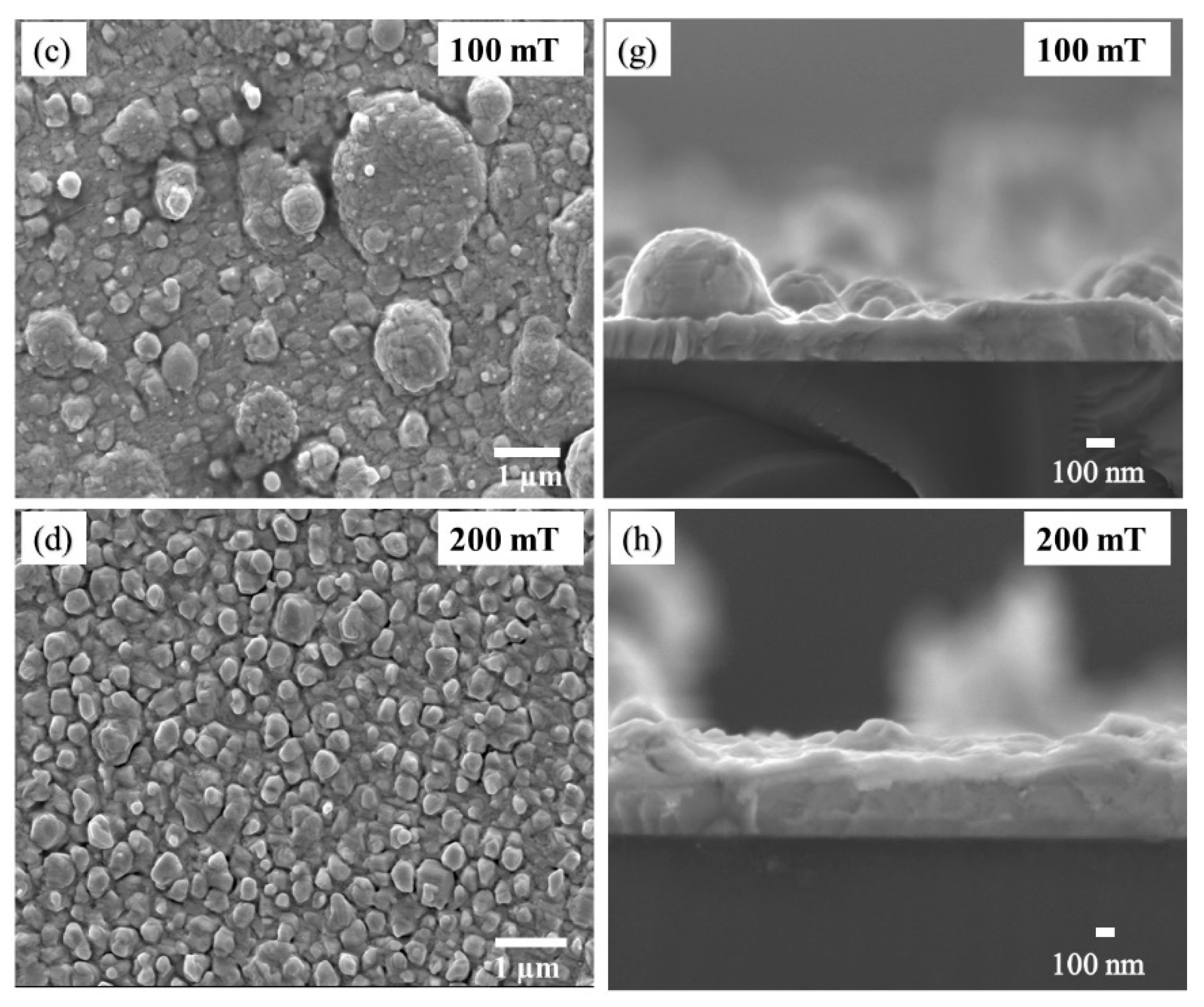
3+ PLD thin films deposited in the different oxygen partial pressures are shown in
Figure 8a–d. The thin film deposited at 5 mT in
Figure 8a indicate uniform sized, needle-shaped grains interrupted by a few spherical shaped grains. The needle-shaped grains disappeared with an increase in oxygen pressure to 20 mT
Figure 8b, and only aspherical shaped grains were observed. At 100 mT oxygen (in
Figure 8c) the small spherical grains became agglomerated, resulting in the formation of larger bigger grains that were randomly distributed on the film’s surface. A further oxygen pressure increase to 200 mT resulted in the formation of finely packed and uniformly sized grains on the surface (see
Figure 8d). FESEM images with two different magnifications of the film obtained at an oxygen partial pressure of 200 mT are presented in
Figure S3. The uniformity of the film is clear.
Li et al. [
61] observed similar behaviour for SrBi
2Ta
2O
9 thin films. At low oxygen pressure (5 and 20 mT), the plume components avoid condensation due to the low probability of these molecules interacting with the chamber oxygen gas molecules and thus reached the substrate surface with relatively high kinetic energy to form the distinct grains observed [
62]. As the oxygen pressure increased to 100 mT, the collision probability among the plume components with the chamber oxygen increased, which decreased their kinetic energy. As a result, the surface diffusion of the atoms slows down, condition which favours grain growth, resulting in a bigger grain size due to agglomeration [
63]. Further increasing the oxygen partial pressure to 200 mT increased the possibility of more frequent collisions between the atoms, decreasing the kinetic energy even more. This reduces the ability of the atoms to move on the substrate surface, which reduces the degree of agglomeration, resulting in better results at a higher temperature [
64,
65]. Ali et al. [
66] also observed similar results during the deposition of thin Y
2O
2S:Eu
3+ films using PLD. The deposition at higher oxygen partial pressure led to nucleation and growth of smaller nanoparticles with less agglomeration. The changes in the surface morphology might also be due to the orientation of the crystal [
67]. The likelihood of this was observed in the XRD result reported in
Figure 2. At 5 mT pressure, the product on the substrate surface was dominated by α-Bi
2O
3 in relation to the non-stochiometric Bi
2O
2.3; when the oxygen partial pressure was increased to 100 mT, the non-stochiometric Bi
2O
2.3 phase dominated; and at the highest oxygen partial pressure (200 mT), α-Bi
2O
3 became the dominated phase when compared to that of the 100 mT oxygen partial pressure.
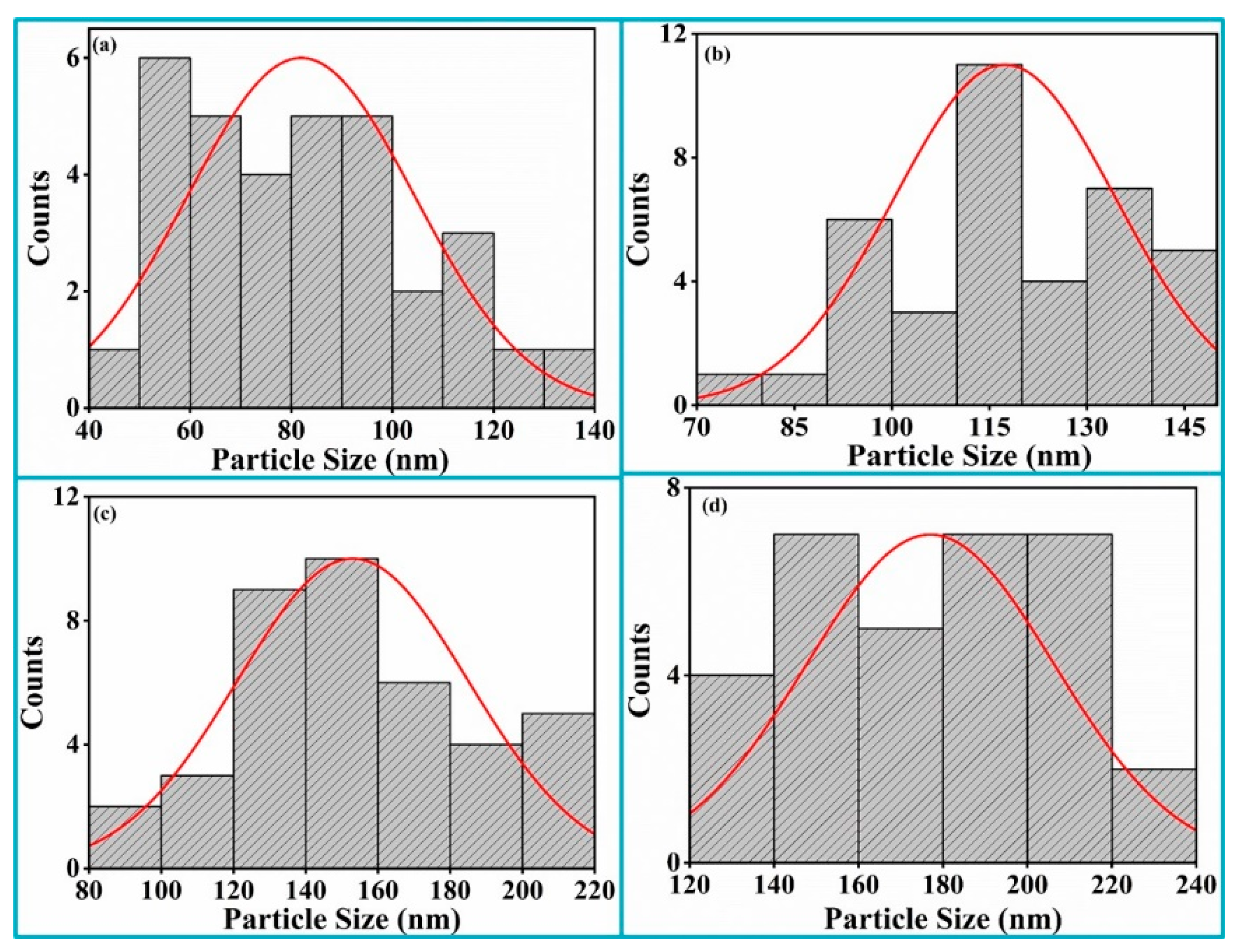
Figure 9 shows the histograms for the particle size distribution and the Gaussian fitting curves of the Bi
2O
3:Ho
3+ thin films deposited in the different oxygen partial pressures. The average particle size was found to be 82 nm for 5 mT, 117 nm for 20 mT, 153 nm for 100 mT and 177 nm for 200 mT. It significantly increased with an increase in the oxygen partial pressure and conformed that an almost uniform particle distribution occurred at the 200 mT oxygen pressure.
The FESEM results were also used to study the film thickness on the substrate surface. This indicated that the average film thickness remained almost constant at 226 ± 10 nm when the oxygen partial pressure was varied between 5 and 20 mT. The film thickness increased to 248 ± 37 and 515 ± 19 nm when the partial pressure was increased to 100 and 200 mT, respectively. The deposition rate was calculated to be 15 nm/min for the 5 and 20 mT oxygen partial pressures. Further increases in the oxygen partial pressure accelerated the film deposition rate to 16.5 and 34 nm/min for 100 and 200 mT, respectively. The increase of the thin film thickness at higher the oxygen partial pressures is therefore attributed to the increase in the deposition rate. At low oxygen pressure, the ablated species have a high kinetic energy, and the mean free path is long and can easily reach the substrate. Some of the incident ablated species with high kinetic energy tend to desorb from the substrate due to the effect of re-sputtering. That leads to a decrease in the deposition rate. With an increase of oxygen pressure, the mean free path of the ablated species becomes shorter, which leads to an increase in collisions between the ablated species and the background oxygen molecules. As a result, they lose some of their partial kinetic energy before reaching the substrate, resulting in an increasing number of adatoms which manifests itself in an increase in deposition rate at higher oxygen pressures [
65,
68]. Zhang et al. [
68] and John et al. [
66] observed a similar result for the Bi
2O
3–ZnO–Nb
2O
5 thin films and BaSnO
3 thin films deposited by the PLD method. The EDS elemental analysis of the Bi
2O
3:Ho
3+ (1 mol.%) films deposited at different O
2 partial pressures with T
S = 400 °C indicated the presence of Bi, O and Ho elements and are reported in
Figure S4.
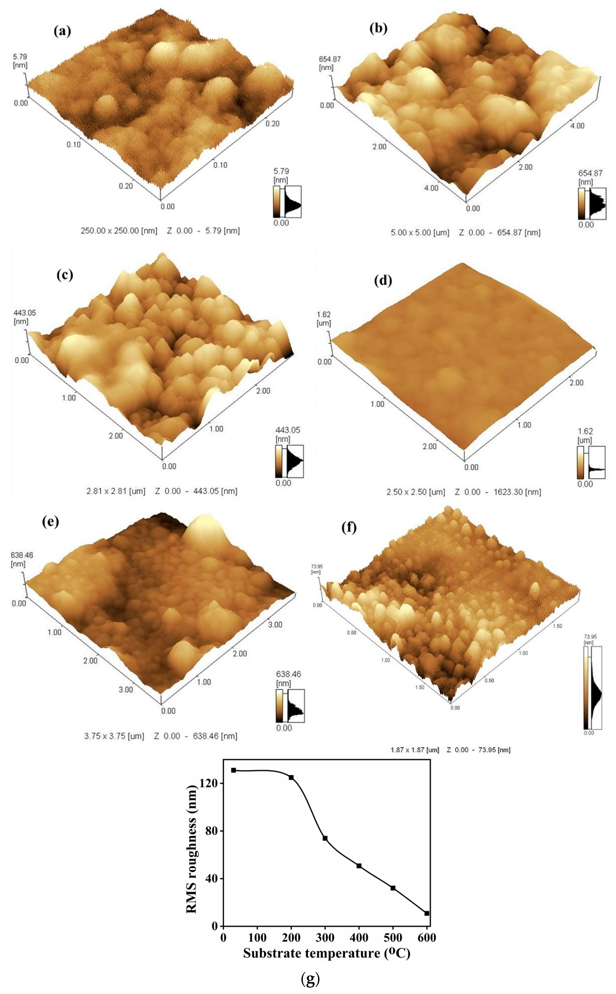
AFM analysis is a power technique to quantitatively measure the nanometric dimensional surface roughness and for visualizing the surface nano-textures of the deposited films. The 3D-AFM images of the Bi
2O
3:Ho
3+ (1 mol.%) films deposited at different T
S in vacuo are given in
Figure 10a–f. The films exhibited agglomerate grains at low T
S (RT, 200, 300 and 400 °C) and decreases in agglomeration at 500 and 600 °C. The plot of the surface root mean square (RMS) roughness values of the films as a function of substate temperature is shown in
Figure 10g. The calculated RMS roughness value decreased with an increase in the T
S: 131.0, 124.9, 73.9, 50.7, 32.1 and 10.8 nm at RT, 200, 300, 400, 500 and 600 °C, respectively. The results in
Figure 10a–d indicate indistinct grain boundaries and very rough surfaces for the thin films produced. At higher T
S the adatoms initiated the formation of more crystalline particles with defined boundaries, resulting in smoother film surfaces. At 500 and 600 °C, however, the number of the adatoms decreased, resulting in a decrease in the RMS roughness value of the film. The reduction in the surface roughness at higher T
S can be attributed to the increase in atom mobility, resulting in improved atom diffusion rates, resulting in atoms reaching their equilibrium positions very easily and quickly [
58]. Both XRD patterns and AFM images of the as-deposited Bi
2O
3 films indicated that the substrate temperature has a significant effect on the crystallite size and the roughness of the film’s surface.
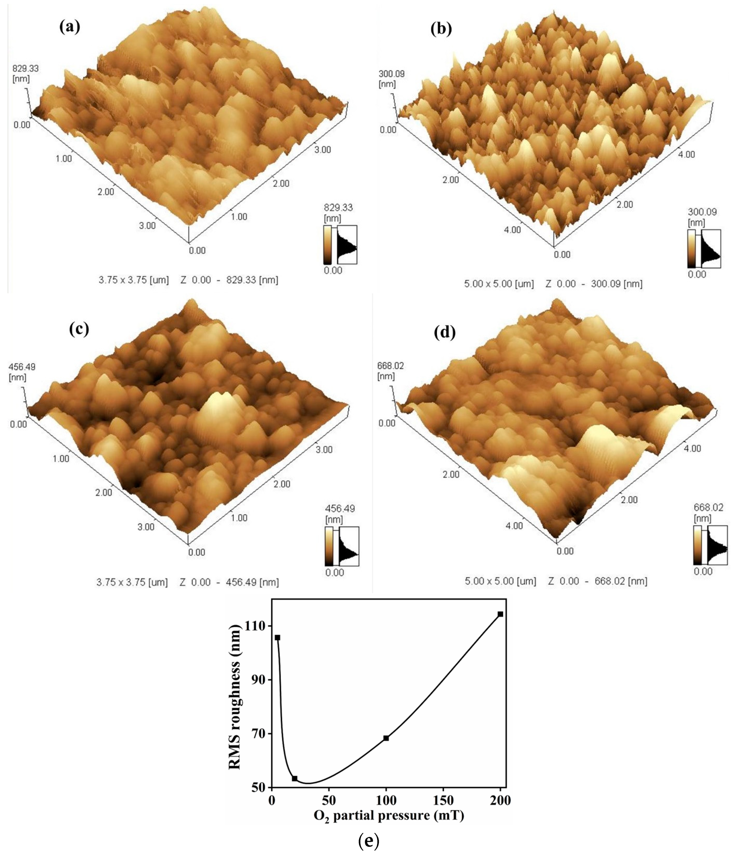
The surface morphologies of the as-deposited Bi
2O
3 thin films as a function of O
2 partial pressures were also investigated by AFM analysis. The AFM images are shown in
Figure 11a–d for the various O
2 partial pressures. The results in
Figure 11b (20 mT) show a thin film with well-defined grain boundaries with small grains. The RMS roughness values were calculated as 105.7, 53.3, 68.3 and 114.4 nm at 5, 20, 100 and 200 mT, respectively. The results in
Figure 11e indicate an initial decrease in the RMS roughness value with an inflection point at 20 mT O
2 partial pressure and then a continued increase in RMS roughness with an increase in O
2 partial pressure.
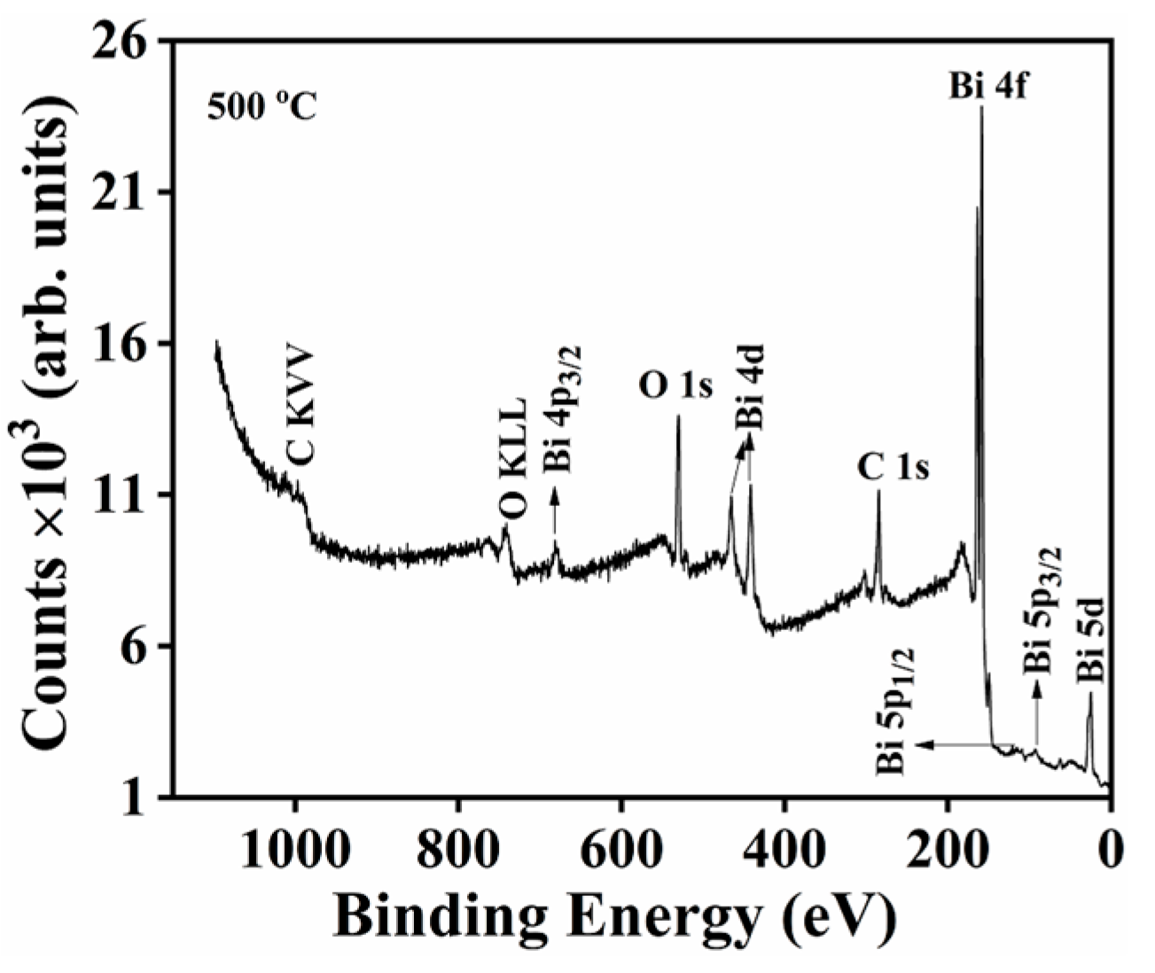
The XPS survey spectrum of a 1 mol.% Ho-loaded Bi
2O
3 thin film obtained at a substrate temperature of 500 °C reported in
Figure 12. The XPS spectrum indicates the presence of Bi (Bi 4f, Bi 4d, Bi 4p, Bi 5p and Bi 5d), oxygen (O 1s) and carbon (C 1s), as indexed in
Figure 12. Interestingly, the spectrum shows no traces of Ho oxide or the metal ion, which can only be attributed to its low concentration, or maybe due to its low atomic sensitivity factor, i.e., 2.469 [
69]. Survey and core-level XPS spectra were corrected for the charge shift using the C 1s peak of adventitious carbon (BE = 284.7 eV), which was used as a reference [
2,
69].
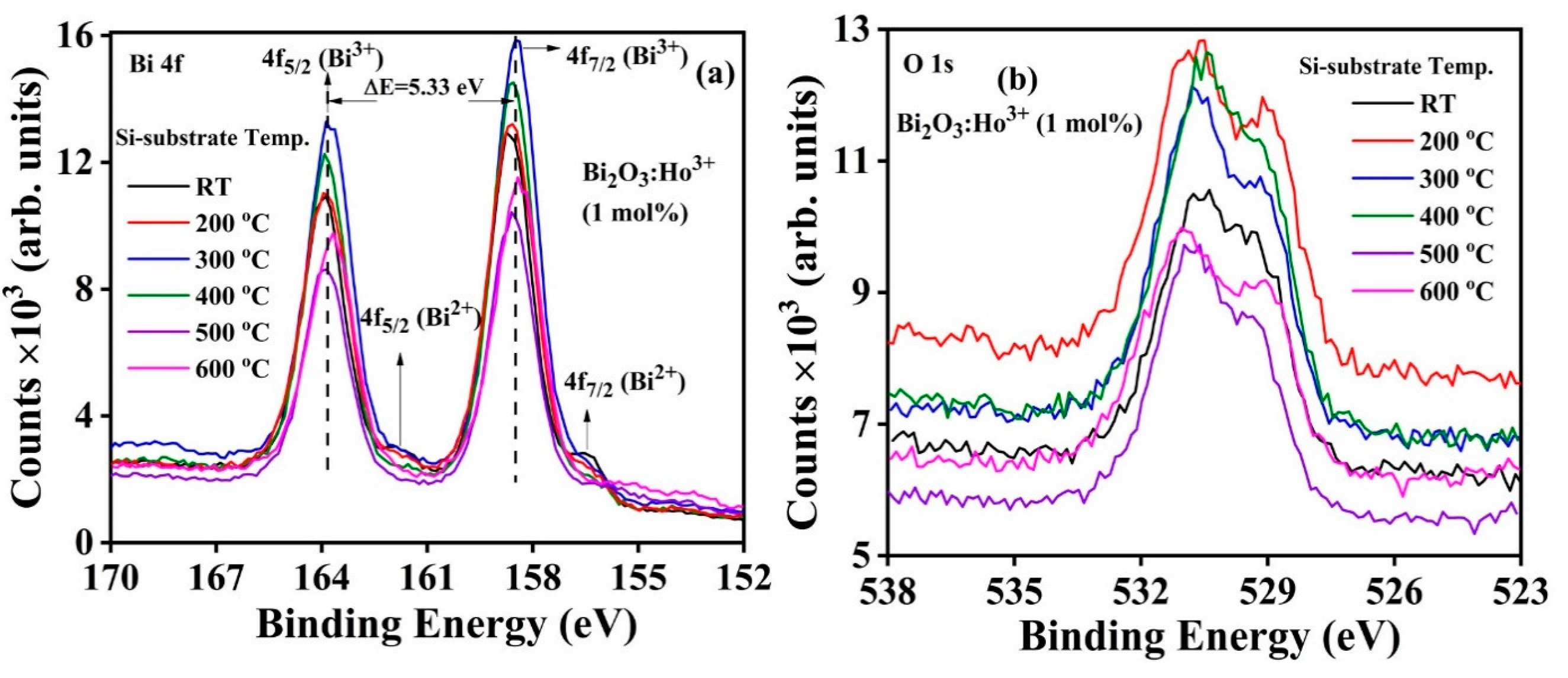
The high-resolution spectra of the different films obtained at the different substrate temperatures show that the Bi 4f
5/2 and Bi 4f
7/2 peaks were separated with a binding energy of 5.33 eV and along with small peaks at the low binding energy side of each peak, as shown in
Figure 13a. The binding energies of the peaks and the corresponding full-width at the half maxima of the peaks (FWHM) are tabulated in
Table 3. No shoulder peaks were observed at 500 °C and the peak was symmetric in nature. The spectra of Bi 4f deposited on the substrate at the other temperatures, however, displayed small peaks on the lower-binding energy side of each of the larger peaks and were asymmetric in nature, suggesting that each peak consists of at least two different peaks. A similar phenomenon was observed for the O 1s high resolution spectra (
Figure 13b).
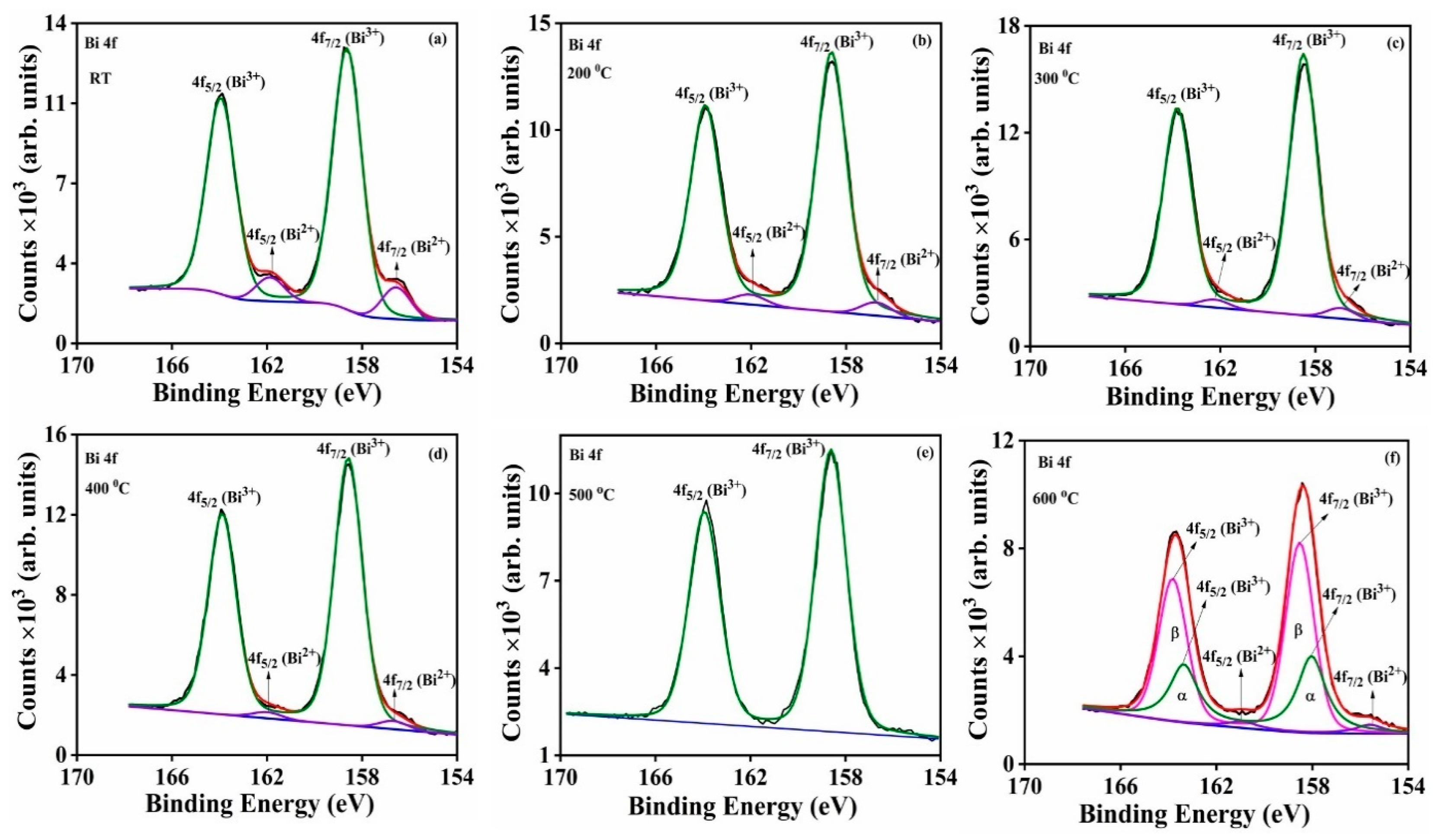
The Bi 4f peak in
Figure 14a–f was deconvoluted into two separate peaks with binding energies equal to 158 ± 0.3 eV and 163.6 ± 0.3 eV, respectively, and those are assigned to Bi
3+ 4f
7/2 and Bi
3+ 4f
5/2, respectively [
69,
70]. The shoulder peaks which appeared at the lower binding energies of 156.2 ± 0.6 and 161.5 ± 0.6 eV are assigned to the Bi
2+ 4f
7/2 and Bi
2+ 4f
5/2, respectively [
71,
72]. The presence of Bi in a lower oxidation state may be due to the presence of oxygen deficiencies within the samples [
71]. The deposited film at a substrate temperature of 500 °C showed only a single oxidation state of Bi (Bi
3+), indicating that this sample is well defined as only α-Bi
2O
3, which correlates well with the XRD results. At 600 °C, there was a mixed phase product (
and β) which was dominated by β-Bi
2O
3 which is also consistent with the XRD results. The results in
Table 4 confirm that the Bi
2+/Bi
3+ peak ratio decreased with an increase of substrate temperature as far as 400 °C and then increased slightly at 600 °C. This is proof that a well-defined α-Bi
2O
3 thin film was achieved at a substrate temperature of 500 °C.
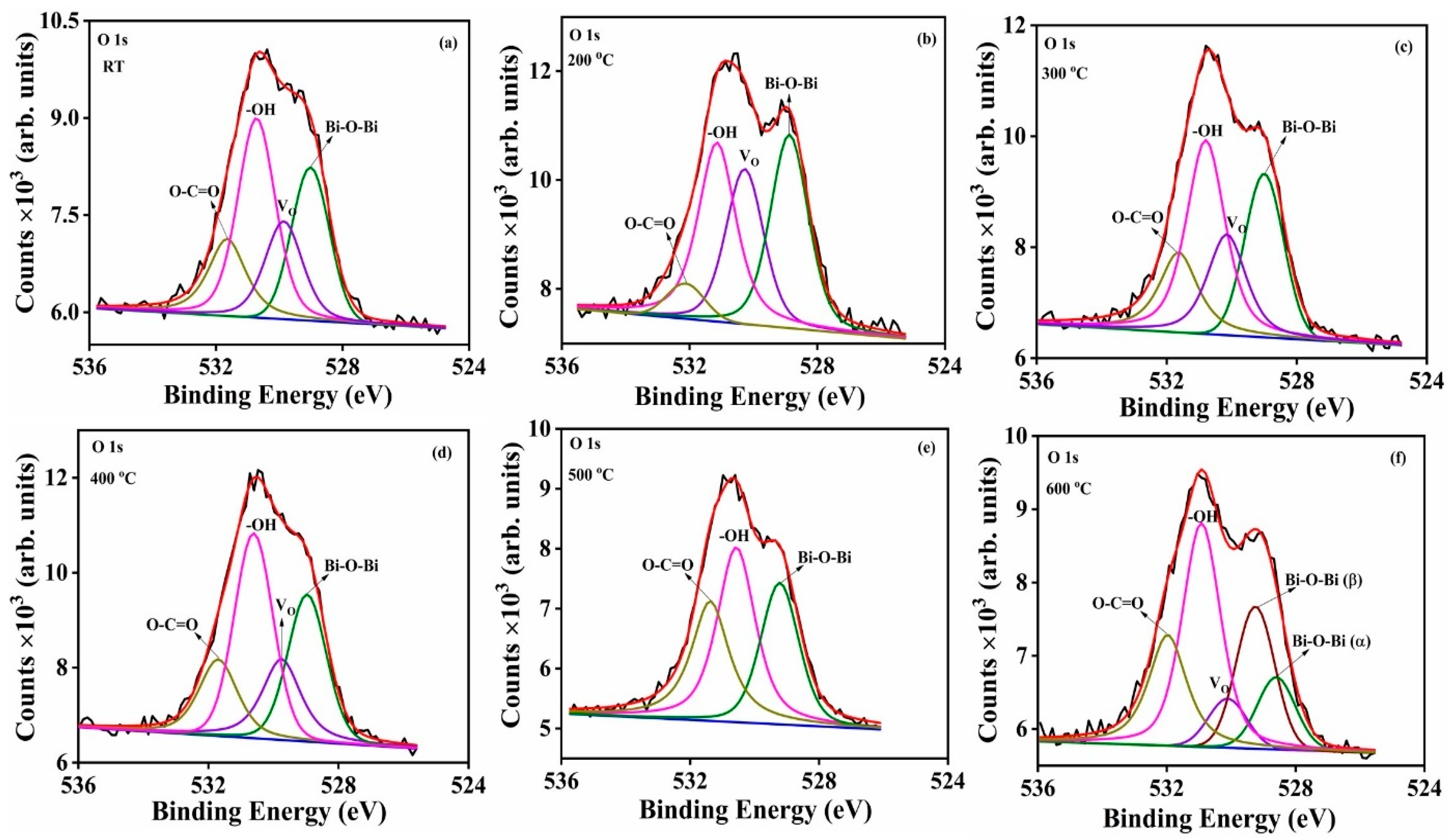
The O 1s spectra for the deposited Bi
2O
3:Ho
3+ thin films, which are reported in
Figure 15a–f, were fitted and the energies of the four peaks were calculated as 529.0 ± 0.2, 530.0 ± 0.3, 530.9 ± 0.3 and 531.7 ± 0.4 eV respectively. These peaks correspond to lattice oxygen (Bi–O); oxygen vacancies (V
O); chemisorbed H
2O or –OH; and O–C=O, respectively [
2]. The V
O may be due to the non-stoichiometric formation of the Bi
2O
3 (i.e., Bi
2O
3−x). The presence of water molecules and carbonate species were possibly due to the samples’ exposure to atmospheric conditions or probably due to the absorption of these species during the product’s atmospheric synthesis [
2]. The T
S 500 °C show three peaks with the absence of V
O, while the T
S 600 °C showed an addition peak with binding energy at 529.5 eV, which is attributed to the lattice oxygen that belonged to the β-phase [
1,
13]. The calculated V
O:Bi–O peak area’s ratios decreased with increasing T
S and are reported in
Table 5.
The high-resolution spectra of Bi 4f and O 1s as functions of different partial oxygen pressures (5, 20, 100 and 200 mT) are shown in
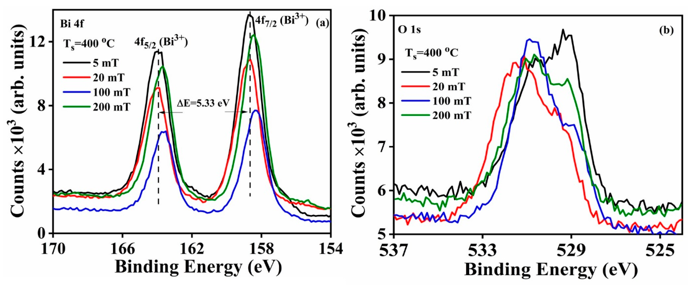
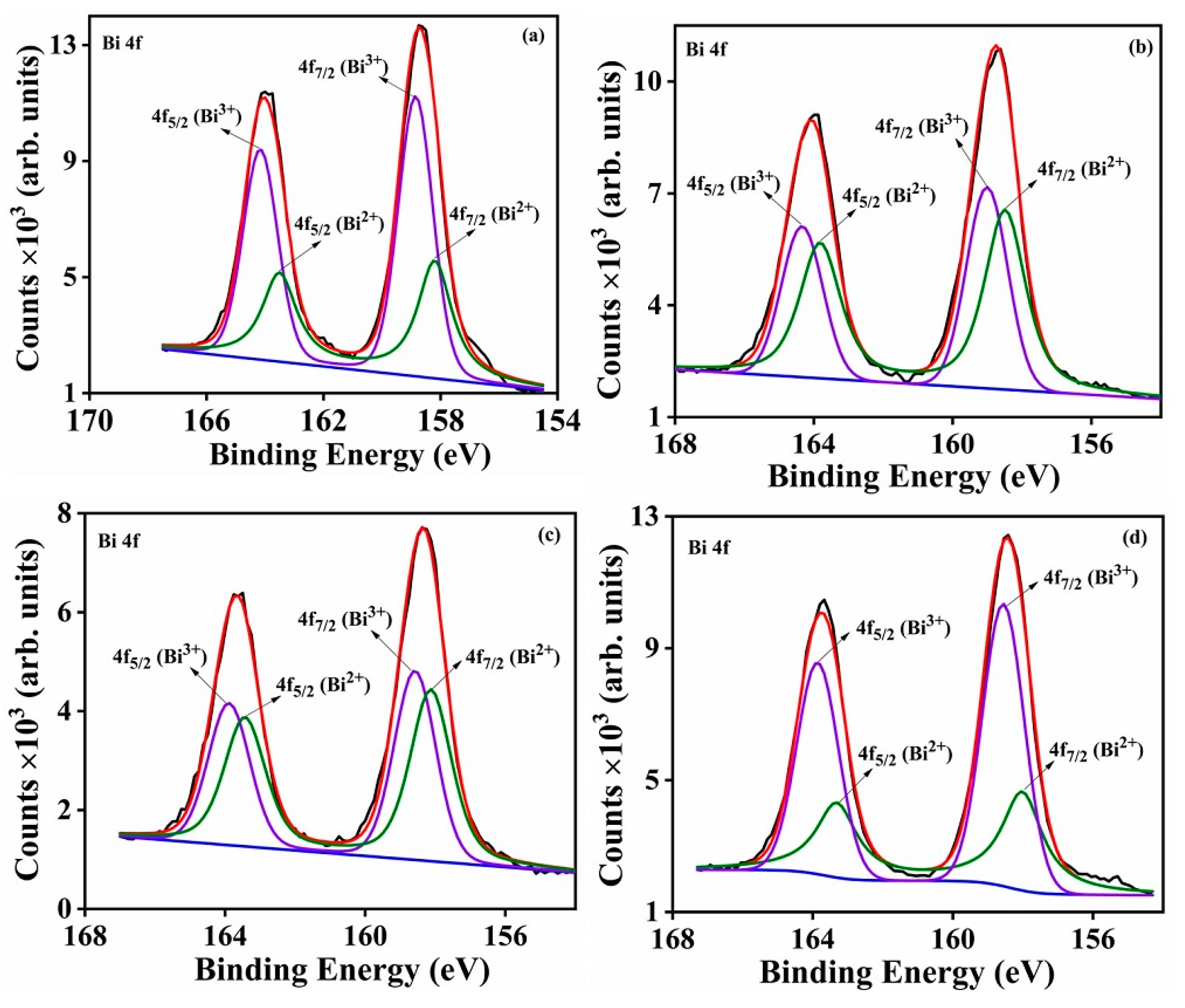
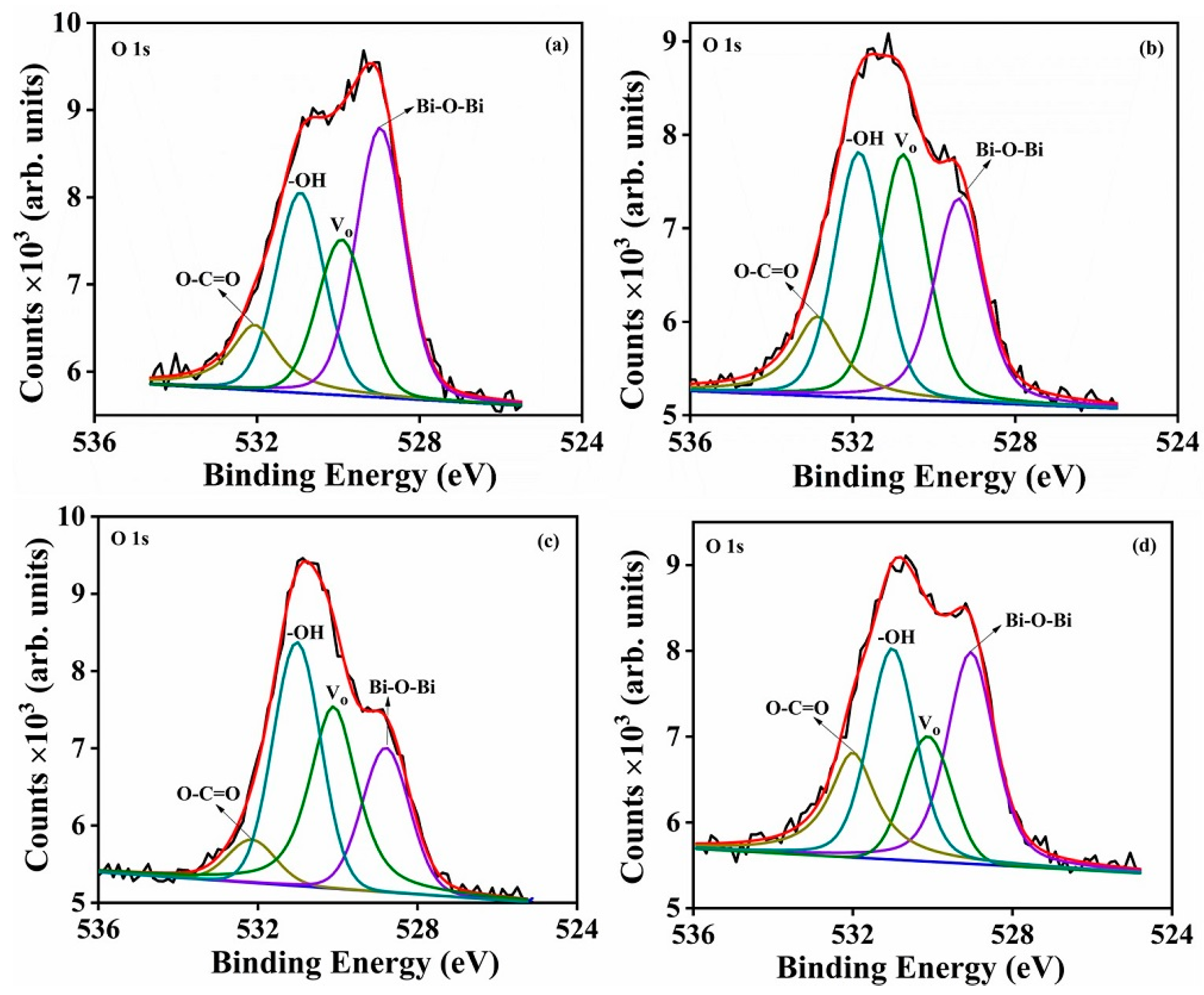
Figure 16a,b. The Bi 4f
5/2 and Bi 4f
7/2 peaks were separated with a binding energy of 5.33 eV. The Bi 4f peak was fitted as two isolated peaks, and their binding energies and corresponding peak areas are summarized in
Table 6. The fitted Bi 4f peaks are displayed in
Figure 17a–d, and the results agree with the presence of Bi in both of its 3+ and 2+ oxidation states in the product [
2]. The calculated Bi
2+:Bi
3+ peak ratios increased up to an O
2 partial pressure of 100 mT, and thereafter decreased with increases in the O
2 partial pressure (
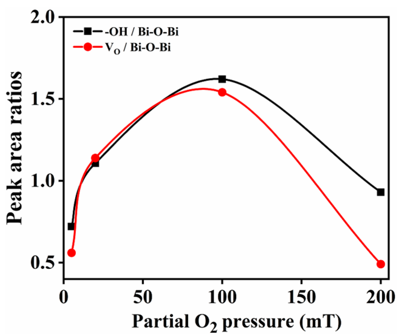
Table 6). The O 1s high resolution spectra were fitted to four isolated peaks and the results are displayed in
Figure 18a–d. The calculated binding energies and peaks areas are tabulated in
Table 7. All four samples exhibited the non-stoichiometric nature of the deposited Bi
2O
3 product. The peak ratios of –OH:Bi–O–Bi and V
O: Bi–O–Bi are plotted as a function of different O
2 partial pressures, which indicated the surface contamination increased till 100 mT and was attributed to –OH to lattice oxygen (Bi–O–Bi) bonding and V
O to lattice oxygen bonding (Bi–O–Bi) (
Figure 19).
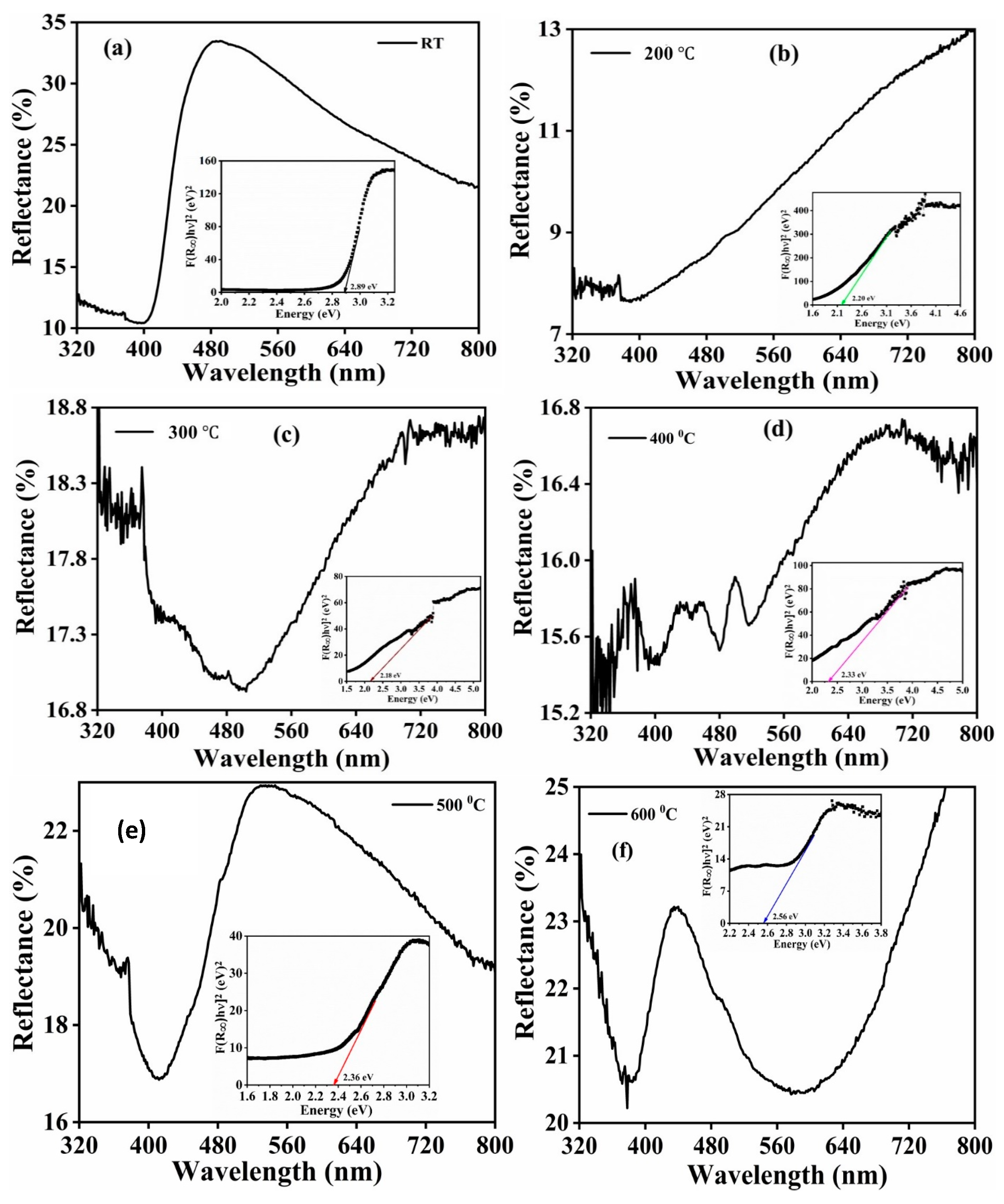
The diffuse reflectance characteristics of the Bi
2O
3:Ho
3+ films deposited at different substrate temperatures are reported in
Figure 20a–f. A sharp absorption peak at 406 nm was observed for the product isolated at RT temperature and is attributed to band edge absorption to the host. The band edge absorption shifted to the higher wavelength side (red shift) with an increases of the T
S till 300 °C (
Figure 20b,c), and thereafter changed to a blue shift with a further increase of T
S (
Figure 20d–f). This temperature increase may induce the formation of localized oxygen vacancies [
73] within the band gap as a result of formation of mixed α- and β-Bi
2O
3 phases. In addition, the small absorption at the 495 nm is assigned to the structural defects [
2,
74].
Figure 20 shows the diffused reflectance spectra oscillated and the lowest reflectance was due to the non-homogeneity of the films and non-uniformity particle distributions, resulting in multiple reflections from the interfaces and to their interference [
11,
75]. The results in
Figure 20 clearly indicate that the reflectance is dependent on the film thickness, and the highest reflectance was achieved for the films grown at the RT that coincided with the thickest film observed.
The optical band gaps of thin films were estimated using the Kubelka–Munk (K–M) model [
1]. The values of the direct optical bandgaps were obtained from the plots of [F(
h
]
2 as a function of energy (h
). The direct allowed band gaps were obtained by extrapolating the linearly fitted regions of [F(
h
]
2 to zero and are shown in the inset of
Figure 20a–f. These calculations indicated that the direct allowed bandgaps for the Bi
2O
3:Ho
3+ thin films were 2.89, 2.20, 2.18, 2.33, 2.36 and 2.56 eV for T
S of RT, 200, 300, 400, 500 and 600 °C, respectively. These values correspond well with those reported previously [
11] and with the 2.85 eV [
1] that was reported the optical band gap for a 1 mol.% Bi
2O
3:Ho
3+ powder. The obtained optical band gap values for T
S of 200 to 600 °C are relatively smaller than the previous reported values for the powder sample, and that may have been due to the high density of structural defects and presence of the hetero α- and β-phases present in the current products.
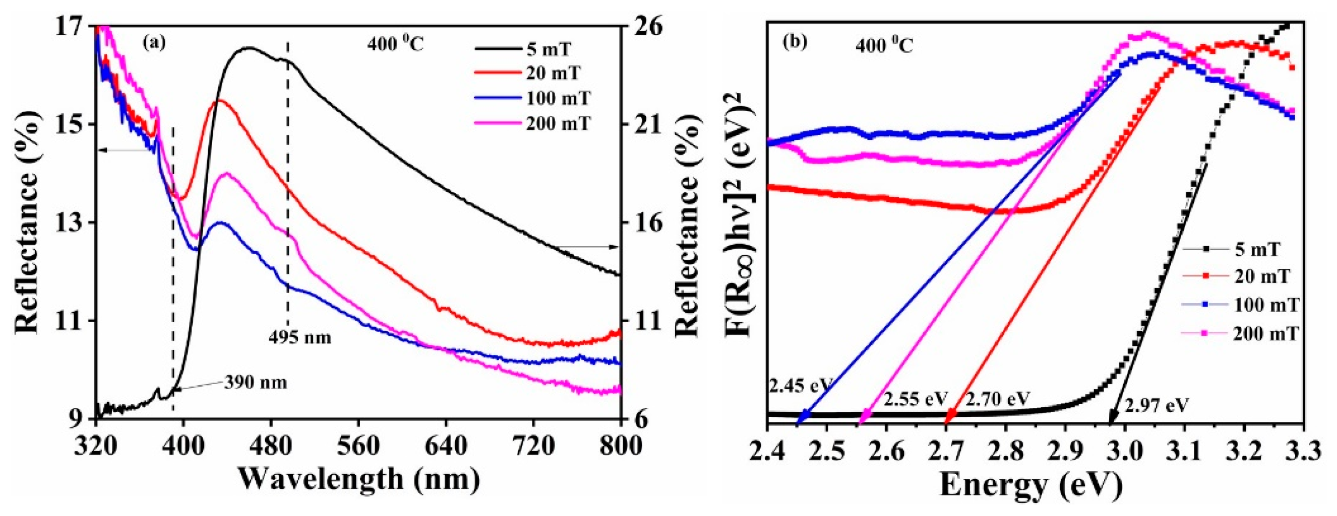
The DR spectra of the Bi
2O
3:Ho
3+ thin films deposited at the different O
2 partial pressures are displayed in
Figure 21a. The band edge absorbance appeared at approximately 390 nm for the 5 mT oxygen partial pressure, and a shift was observed with an increase in the O
2 partial pressure. Additionally, a small peak observed at 495 nm may have been due to the oxygen vacancies in the structure [
1]. The bandgap value decreased up to an O
2 partial pressures of 100 mT and then increased at 200 mT (
Figure 21b). The decrease of the bandgap value was ascribed to the creation of localized states within the band gap due to an increase of the oxygen vacancies until 100 mT [
73]. The increase in the bandgap value at 200 mT may have been due to the reduction of these oxygen vacancies. This indicates that both the α-Bi
2O
3 and a suboxide Bi
2O
2.3 (oxygen deficiency) phase were formed during the Bi
2O
3:Ho
3+ films’ deposition on the Si substrates at 400 °C and in the presence of different oxygen partial pressures (5–200 mT), and this is confirmed by XRD results (see
Figure 2). The variations of bandgap for the thin films are well supported by XRD (
Figure 2) and XPS (
Figure 19) results. The reported bandgap value of stoichiometric α-Bi
2O
3 was ≈2.85 eV [
1,
13].
Figure 2 showed a mixed phase of α-Bi
2O
3 with a strong reflection at 27.3° (α) and the non-stoichiometric/ oxygen deficiency Bi
2O
2.3 phase with a strong reflection at 29.2° (#). The oxygen pressure increase from 5 to 100 mT resulted in the decrease of the strong α-Bi
2O
3 XRD reflection at 27.3°, and the oxygen deficiency phase XRD peak intensity at 29.2° increased, as a result of the increase of the oxygen vacancies in the film [
76]. At 200 mT the stoichiometric XRD peak intensity at 27.3° increased, and the oxygen deficiency phase XRD peak intensity decreased (see
Figure 2) due to the backfilled oxygen atoms occupying the oxygen vacancies, hence a reduction in the oxygen vacancies [
77]. The obtained bandgap values are consistent with previously reported results [
11].
The PL excitation spectra of the isolated Bi
2O
3:Ho
3+ thin films deposited at the different substrate temperatures were obtained at λ
em = 548 nm and are displayed in
Figure 22a. The obtained PL indicated intensity maxima at 360, 419, 450, 466, 473, and 485 nm and are attributed to the
5I
8 3H
5, 3H
6,
5I
8 5G
5,
5I
8 5G
6,
5F
1,
5I
8 3K
8,
5I
8 5F
2 and
5I
8 5F
3 transitions of Ho
3+ ion. The peak at 450 nm appeared to be the strongest excitation peak and corresponds well to previously obtained results [
1,
78]. The
5I
8 5G
6, 5F
1 excitation peak has two peak maxima at 450 and 454 nm. The second peak at 454 nm became more prominent with an increase of the substrate temperature to 600 °C compared to the peak at 450 nm It might be due to the α-Bi
2O
3 oriented crystallographic planes that were reduced at the substrate temperature of 500 °C and partially transformed into the β-Bi
2O
3 phase with a further increase of the substrate temperature to 600 °C, and as a result the oriented crystallographic planes were changed, which is consistent with the XRD results (see
Figure 1). Zhang et al. [
79] studied the optical absorption spectra of MgWO
4:Ho
3+ crystal for light polarizations E
a, b, c, where a,b,c are the orientations in the crystallographic frame {a,b,c}. The main absorption peak at about 448 nm due to the
5I
85G
6,
5F
1 transition of Ho
3+ consisted of two peaks at about 448 and 452 nm due to the stark splitting [
21]. When the light polarization was E
c, the ≈452 nm peak intensity was dominant. For light polarizations E
a and E
b, the 448 nm peak intensity was dominant. The PL emission spectra of all the films deposited at different substrate temperatures and excited at 450 nm are reported
Figure 22b. A broad and highly intense green emission peak was found at 548 nm, and is ascribed to the
5F
4/
5S
2 5I
8 Ho
3+ transition; the relatively weak red emission peaks at 655 and 756 nm are attributed to the
5F
5 5I
8 and
5S
2 5I
7 transitions of Ho
3+ ion [
1]. The variations in the ratio of the emission intensities between the green and red transitions of the Ho
3+ ions may be due to the phonon energy effects. It is well known that Ho
3+ has several meta-stable states which are situated between its
5F
5,
5I
4,
5I
5 and
5I
8 energy levels, and small energy gaps between these state give rise to the cross-relaxation effects which can lead to a high phonon energy effect. This phonon energy will diminish the intensity of the emitted red light, and the weak red intensity emission, compared to the green emission intensity, is well documented [
80]. The intensity of the green emission increased with an increase in substrate temperature from RT to 500 °C (see
Figure 22c) possibly due to improved crystallinity and the formation of the stoichiometric α-Bi
2O
3 product. These results correlated well with those obtained from the XRD and XPS studies. These results indicate that the surface morphology changed, and the RMS results indicated a decrease in surface roughness attributed to the increase of the substrate temperature, which ultimately improved the PL properties. The structural defects and oxygen vacancies also played vital roles in the PL intensity and emission profiles, and these defects acted as luminescence quenchers and/or enhancers [
81]. In the present study the oxygen vacancies acted as a Ho
3+ emission quencher, and the PL intensity increased with the reduction of the oxygen vacancies, which was confirmed from the XPS results. In addition, the maximum PL excitation intensity appeared at 454 nm with an increase in the substrate temperature to 600 °C. The emission maxima with excitation at 450 nm, therefore, appeared lower than those at 500 °C, possibly due to the fact that the emission intensity was measured at a slightly lower value. The broad excitation observed in the 360–420 nm region for the substrate temperature 600 °C indicated the presence of crystal defects, lattice disorders that also contributed the Ho
3+ excitation peaks, which was also evident in the XRD, surface morphology and XPS results. A similar result was observed for the MgWO
4:Ho
3+ crystal [
79].
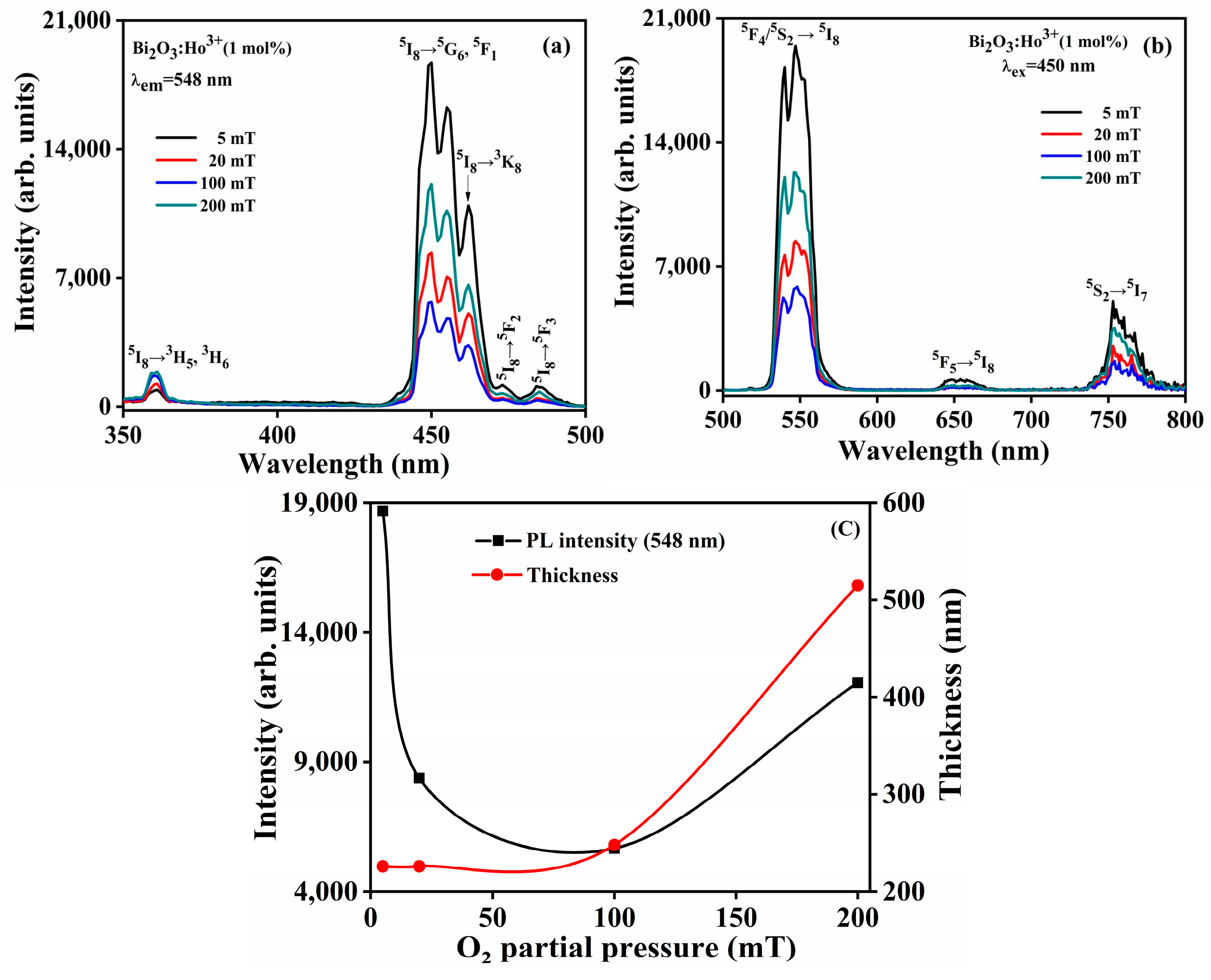
The excitation and emission spectra of the Bi
2O
3:Ho
3+ thin films were studied using the films deposited at constant substrate temperature (T
S = 400 °C) and at various oxygen partial pressures, and the resultant spectra are reported in
Figure 23a,b. It is clear from the results in
Figure 23 that the PL excitation and emission spectra were very similar to those of the films obtained at the lower substrate temperatures (<500 °C (
Figure 22a,b). The results indicate PL intensities were higher for the films deposited at the different oxygen partial pressures (see
Figure 23c), compared to the films created in vacuo, and may be attributed to a decrease in the agglomeration of the particles. The results indicate an initial decrease in intensity with the increase of oxygen partial pressures (5–100 mT), since it depends on the surface morphology of the substrate. At 5 mT (uniform), needle-shaped grains were observed, but the increase of the oxygen partial pressure led to the agglomeration of particles, which ultimately led to a decrease of the PL intensity. At 200 mT the PL intensity increased, possibly due to the uniform distribution and reduction of the agglomeration of the particles on the film surface. That was also confirmed by the formation of fewer oxygen vacancies and surface contamination in the form of –OH, as indicated by the higher PL intensities. The obtained PL results are well consistent with the XRD and XPS results. The decrease in PL intensities in the Ho
3+ transitions in the Bi
2O
3 thin films is attributed to the presence of oxygen vacancies and –OH groups. In the present study, the PL intensity of the Bi
2O
3:Ho
3+ films deposited at the different substrate temperatures in vacuo and different oxygen partial pressures significantly changed with the film thickness, and the obtained results are given in
Figure 22c and
Figure 23c.
Figure 22c indicates that the PL intensity of the 548 nm peak increased with a decrease of the film thickness up to the substrate temperature of 500 °C, and thereafter the PL intensity decreased at the substrate temperature of 600 °C. This is the opposite of what was expected: that a thinner layer would give a lower intensity. Other secondary effects, such as the changes in crystal structure and crystallite orientation, therefore, played more pronounced roles in the increase of the intensity. An increase of the PL intensity at the higher substrate temperature was due to the formation of the mixed α-β Bi
2O
3 phase with the dominated β-Bi
2O
3 phase. Additionally, the value of the texture coefficient in the (
plane of the α-Bi
2O
3 was a minimum (see
Table 1). In
Figure 23c, the PL emission intensity of the 548 nm peak increased with increases of film thickness and with increases in the O
2 partial pressure. The increase of the PL intensity at 200 mT was due to the uniform distribution of the particles, which was well consistent with the texture coefficient in the (
plane of the α-Bi
2O
3 (see
Table 2).

 ,
, 


