1. Introduction
ZrO
2-Sm
2O
3 is an attractive material for many applications, such as: phonic and electronic devices [
1,
2,
3,
4,
5,
6,
7], catalysts [
8], biomedical uses [
9], TBCs (thermal barrier coatings) [
10,
11,
12,
13], and electrolytes in SOFCs (solid oxide fuel cells) [
14].
Thermal barrier coatings built of SDZ (samaria-doped zirconia), deposited on metals, e.g., on gas turbines, are obtained using the APS (atmospheric plasma spray) and EBPVD (electron beam physical vapor deposition) methods. They are manufactured in the form of multilayers that are porous and non-uniform in thickness (even up to 20%) by means of APS. Layers obtained by means of EBPVD are also porous, but this porosity is lower compared to the same layers produced using the APS method. They have a columnar microstructure and consist of grains that can be measured in micrometers. The mechanical strength of the layers is higher when they are deposited by EBPVD due to their lower porosity. Furthermore, multilayers deposited by APS can delaminate as the turbine is switched on and off multiple times due to rapid temperature changes, which will generate thermal stresses in the layer and on the metallic substrate. For this reason, delaminated layers will be rougher when the process intensifies during long-term use. It should be noted that the roughness of the layer can also lead to turbulent gas flow in the laminar boundary layer over the turbine rotor blades [
15,
16]. Consequently, it can cause the rotor to vibrate, which can subsequently lead to turbine failure. The higher the operating temperature, the more intense the delamination process, because higher stresses appear between individual layers of a multilayer, as well as between the multilayer and metallic substrate.
In the case of TBCs, it is important to ensure low operating temperatures for protected metallic materials, such as rotors in gas turbines, which are surrounded by exhaust gases flowing through the turbine at high temperatures, as well as their stability during long-term use.
It is believed that due to the significantly higher activation energy of the tetragonal-to-monoclinic phase transformation in the case of SDZ (i.e., 308.1 kJ/mol) compared to that of YSZ (Yttria stabilized Zirconia) (231.76 kJ/mol), a TBC built of SDZ will demonstrate greater stability at high temperatures than YSZ [
11]. Furthermore, SDZ exhibits significantly lower thermal conductivity λ than YSZ. It should be noted that the higher the temperature of gases flowing through a turbine, the higher its efficiency and also the lower the emission of harmful components (e.g., CO, soot from exhaust gases). Performance goals of the turbine also increase [
14]. The operating temperature of modern gas turbine varies from 1300 to 1400 °C.
In order to simultaneously ensure that coatings exhibit low thermal conductivity and good mechanical strength, they should be non-porous and nanocrystalline with an appropriate concentration of components stabilizing ZrO
2. These components should have larger atomic (ionic) radii and greater mass than the Zr
4+ ions present in matrix. For example, the ionic radius of Sm
3+ is larger than Zr
4+ (around 100 and 80 pm, respectively), but Zr
4+ and Y
3+ have similar radii [
1]. The atomic mass of Zr is equal to 91.22 u, whereas Sm is 150.36 u. For this reason, the aforementioned thermal conductivity of SDZ is lower than YSZ. The larger ions with greater weight inhibit lattice vibrations and thus phonon transport is slowed down. Phonon transport through amorphous intergranular boundaries is retarded due to the different length of bonds between atoms in amorphous and crystalline structures. As previously mentioned, the volume content of intergranular boundaries increases when grains decrease and, for this reason, the thermal conductivity of materials with such a structure also decreases.
In the case of layer electrolytes for solid oxide fuel cells (SOFC), it is important that they are non-porous and nanocrystalline. Porosity is unfavorable as it enables easy O2 diffusion from the cathode in contact with air to the anode, where fuel is supplied. This, in turn, decreases the O2− ion diffusion stream. Combustion of fuel in oxygen (O2) does not generate free electrons and thus lowers the efficiency of the cell. Only combustion of fuel in O2− leads to the formation of these electrons, which can then conduct an electrical current through the external metallic circuit outside the cell.
Furthermore, in the case of electrolytes, thermal stresses will focus on pores (Cook–Gordon mechanism). These thermal stresses result from, among other things, differences in the thermal expansion coefficients of the electrolyte and electrodes. The stresses are also generated during quick heating of the cell after it is switched on and rapid cooling after it is turned off. They can lead to the formation of cracks throughout the electrolyte, which will result in avalanche transport of O
2 from the cathode to the anode and, as a consequence, destruction of the cell. Small grains in electrolytes also lead to easier O
2− ion diffusion in a looser structure of amorphous intergranular boundaries, the content of which increases as grain size decreases [
17].
For this reason, ionic conductivity of nanocrystalline electrolytes is a few orders higher than that of microcrystalline electrolytes. Therefore, it is possible to significantly reduce the operating temperature of fuel cells with such electrolytes and use significantly less expensive materials for other cell elements. In this way it is also possible to reduce operating costs of the cell and thus reduce the costs of generating electricity. It should be noted that current commercially available YSZ electrolytes are manufactured by powder sintering at 1450 °C. They are non-porous, but have a microcrystalline microstructure, even when the initial size of the powder grains was in the order of nanometers [
18]. Such electrolytes operate effectively only at temperatures around 1000 °C. Furthermore, there are problems with finding electrode materials that will not react with the electrolyte at such a high temperature. Products of these reactions have disadvantageous electrical parameters and therefore electrodes must be built from materials that do not react with the electrolyte. It is known that properties of materials (including electrical properties) depend on their chemical compositions, microstructures, and structures and all of that will be different in the case of products of electrolyte/electrode reactions compared to the initial electrolyte and electrodes. Unfortunately, such materials are expensive. Due to the above-mentioned considerations, finding a solution to the problem is not expected, despite the financial resources earmarked for SOFC development.
It seems that this problem can be solved by manufacturing non-porous nanocrystalline electrolytes (e.g., YSZ) or composite electrolytes (e.g., YSZ/SDC or some other chemical composition) for operation in the temperature range of 600–800 °C [
19]. The ionic conductivity of these electrolytes in this temperature range will be similar to that of polycrystalline YSZ at 1000 °C. Attempts at manufacturing these new materials for electrolyte purposes by means of PVD [
20,
21,
22,
23] and sol-gel [
24] methods have not been successful. So far, PVD methods admittedly allow for obtaining materials built of nano-sized grains, but they are porous and hence not useful for this purpose. Meanwhile, layers obtained by the sol-gel method are nanocrystalline at the stage of their drying and preliminary firing. However, they are also porous and contain cracks. Removal of these defects requires heating such layers to about 1450 °C. They then become non-porous, but microcrystalline, i.e., the same as the materials manufactured by powder sintering [
18].
The purpose of this work is to obtain non-porous nanocrystalline ZrO
2-Sm
2O
3 layers by means of MOCVD using Zr(tmhd)
4 and Sm(tmhd)
3 as reactants. It is expected that application of MOCVD controlled by mass diffusion to the substrate will allow for obtaining layers with predictable chemical compositions based on the molar content of the reactants. In this process, the preliminary concentration of reactants adsorbed on the substrate surface (and later the layer) will be close to zero due to their high rate of reaction. Hence, competition between adsorbing reactants during the synthesis process will not occur. This competition is only possible when the MOCVD (CVD) process is controlled by the surface reaction rate [
19,
25,
26,
27] (in such a case, the process is realized at lower temperatures compared to the processes controlled by mass diffusion to the substrate).
3. Results and Discussion
First, all obtained samples were visually observed. The high transparency of quartz glass substrates enables easy and quick estimation of the layer thickness and its distribution. Moreover, it allows for determining if homogeneous nucleation took place during layer synthesis resulting in the growth of porous layers. In this process, porous powders are formed (their chemical composition is the same or close to that of the synthesized layer). As previously mentioned, they can settle on the top surface of the film as a porous layer that is visible from light scattering. The following factors favor homogeneous nucleation: high reactant concentration in the gas phase, high temperature of the reactants and turbulent gas flow. When laminar gas flow is maintained during the synthesis process, then heat exchange between the substrate and gases is realized only by slow thermal conductivity, i.e., the transport of phonons in a gaseous thermal layer above the substrate, in which there is a temperature gradient Δ
T =
TS −
T∞, where:
TS—the substrate temperature,
T∞—gas temperature at the inlet of the CVD (MOCVD) reactor [
19]. Its thickness depends on the gas flow rate in the reactor and significantly depends on the gradient of static gas pressure, which follows Bernoulli’s equation. The larger this gradient is, the higher the linear gas flow rate, the smaller the thermal layer thickness and the better the laminar gas flow stabilization. As mentioned above, due to gas viscosity, their flow rate at the substrate is zero and thus the static gas pressure and its gradient is measured just above the substrate. In the CVD process, the layer synthesis is controlled by the surface reaction rate at low temperatures. It includes following stages: adsorption of reactants, their activation, their reaction, their diffusion to the substrate (layer) surface, and desorption. Each of these stages can be the slow and control the layer growth. In the CVD process controlled by the surface reaction rate, the atomic content of components of the layer is different from the atomic content of components in the gas phase. While, in the process controlled by the diffusion of reactants to the substrate (when the synthesis temperature is higher), the reactant concentration
pi(s) on the substrate is close to zero (
pi(s) ≈ 0). Due to high temperature of the process, amount of reactants is small and therefore competition in adsorption between reactants cannot occur. For this reason, it is possible to obtain a correlation between the molar ratio of reactants supplied to the reactor and the molar ratio of solid products in the deposited layer (the atomic ratio in obtained layers and in gas phase can be maintained) [
19,
25,
26,
27]. If the CVD process is realized under reduced pressure, then the reactant concentration is lower and process can be controlled by the diffusion of reactants to the substrate at lower temperature. Then it is also easier to maintain laminar gas flow in the CVD reactor and, as consequence, to obtain uniform in thickness layers on large substrates [
16].
It should be noted that when the synthesized layers are non-porous and contain nano-size grains, the layers are visually transparent. When the grains are bigger and pores are present, light scattering is possible and, as a consequence, an opaque layer will be observed. Lights scattering can also occur in microcracks that form on the grain boundaries in the case of polycrystalline layers containing large grains and exhibiting high anisotropy in the value of the thermal expansion coefficient in different crystallographic directions, and low mechanical strength. The formation of these microcracks is the result of significant stresses at the grain boundaries in the layers, as well as a decrease in tensile strength of ceramic polycrystals as the size of the grains increases (this dependence is exponential and follows Weibull’s theory and the Cook–Gordon (C-G) mechanism of crack propagation in brittle materials). The magnitude of thermal stresses at the grain boundary can be estimated from the equation
where: σ
(g,b)—stresses at the grain boundary (
g,
b); α
1; α
2—thermal expansion coefficients on the surface of grains 1 and 2 forming this boundary;
E—Young’s modulus of the layer; ν—Poisson’s number; Δ
T—difference between the synthesis temperature and the ambient temperature.
When α1 > α2, then tensile stresses will occur on the surface of grain 1 during layer cooling and comprehensive stresses will take place on the surface of grain 2. In the case of layer heating, comprehensive stresses will be present on the surface of grain 1 and tensile stresses will occur on the surface of grain 2. When the magnitude of tensile stresses becomes greater than the boundary strength of these stresses, cracks will form at the boundary.
Selected samples were tested using a scanning electron microscope equipped with an EDS analyzer and then subjected to X-ray diffraction studies.
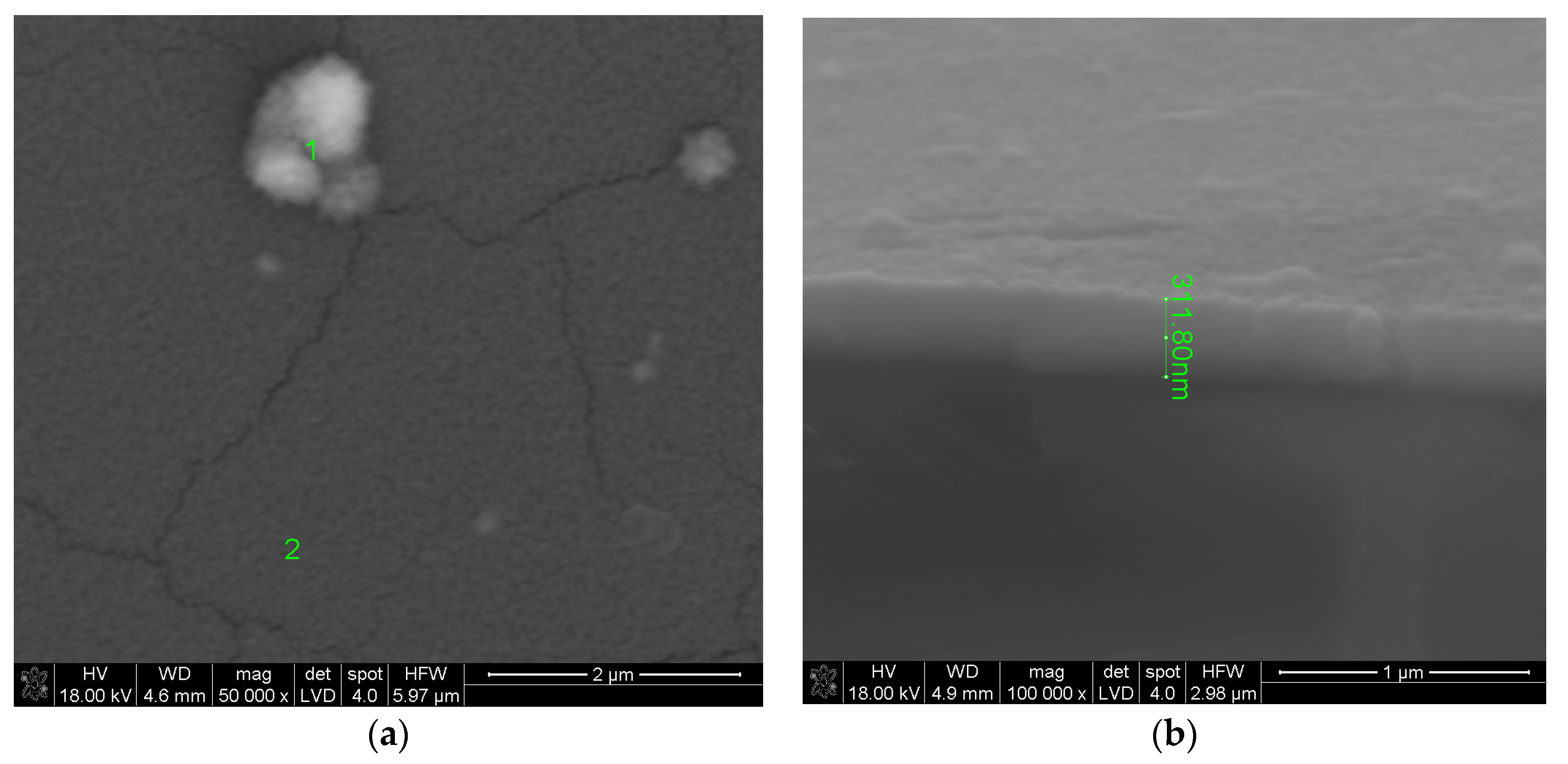
Figure 1 shows the surface of the layer synthesized at 550 °C for 20 min. The molar percentage of Sm(tmhd)
3 was approximately 22.75%. On the layer surface, fair and dark areas, as well as cracks are visible. These cracks were formed during sample breaking for microscopic tests. The fair areas are aggregates of a large number of crystalline grains about 600 nm in size. These aggregates were probably formed on convex fragments of the substrate, i.e., where fragments of incompletely melted quartz sand have remained [
26]. Due to the large convexity of the substrate surface at this location, where the atomic energy of the substrate is higher than the energy on a flat or concave surface due to the lower coordination number (C.N.), nuclei of the layer growing in this location are formed more easily, because their activation energy is lower [
26]. At the dark area, where a larger amount of the amorphous phase is present, a large number of crystallites, single or consisting of a few grains, are visible. The diameter of single crystallites is about 60 nm. EDS analysis presented in
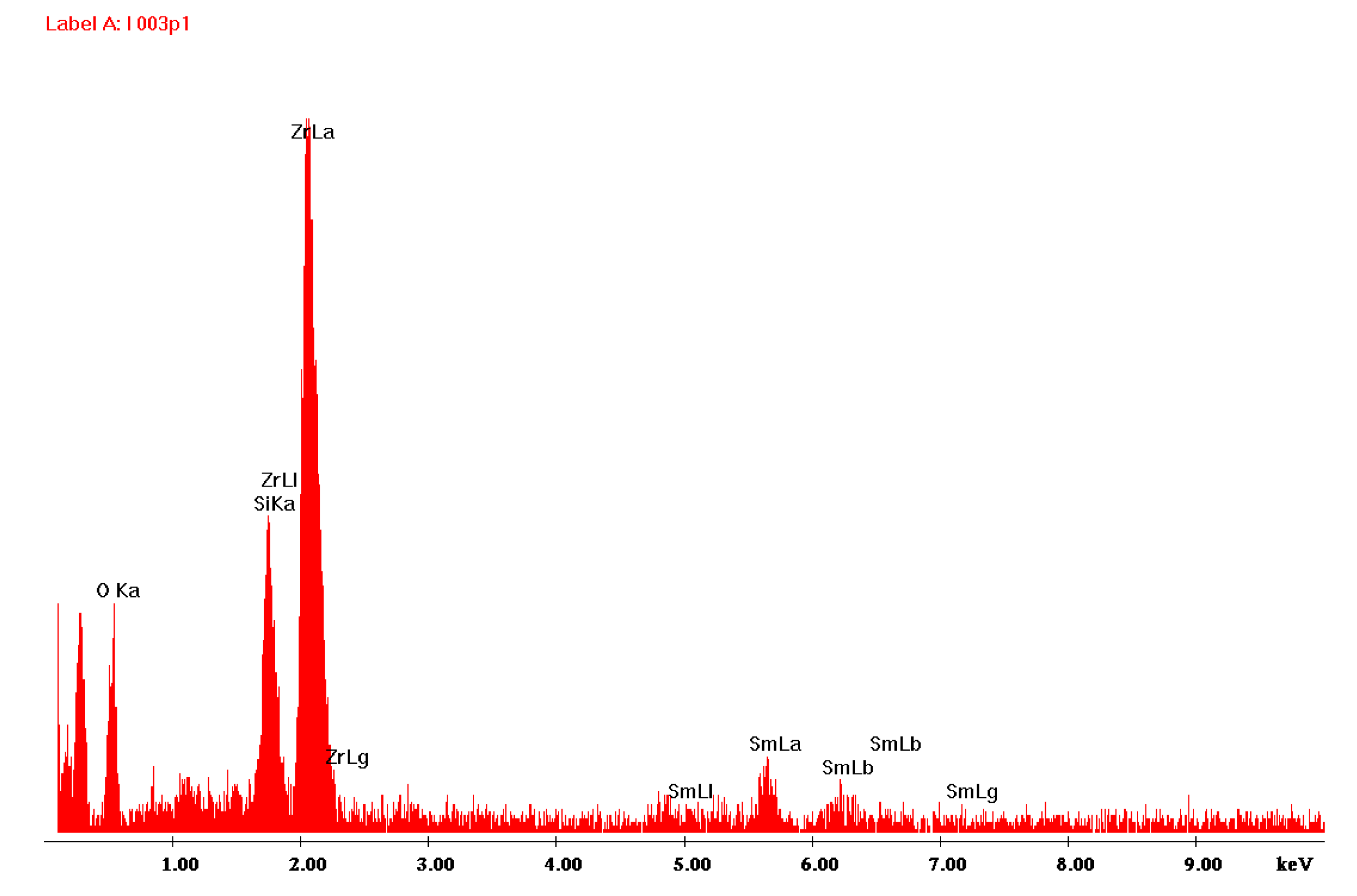
Figure 2 for point 1 (brighter area in
Figure 1) suggests that the amount of Sm
2O
3 in the layer indicated by this point is lower compared to the Sm
2O
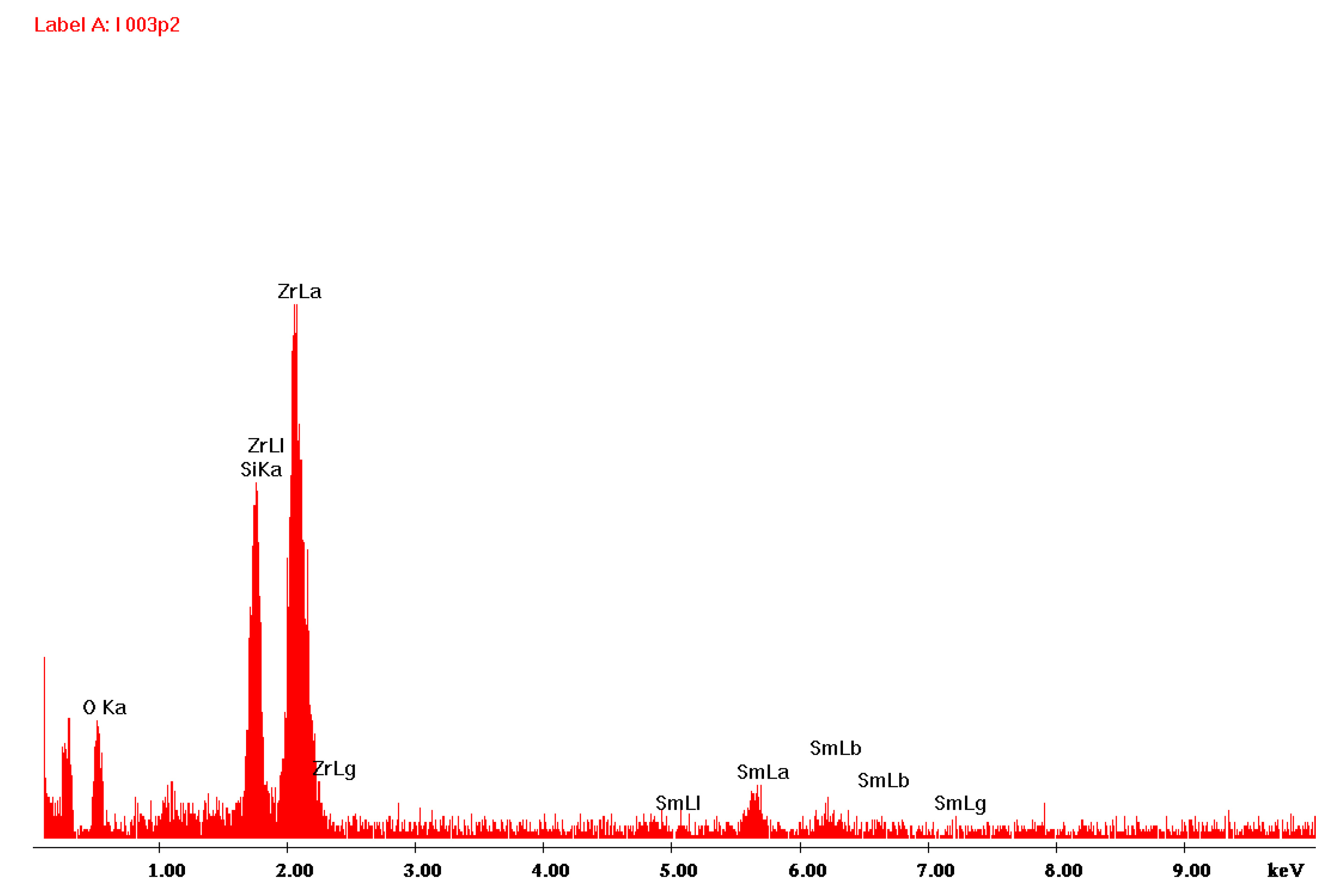
3 content present at point 2, the EDS analysis of which is shown in
Figure 3 (darker area in
Figure 1). The volume percent of the crystalline phase is higher at point 2 than at point 1. Moreover, the more crystallized layer is thicker due to the presence of a substrate defect in the form of its convexity, on which the coordination number of atoms is lower compared to a flat surface. For this reason, the surface energy at this location is greater than that same energy on a flat surface. Hence, nucleation of the layer in these substrate regions and further nuclei growth will occur more easily, because it will lead to a more significant decrease in the energy of a convex surface than in the case of a flat surface without the presence of unmelted sand fragments.
Numerous cracks in the layer presented in
Figure 1, generated during preparation of the sample cross-section for microscopic observations, indicate that the layer thickness is greater in more crystallized places compared to less crystallized ones. Therefore, their mechanical strength is lower than in the case of thinner layers. According to Weibull’s theory, there is a lower probability of the size of a crack becoming critical for a given stress in thinner materials as opposed to thicker ones (exponential dependence).
From
Figure 1b it follows that the layer thickness is equal to about 312 nm. Pores are not present in the layer. The cross-section of this layer with EDS line scan analysis is shown in
Figure 4. EDS line scan analysis (
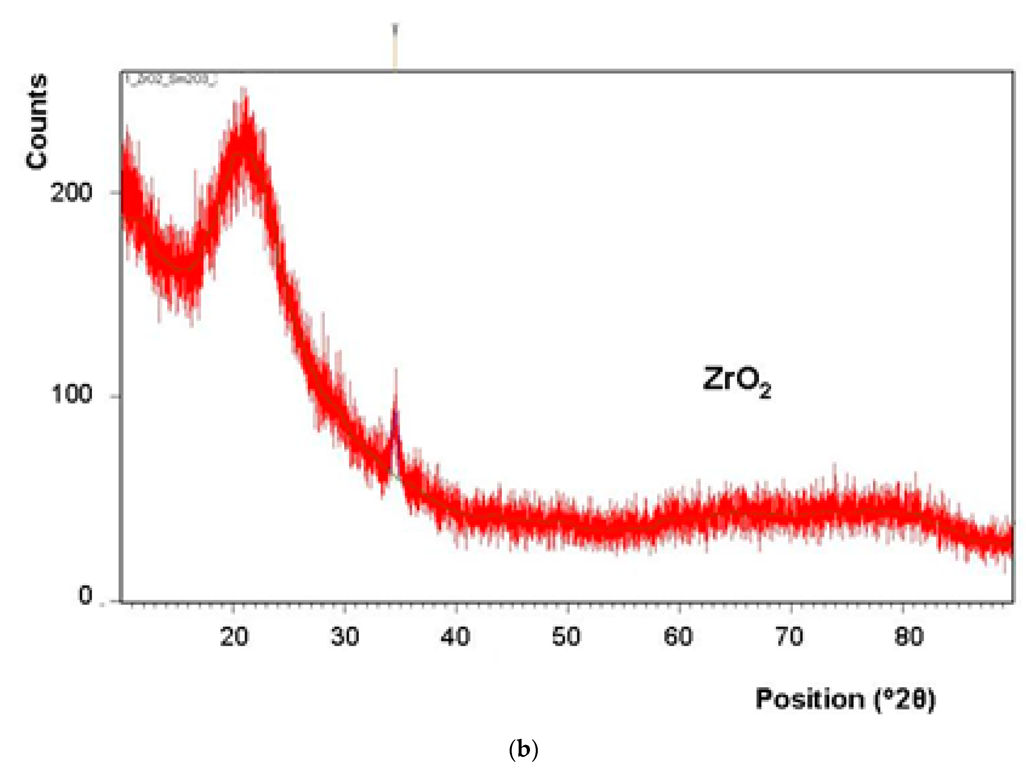
Figure 4) confirms the presence of both Zr and Sm in the layer. Results of X-ray diffraction analysis are illustrated in
Figure 5.
Results of X-ray diffraction analysis (
Figure 5) confirm the presence of a crystalline phase in the layer synthesized at 550 °C, as well as at 500 °C. However, the content of this phase appears to be higher in the layer deposited at 550 °C.
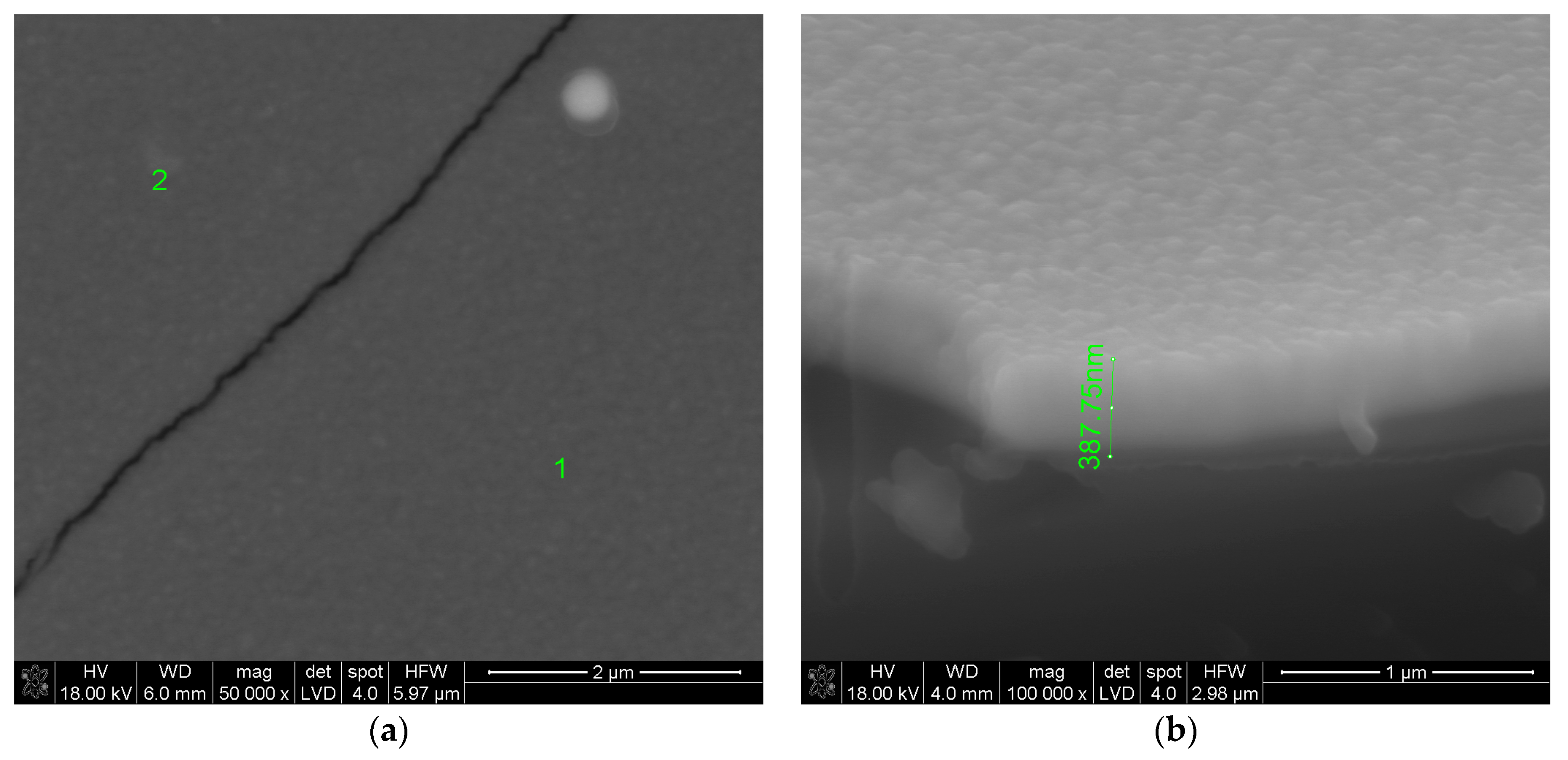
The surface of the layer synthesized at 500 °C is presented in
Figure 6a. The mass of the reactants (Zr(tmhd)
4 and Sm(tmhd)
3) was 1.5 times greater than in the case of the sample shown in
Figure 1. The synthesis time of the layer was 30 min. (1.5 times longer than the synthesis time of the sample presented in
Figure 1).
Figure 6 indicates that the layer is non-porous and less crystalline than the layer presented in
Figure 1. A single aggregate consisting of small grains is also visible. The size of this single aggregate is approximately 300 nm and the size of a smaller grain included in it about 50 nm. It seems that visible lighter and darker areas contain greater and lower amounts of the crystalline phase, respectively. However, the crystallite size is smaller than those presented in
Figure 1 and more uniform in size, particularly in lighter areas.
Furthermore, from
Figure 6b it follows that the layer thickness is only ~388 nm. Therefore, its growth rate was slower than the growth rate of the layer shown in
Figure 1 (even though the weight of the reactants was 1.5 times greater). If this layer was synthesized at 500 °C with the same molar content, but the weight of the reactants was the same as in the case of the layer shown in
Figure 1, its thickness would be approx. 259 nm. Thus, it follows that with 22.75 mol.% Sm(tmhd)
3 and an increase in the synthesis temperature from 500 to 550 °C, the growth rate of the layer increased by 22%. The growth rate increased at 500 °C, because a larger amount of the precursor was used. When the mass of the precursor is greater, the gas flow is more saturated with its vapor and with the same or longer deposition time, even if deposition temperature is 50 °C lower, the growth rate is higher, because the precursor partial pressure was increased.
Table 1 contains the EDS analysis results obtained at point 1 marked on the surface presented in
Figure 6.
The data presented in
Table 1 indicates, that the molar percentage of Sm
2O
3 at this point (where the crystalline phase content is higher) is 9.79%. It should be noted that, if Sm(tmhd)
3 reacted completely, the molar percentage of Sm
2O
3 in the layer would be 11.35%. Results obtained from EDS analysis at point 2 are listed in
Table 2.
Table 1.
Quantitative EDS analysis results obtained from point 1 on the surface of the sample presented in
Figure 6 (only for Zr and Sm).
Table 1.
Quantitative EDS analysis results obtained from point 1 on the surface of the sample presented in
Figure 6 (only for Zr and Sm).
| Element | Weight (%) | Atomic (%) |
|---|
| Zr | 42.88 | 16.78 |
| Sm | 15.35 | 3.64 |
Table 2.
Quantitative EDS analysis results obtained from point 2 on the surface of the sample presented in
Figure 6 (only for Zr and Sm).
Table 2.
Quantitative EDS analysis results obtained from point 2 on the surface of the sample presented in
Figure 6 (only for Zr and Sm).
| Element | Weight (%) | Atomic (%) |
|---|
| Zr | 42.78 | 16.86 |
| Sm | 16.06 | 3.84 |
Figure 6 shows that the layer is darker at point 1 than at point 2, which means that there should be greater amorphous phase content and therefore a greater molar percentage of Sm
2O
3. Data presented in
Table 2 confirms this (the molar percentage of Sm
2O
3 is higher and equal to 10.79%). Data from
Table 1 and
Table 2 also indicates that the Sm
2O
3 segregation process could occur in both the crystalline and amorphous phase at such a low layer synthesis temperature. This seems to be possible, because the substrate temperature is higher than the temperature of reactants in the CVD (MOCVD) process. Initially, particles of gaseous reactants are adsorbed on the substrate surface and subsequently on the layer surface. Then the reaction products are grown on this surface in the form of single atoms or several-atomic clusters. As a result of a surface diffusion, these atoms (clusters) are continuously distributed over the surface of the substrate (layer) [
19].
Ion segregation of rare earth dopants at grain boundaries in ZrO
2 seems to be advantageous in the case of electrolytes (the number of anionic vacancies at these boundaries is increased, thereby increasing the ionic conductivity), as well as in the case of thermal barriers (the possibility of phonons scattering on those associated with the presence of cations increases along with the amount of oxygen vacancies). Thus, in this case, segregation of the doping elements seems to be unlikely, because the remnants of the present clusters will hinder this diffusion. However, it seems that An et al. [
31] observed such a segregation of yttrium in CeO
2-Y
2O
3 layers, when the YDC layers with 200 nm thickness were obtained by PLD (pulsed laser deposition) at 750 °C. Deposited layers were additionally heated at 1000 and 1200 °C for 10 h. Grain size was around 38 nm for unheated layers and 68 nm after heating at 1000 °C and 98 nm after heating at 1200 °C. In unheated layers, yttrium segregation does not take place between grains and amorphous grain boundaries, whereas such segregation occurred in the case of heated layers. Due to the increase in grain size, the number of the grain boundaries decreased along with the amorphous phase content in the layers. It was also determined that the ionic conductivity of samples after heating is lower than that of their unheated counterparts. Somekawa et al. [
32] noticed that, in the case of YDC electrolytes obtained by sintering powders with up to 10 mol.%. Y
2O
3, the ionic conductivity increases and, above that molar content, the conductivity decreases significantly.
Hence, Y
2O
3 concentration at the grain boundaries in the obtained samples could be above 10 mol.%. Results shown in
Table 1 and
Table 2 have confirmed that when the molar percentage of Sm(tmhd)
3 is about 22.75% in the layers synthesized at 500 °C, as well as 550 °C, then the molar content of Sm
2O
3 in the more crystallized layer is lower than that in the layer with higher amorphous phase volume percent. Furthermore, the layer with higher crystalline phase content is thicker than the layer containing more of the amorphous phase.
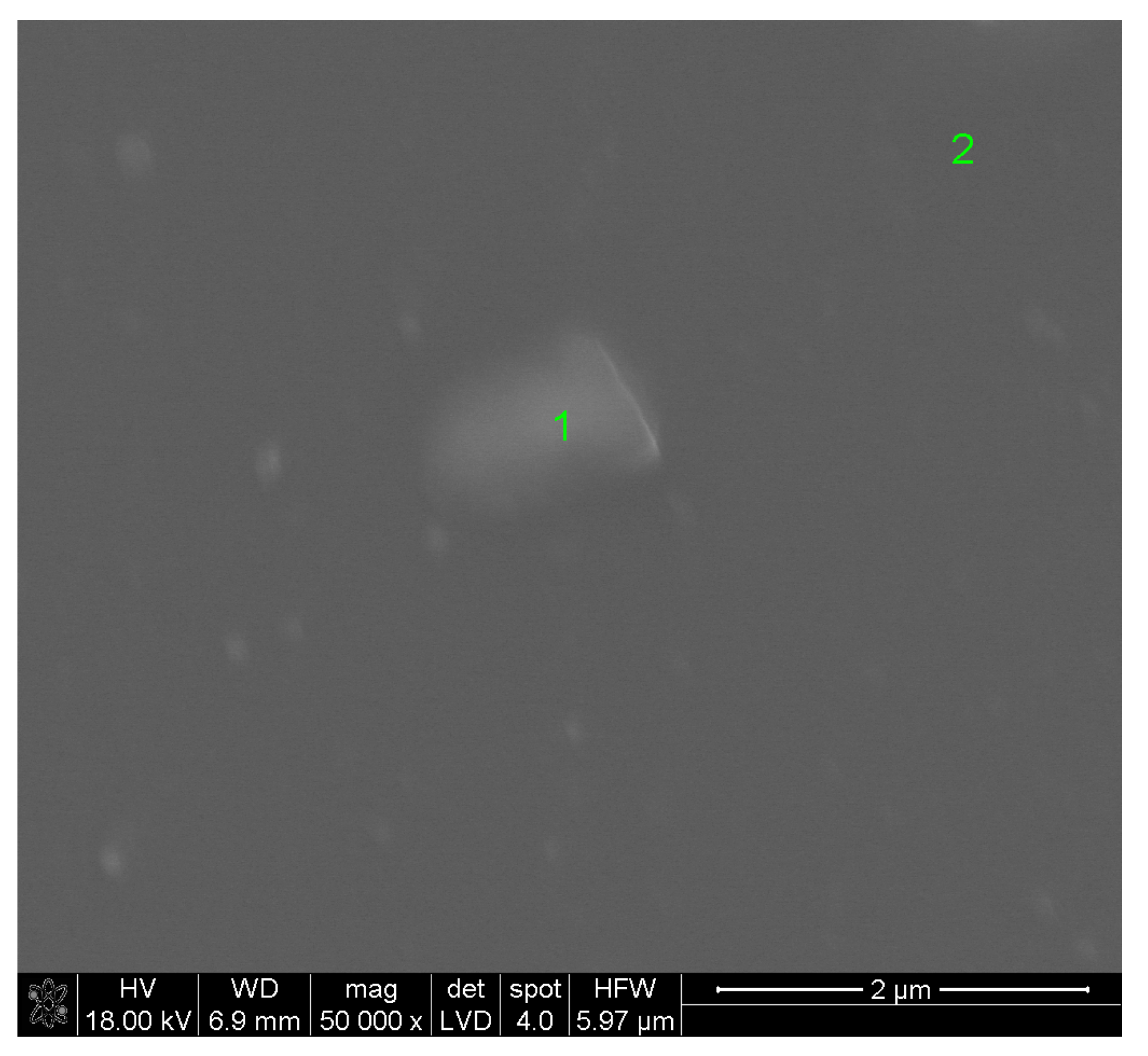
Figure 7 shows the surface of the ZrO
2-Sm
2O
3 layer synthesized at 550 °C with 14 mol.% Sm(tmhd)
3. The crystallite size is about 40 nm. Less crystallized darker areas (1) and more crystallized lighter areas (2) are visible. However, the number of crystalline nuclei in these areas is significantly lower than in the case of the samples presented in
Figure 1 and
Figure 6. The layer is not porous and smooth. From
Figure 7 it also follows that cracks on the layer surface after sample breaking are not visible, which additionally indicates that the layer is thinner and therefore its tensile strength is higher (which, as previously mentioned, follows Weibull’s theory and the C-G mechanism of crack propagation in brittle materials).
Table 3 and
Table 4 present quantitative results of EDS analyses performed at points 1 and 2, respectively (
Figure 7). The layer is lighter at point 1 than at point 2. Therefore, it should contain more Sm
2O
3.
Table 3.
Quantitative EDS analysis results obtained from point 1 on the surface of the sample presented in
Figure 7 (data only for Zr and Sm).
Table 3.
Quantitative EDS analysis results obtained from point 1 on the surface of the sample presented in
Figure 7 (data only for Zr and Sm).
| Element | Weight (%) | Atomic (%) |
|---|
| Zr | 6.96 | 1.61 |
| Sm | 1.75 | 0.25 |
Table 4.
Quantitative EDS analysis results obtained from point 2 on the surface of the sample presented in
Figure 7 (data only for Zr and Sm).
Table 4.
Quantitative EDS analysis results obtained from point 2 on the surface of the sample presented in
Figure 7 (data only for Zr and Sm).
| Element | Weight (%) | Atomic (%) |
|---|
| Zr | 7.05 | 1.65 |
| Sm | 1.09 | 0.15 |
From
Table 3 it follows that molar percentage of Sm
2O
3 at point 1 (
Figure 7) is equal to approximately 6.25%. If the theoretical efficiency of layer formation using these reactants equals 100% with 14 mol.% Sm(tmhd)
3, the Sm
2O
3 molar percentage in the layer would be 7%. Results contained in
Table 3 and
Table 4 have confirmed the above-mentioned assumptions that, at locations with greater crystalline phase content in the layer, there is less Sm
2O
3 than in areas with lower crystalline phase content.
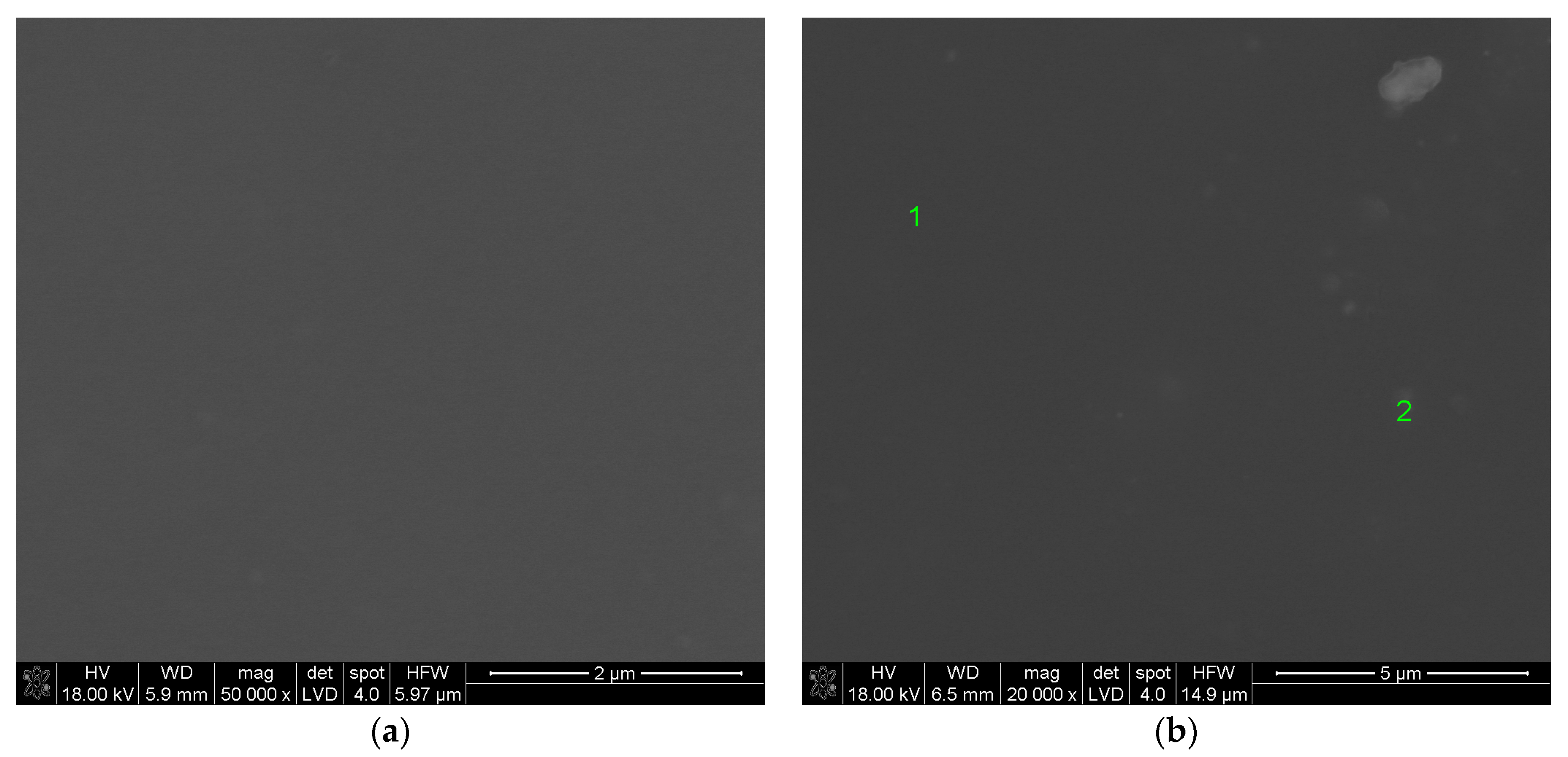
Figure 8 shows the surface of the layer synthesized at 500 °C (the molar percentage of Sm(tmhd)
3 was 14%). Other synthesis parameters are the same as in the case of the sample presented in
Figure 7. From
Figure 8 it follows that the layer is smooth and non-porous. Lighter crystalline areas and darker amorphous areas are also visible on this surface.
The crystallites with different sizes are smaller than those in
Figure 7. The size of the largest crystallites is about 30 nm. The layer is without cracks that form during sample breaking.
Table 5 contains the EDS analysis results obtained at point 1 (
Figure 8b). The area at point 1 is lighter compared to point 2 (
Figure 8), which can mean that there is lower amorphous phase content at point 1 (
Table 5) than at point 2 (
Table 6). The molar percentage of Sm
2O
3 is equal to 5.69%. From
Table 6 it follows that the molar content of Sm
2O
3 for point 2 amounts to 5.88%, so it is higher compared to that determined at point 1. However, the values are so similar that it is within the margin of error.
Table 5.
Quantitative EDS analysis results obtained from point 1 on the surface of the sample presented in
Figure 8b (data only for Zr and Sm).
Table 5.
Quantitative EDS analysis results obtained from point 1 on the surface of the sample presented in
Figure 8b (data only for Zr and Sm).
| Element | Weight (%) | Atomic (%) |
|---|
| Zr | 5.01 | 1.15 |
| Sm | 1.12 | 0.14 |
Table 6.
Quantitative EDS analysis results obtained from point 2 on the surface of the sample presented in
Figure 8b (data only for Zr and Sm).
Table 6.
Quantitative EDS analysis results obtained from point 2 on the surface of the sample presented in
Figure 8b (data only for Zr and Sm).
| Element | Weight (%) | Atomic (%) |
|---|
| Zr | 5.23 | 1.20 |
| Sm | 1.20 | 0.15 |
From the investigation results presented in
Figure 2 and
Figure 3 and
Table 1,
Table 2,
Table 3,
Table 4,
Table 5 and
Table 6 it can be concluded that there is a relationship between the chemical composition of synthesized layers and chemical composition of reactants in the gas phase. This indicates that, in the case of each sample, the synthesis process was controlled by the reactant diffusion to the substrate.
Additionally,
Figure 1,
Figure 2,
Figure 3,
Figure 4,
Figure 5,
Figure 6,
Figure 7 and
Figure 8 and the data included in
Table 1,
Table 2,
Table 3,
Table 4,
Table 5 and
Table 6 indicate that layers synthesized at low temperatures—i.e., 500 and 550 °C—have different thicknesses. Their chemical compositions in more or less crystallized areas are different when the molar contents of Sm(tmhd)
3 are different (14% and 22.75%). The weight of Zr(tmhd)
4 was similar for all samples, whereas the weight of Sm(tmhd)
3 changed. A significant difference in growth rate was also noted for these different molar contents.
It seems that analyzing the magnitude of the mass stream of reactants supplied to the substrate can provide a partial explanation for both cases. Detailed equations suitable for quantitative calculation of the magnitude of this stream for the
i-th reagent for different shapes of the substrate and reactor can be found in [
16,
19,
33].
In this work, two different molar contents of reactants were used. For this reason, differences in D and α values lead to different values of stream J
i to be transferred to the substrate and therefore layer growth can occur at different rates for different molar contents of Sm(tmhd)
3. It is believed that an increase in the molar content of Sm(tmhd)
3 in the reaction mixture probably triggered the mechanism of synergistic interaction of the reactants with each other, and possibly also the substrate for this process. In the case of the samples shown in
Figure 1 and
Figure 6, the difference in the growth rate of the layers synthesized at 500 and 550 °C is only about 22% in favor of those synthesized at 550 °C (in this case the molar percentage of Sm(tmhd)
3 was 22.75%). On the other hand, there is a large difference in the growth rate of the layers between the samples shown in
Figure 1 and
Figure 7 and the samples presented in
Figure 7 and
Figure 8 (obtained at temperatures of 500 and 550 °C with 14 mol.% Sm(tmhd)
3). In both cases, the substrates were cut from the same piece of quartz glass tube before the synthesis procedures and their further preparation for layer synthesis was similar.
It seems that a such an increase in the growth rate of ZrO
2-Sm
2O
3 layers synthesized at these two different molar contents of Sm(tmhd)
3 may be the result of catalytic action of increased Sm
2O
3 content in the ZrO
2-Sm
2O
3 layer synthesized when the molar percentage of Sm(tmhd)
3 was 22.75% in the growth process. Such catalytic action of Sm
2O
3 in ZrO
2-Sm
2O
3 layers deposited using the PVD method was observed by Shabalala et al. [
8]. High catalytic activity was indicated by layers when the molar percentage of Sm
2O
3 was approximately 2% (the crystallite size was 20–40 nm). When this value was lower or higher, this catalytic activity was lower.
