Latest Development on Pulsed Laser Deposited Thin Films for Advanced Luminescence Applications


Abstract
1. Introduction
2. Background and Theory
2.1. Laser Beam-Target Interaction
2.2. The Dynamics of Ablation of Materials and Plume Formation
2.3. The Evaporation of the Ablated Materials onto the Substrate
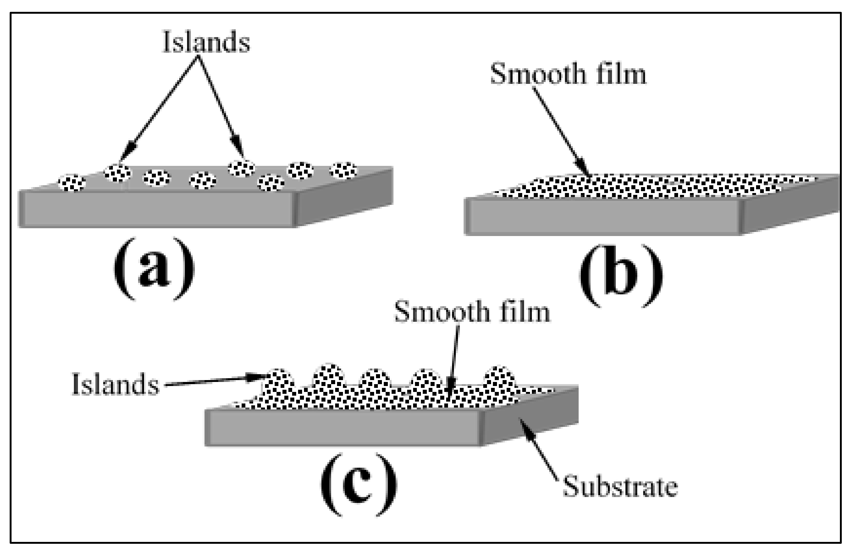
2.4. The Nucleation and Growth of a Thin Film on the Surface of the Substrate
2.5. Advantages and Disadvantages of PLD
3. Recently Modified PLD Arrangement
3.1. Scanning Multi-Component Pulsed Laser Deposition
3.2. Combined PLD and Magnetron Sputtering
3.3. Matrix Assisted Pulsed Laser Evaporation (MAPLE)
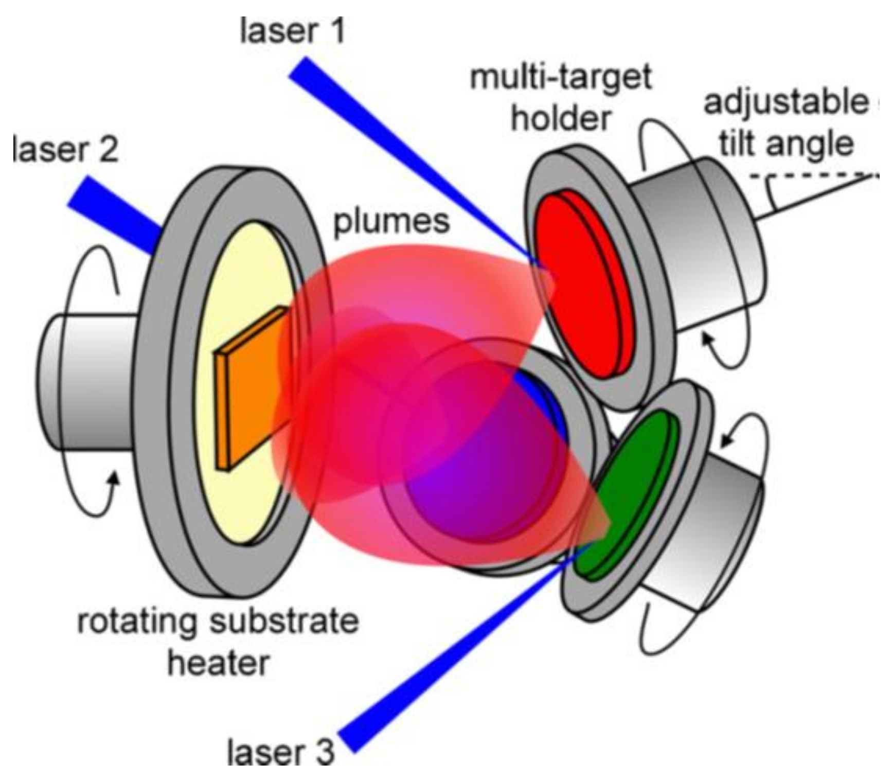
3.4. Multi-Beam PLD
3.5. Off-Axis PLD
4. Overview of Devices Fabricated Using PLD
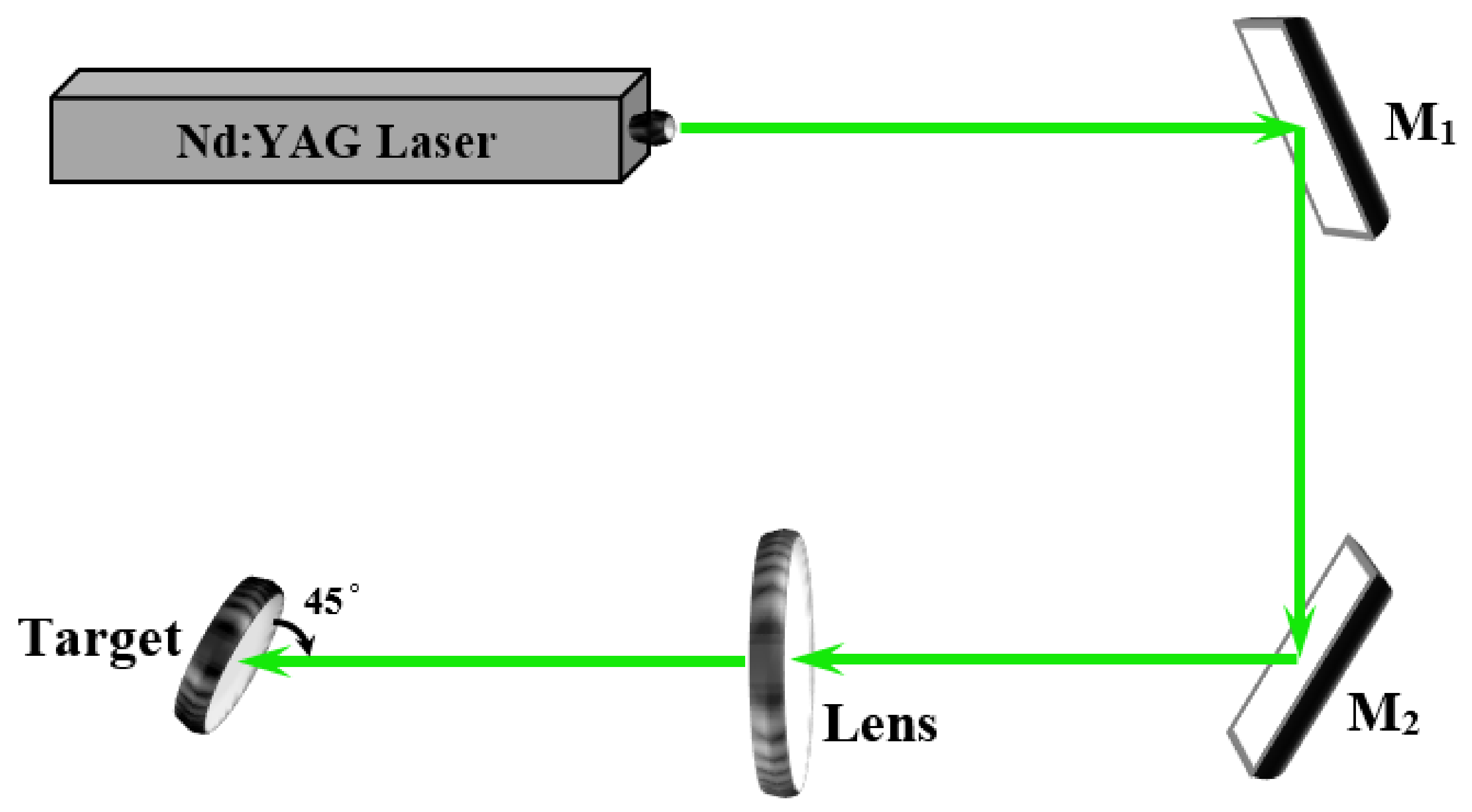
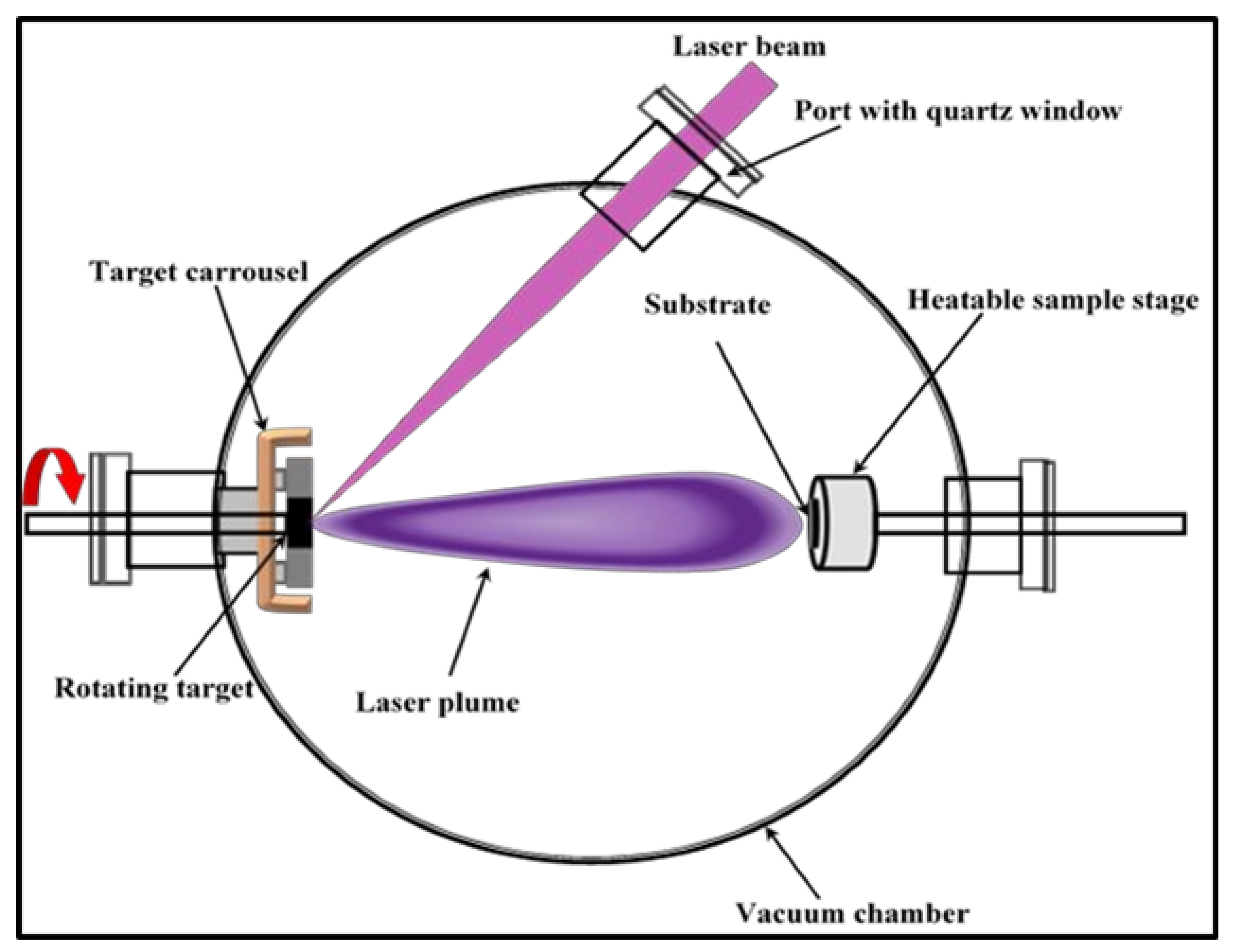
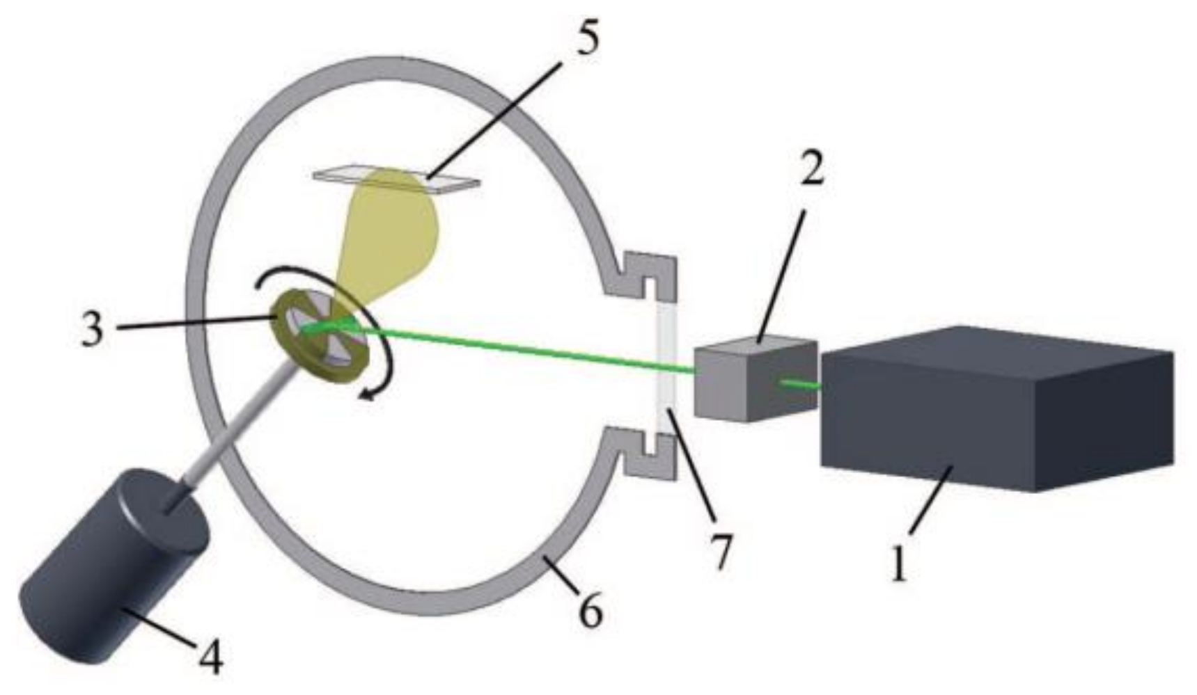
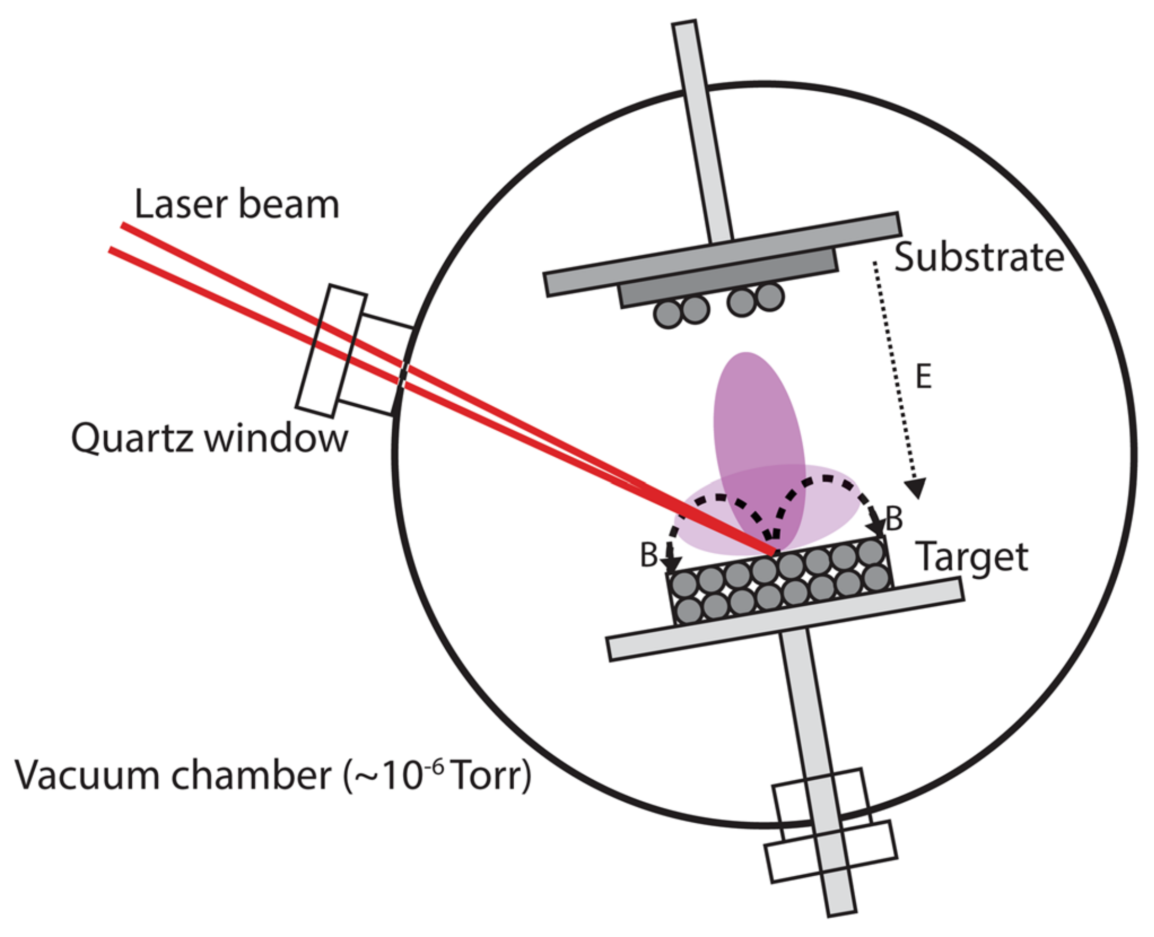
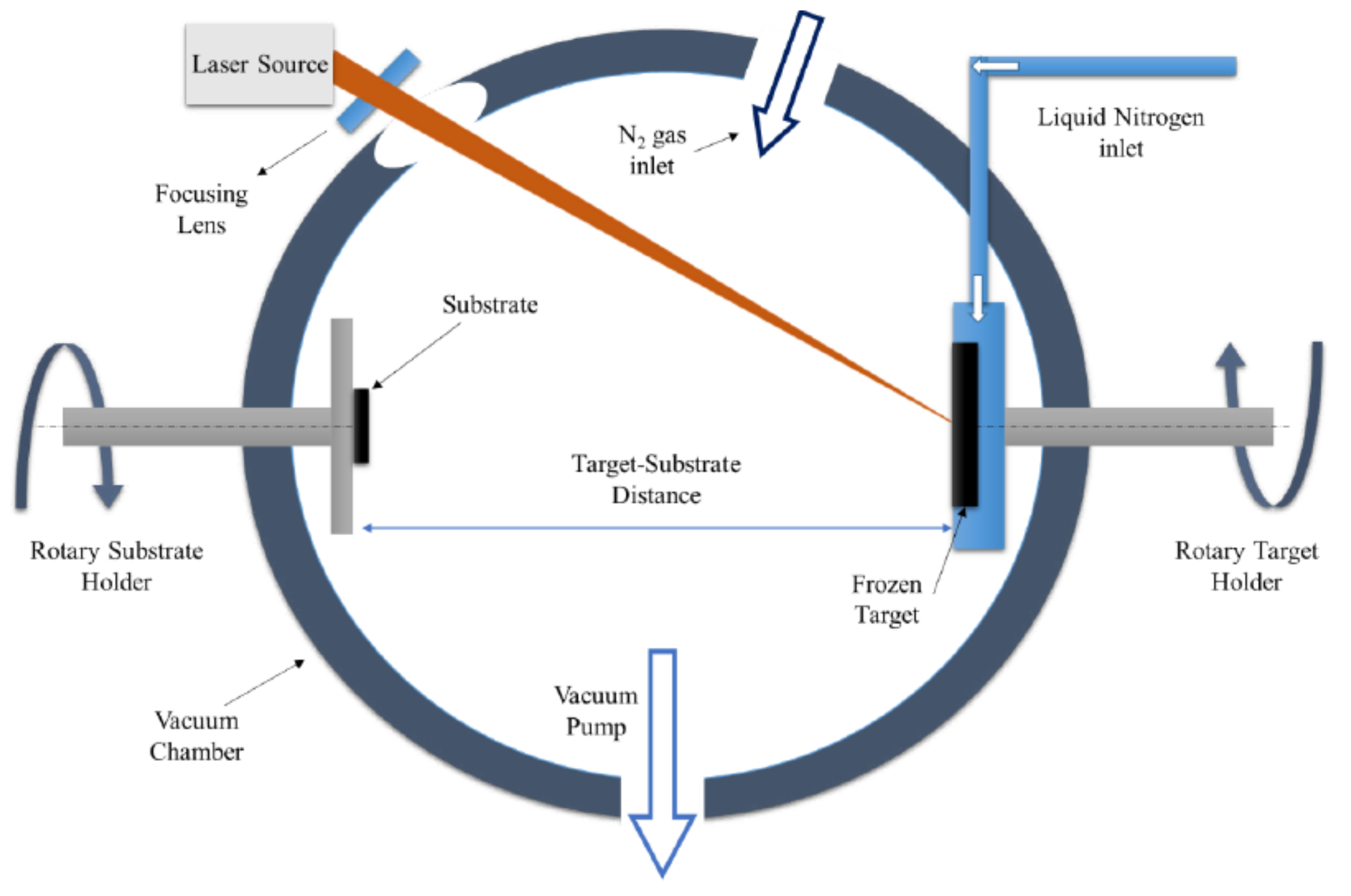
5. Experimental Procedure
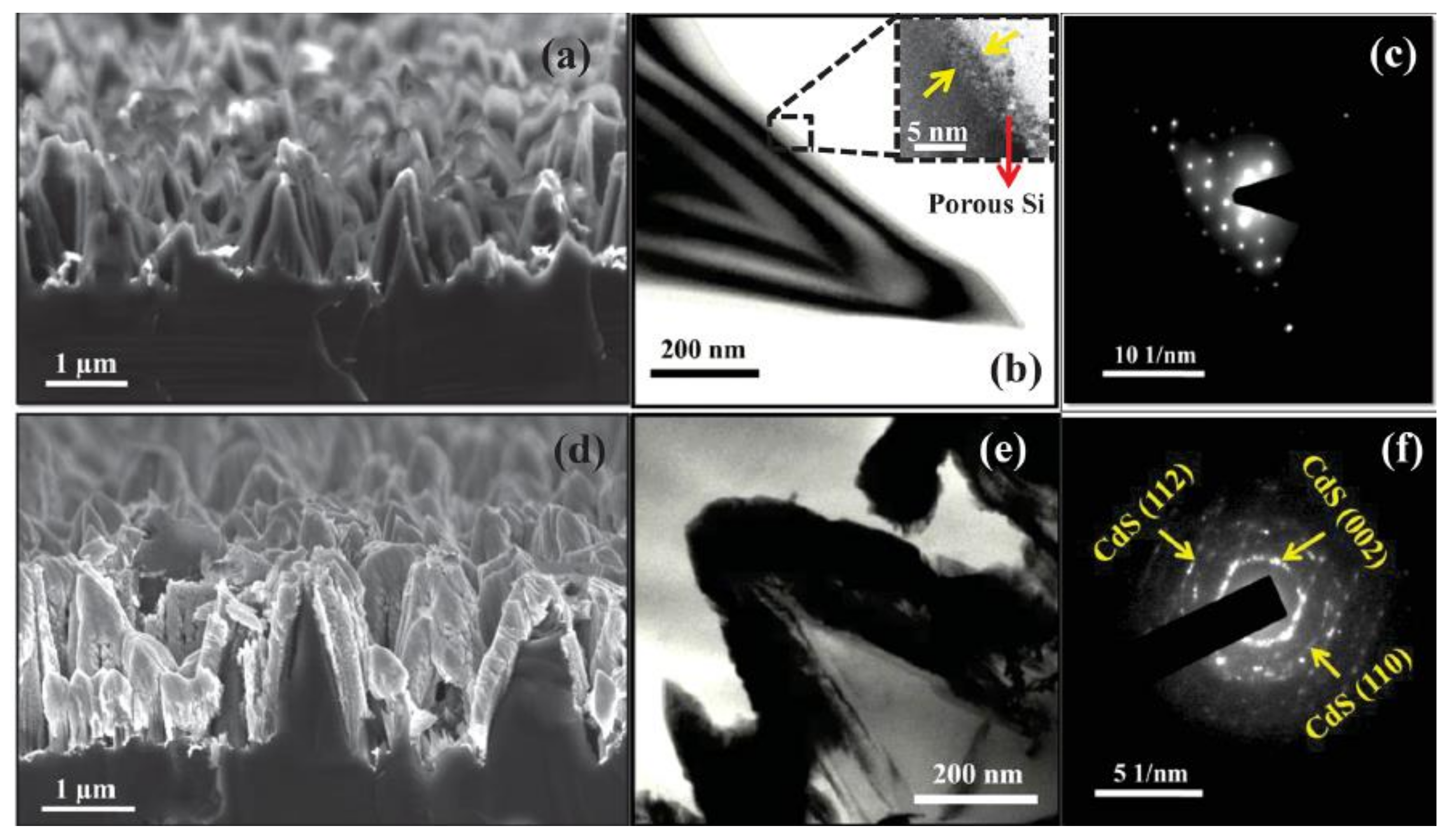
6. Structure, Morphologies and Luminescence of Thin Films Deposited Using PLD
7. Other Potential Applications of PLD
8. Conclusions and Challenges
Author Contributions
Funding
Acknowledgments
Conflicts of Interest
References
- Smith, H.M.; Turner, A.F. Vacuum deposited thin films using a ruby laser. Appl. Opt. 1965, 4, 147–148. [Google Scholar] [CrossRef]
- Dijkkamp, D.; Venkatesan, T.; Wu, X.D.; Shareen, S.A.; Jiswari, N.; Min-Lee, Y.H.; McLean, W.L.; Croft, M. Preparation of Y-Ba-Cu oxide superconductor thin films using pulsed laser evaporation from high Tc bulk material. Appl. Phys. Lett. 1987, 51, 619–621. [Google Scholar] [CrossRef]
- Venkayesan, T. (Ed.) Symposium I: Recent Advances in the Pulsed Laser Deposition of Thin Films and Nanostructures, MRS Singapore ICMAT Symposia Proceedings, Procedia Engineering; Elsevier: Amsterdam, The Netherlands, 2013. [Google Scholar]
- Norton, D.P. Pulsed laser deposition of complex materials: Progress towards applications. In Pulsed laser Deposition of Thin FILMS: Applications-Led Growth of Functional Materials; Eason, R., Ed.; John Wiley & Sons Inc.: Hoboken, NJ, USA, 2007; pp. 3–5. [Google Scholar]
- Krebs, H.; Weisheit, M.; Faupel, J.; Süske, E.; Scharf, T.; Fuhse, C.; Störmer, M.; Sturm, K.; Seibt, M.; Kijewski, H.; et al. Pulsed laser deposition (PLD)—A versatile thin film technique. In Advances in Solid State Physics; Kramer, B., Ed.; Springer: Berlin/Heidelberg, Germany, 2003; Volume 43, pp. 505–518. [Google Scholar] [CrossRef]
- Bleu, Y.; Bourquard, F.; Tite, T.; Loir, A.; Maddi, C.; Donnet, C.; Garrelie, F. Review of graphene growth from a solid carbon source by pulsed laser deposition (PLD). Front. Chem. 2018, 6, 572. [Google Scholar] [CrossRef] [PubMed]
- Coetsee, E.; Terblans, J.J.; Swart, H.C. Characteristic properties of Y2SiO5: Ce thin films grown with PLD. Phys. B Phys. Condens. Matter 2009, 404, 4431–4435. [Google Scholar] [CrossRef]
- Yousif, A.; Duvenhage, M.M.; Terblans, J.J.; Ntwaeaborwa, O.M.; Swart, H.C. Role of target and Ga particulates on the surface and optical properties of Y3(Al,Ga)5O12:Tb thin films prepared by PLD. Phys. B Phys. Condens. Matter 2018, 535, 319–322. [Google Scholar] [CrossRef]
- Gamaly, E.G.; Rode, A.V.; Davies, B.L. Ultrafast laser ablation and film deposition. In Pulsed Laser Deposition of Thin Films—Applications-Led Growth of Functional Materials; Eason, R., Ed.; John Wiley & Sons, Inc.: Hoboken, NJ, USA, 2007; pp. 99–129. [Google Scholar]
- Steen, W.M. Laser Material Processing; Springer: London, UK, 1991; pp. 81–89. [Google Scholar] [CrossRef]
- Bäuerle, D. Laser Processing and Chemistry, 3rd ed.; Springer: Berlin/Heidelberg, Germany, 2000; p. 221. [Google Scholar]
- Bäuerle, D. Laser Processing and Chemistry, 4th ed.; Springer: Berlin/Heidelberg, Germany, 2011; p. 20. [Google Scholar]
- Bäuerle, D. Laser Processing and Chemistry, 3rd ed.; Springer-Verlag: Berlin/Heidelberg, Germany, 2000; p. 226. [Google Scholar]
- Schou, J. Laser beam–solid Interactions: Fundamental aspects. In Materials Surface Processing by Directed Energy Techniques, 1st ed.; Pauleau, Y., Ed.; E-MRS: Great Britain, UK, 2006; pp. 35–66. [Google Scholar]
- Michail, C.M.; Toutountzis, A.; Valais, I.G.; Seferis, I.; Georgousis, M.; Fountos, G.; Kandarakis, I.S.; Panayiotakis, G.S. Luminescence efficiency of Gd2O2S: Eu powder phosphor as x-ray to light convertor. Sci. Technol. 2010, 2, 25–32. [Google Scholar]
- Soltan, S. Interaction of Superconductivity and Ferromagnetism in YBCO-LCMO Heterostructures; Cuvillier Verlag: Göttingen, Germany, 2005; p. 63. [Google Scholar]
- Nishinaga, T.; Scheel, H.J. Crystal growth aspects of high-Tc superconductors, In Advances in Superconductivity VIII; Hayakawa, H., Enomoto, Y., Eds.; Springer: Tokyo, Japan, 1996; pp. 33–38. [Google Scholar] [CrossRef]
- Le, P.H.; Luo, C.W. Thermoelectric and topological insulator bismuth chalcogenide thin films grown using pulsed laser deposition. In Applications of Laser Ablation—Thin Film Deposition, Nanomaterial Synthesis and Surface Modification; Yang, D., Ed.; InTech: Rijeka, Croatia, 2016; pp. 55–84. [Google Scholar]
- Richardson, J.J.; Lange, F.F. Low Temperature Continuous Circulation Reactor for the Aqueous Synthesis of ZnO Films, Nanostructures, and Bulk Single Crystals. US patent No: US 8926750 B2, 2015. [Google Scholar]
- Metev, S.; Meteva, K. Nucleation and growth of laser-plasma deposited thin films. Appl. Surf. Sci. 1989, 43, 402–408. [Google Scholar] [CrossRef]
- Schneider, C.W.; Lippert, T. Laser ablation and thin film deposition. In Laser Processing of Materials; Schaaf, P., Ed.; Springer Series in Materials Science; Springer: Berlin/Heidelberg, Germany, 2010; Volume 139, pp. 89–112. [Google Scholar] [CrossRef]
- Ogugua, S.N.; Nyenge, R.L.; Sechogela, P.T.; Swart, H.C.; Ntwaeaborwa, O.M. Influence of deposition atmosphere and substrate temperature on the structure, morphology, and photoluminescence of pulsed laser deposited La0.5Gd1.5SiO5:Dy3+. J. Vac. Sci. Technol. A 2016, 34, 021520-12. [Google Scholar] [CrossRef]
- Cheung, J.T. History and fundamentals of pulsed laser deposition. In Pulsed Laser Deposition of Thin Films, 1st ed.; Chrisey, D.B., Hubler, G.K., Eds.; Wiley Interscience: New York, NY, USA, 1994; pp. 1–19. [Google Scholar]
- Kumar, A.; Ganapathi, L.; Kanetkar, S.M.; Narayan, J. Single-chamber, in situ processing of superconducting YBa2Cu3O7−δ thin films on stainless steel with yttria-stabilized zirconia buffer layer. J. Appl. Phys. 1991, 69, 2410–2413. [Google Scholar] [CrossRef]
- Wu, K.H.; Chen, S.P.; Juang, J.Y.; Uen, T.M.; Gou, Y.S. Investigation of the evolution of YBa2Cu3O7−δ films deposited by scanning pulsed laser deposition on different substrates. Phys. C 1997, 289, 230–242. [Google Scholar] [CrossRef]
- Yap, S.S.; Tou, T.Y. Diamond-like carbon formation for various positions by pulsed laser deposition. Appl. Surf. Sci. 2005, 248, 340–343. [Google Scholar] [CrossRef]
- McGill, R.A.; Chrisey, D.B. Method of Producing a Film Coating by Matrix Assisted Pulsed Laser Deposition. US patent No: US 006025036A, 15 February 2000. [Google Scholar]
- Greer, J.A.; Howard, B.; Paradise, M.; Ivnitskiy, S.N.; Lations, D. Target Manipulation for Pulsed Laser Deposition. US patent No: US0067389A1, 2005. [Google Scholar]
- Fischer, D.; de la Fuente, G.F.; Jansen, M. A new pulsed laser deposition technique: Scanning multi-component pulsed laser deposition method. Rev. Sci. Instrum. 2012, 83, 043901–043908. [Google Scholar] [CrossRef] [PubMed]
- Benetti, D.; Nouar, R.; Nechache, R.; Pepin, H.; Sarkissian, A.; Rosei, F.; MacLeod, J.M. Combined magnetron sputtering and pulsed laser deposition of TiO2 and BFCO thin films. Sci. Rep. 2017, 7, 2503–2511. [Google Scholar] [CrossRef]
- Caricato, A.P.; Capone, S.; Epifani, M.; Lomascolo, M.; Luches, A.; Martino, M.; Romano, F.; Rella, R.; Siciliano, P.; Spadavecchia, J.; et al. Nanoparticle thin films deposited by MAPLE for sensor applications. In Fundamentals of Laser Assisted Micro- and Nanotechnologies; Veiko, V.P., Konov, V.I., Eds.; Springer: Cham, Switzerland; Heidelberg, Germany; New York, NY, USA, 2008; Volume 195. [Google Scholar]
- Piqué, A.; McGill, R.A.; Chrisey, D.B.; Leonhardt, D.; Mslna, T.E.; Spargo, B.J.; Callahan, J.H.; Vachet, R.W.; Chung, R.; Bucaro, M.A. Growth of organic thin films by the matrix assisted pulsed laser evaporation (MAPLE) technique. Thin Solid Films 1999, 355–356, 536–541. [Google Scholar] [CrossRef]
- Piqué, A. The Matrix-Assisted Pulsed Laser Evaporation (MAPLE) process: Origins and future directions. Appl. Phys. A 2011, 105, 517–528. [Google Scholar] [CrossRef]
- McGill, R.A.; Chrisey, R.B.; Pique, A.; Mlsna, T.E. Matrix-assisted pulsed-laser evaporation (MAPLE) of functionalized polymers: Applications with chemical sensors. In Laser Applications in Microelectronic and Optoelectronic Manufacturing III; Dubowski, J.J., Dyer, P.E., Eds.; Proc. SPIE: San Jose, CA, USA, 1999; Volume 3618, pp. 255–266. ISBN 0-8194-3088-9. [Google Scholar]
- Piqué, A.; Chrisey, D.B.; Spargo, B.J.; Bucaro, M.A.; Vachet, R.W.; Mlsna, T.; Leonhardt, D.; Mcgill, R.A.; Callahan, J.H.; Chung, R. Use of Matrix Assisted Pulsed Laser Evaporation (Maple) for the growth of organic thin films. MRS Proc. 1998, 526, 421–426. [Google Scholar] [CrossRef]
- Bloisi, F.; Cassinese, A.; Papa, R.; Vicari, L.; Califano, V. Matrix-Assisted Pulsed Laser Evaporation of polythiophene films. Thin Solid Films 2008, 516, 1594–1598. [Google Scholar] [CrossRef]
- Sima, F.; Davidson, P.; Pauthe, E.; Sima, L.E.; Gallet, O.; Mihailescu, I.N.; Anselme, K. Fibronectin layers by matrix-assisted pulsed laser evaporation from saline buffer-based cryogenic targets. Acta Biomater. 2011, 7, 3780–3788. [Google Scholar] [CrossRef] [PubMed]
- Caricato, A.P.; Luches, A. Applications of the matrix-assisted pulsed laser evaporation method for the deposition of organic, biological and nanoparticle thin films: A review. Appl. Phys. A 2011, 105, 565–582. [Google Scholar] [CrossRef]
- Yang, S.; Zhang, J. Matrix-Assisted Pulsed Laser Evaporation (MAPLE) technique for deposition of hybrid nanostructures. Front. Nanosci. Nanotechnol. 2017, 3, 1–9. [Google Scholar] [CrossRef]
- Kompitsas, M.; Giannoudakos, A.; Gyӧrgy, E.; Sauthier, G.; Figueras, A.; Mihailescu, I.N. Growth of metal-oxide semiconductor nanocomposite thin films by a dual-laser, dual target deposition system. Thin Solid Films 2007, 515, 8582–8585. [Google Scholar] [CrossRef]
- Gyӧrgy, E.; Sauthier, G.; Figueras, A.; Giannoudakos, A.; Kompitsas, M.; Mihailescu, I.N. Growth of Au–TiO2 nanocomposite thin films by a dual-laser, dual-target system. J. Appl. Phys. 2006, 100, 114302–114306. [Google Scholar] [CrossRef]
- Eason, R.W.; May-Smith, T.C.; Sloyan, K.A.; Gazia, R.; Darby, M.S.B.; Sposito, A.; Parsonage, T.L. Multi-beam pulsed laser deposition for advanced thin-film optical waveguides. J. Phys. D Appl. Phys. 2014, 47, 034007–034021. [Google Scholar] [CrossRef]
- Eason, R.W.; May-Smith, T.C.; Grivas, C.; Darby, M.S.B.; Shepherd, D.P.; Gazia, R. Current state-of-the-art of pulsed laser deposition of optical waveguide structures: Existing capabilities and future trends. Appl. Surf. Sci. 2009, 255, 5199–5205. [Google Scholar] [CrossRef]
- Veenas, C.L.; Nissamudeen, K.M.; Smitha, S.L.; Biju, V.; Gopchandran, K.G. Off-axis PLD: A novel technique for plasmonic engineering of silver nanoparticles. J. Optoelectron. Adv. M 2009, 11, 114–122. [Google Scholar]
- Hinton, M.J.; Yong, J.; Steers, S.; Lemberger, T.R. Comparison of 2-D quantum and thermal critical fluctuations of underdoped Bi2Sr2CaCu2O8+δ with ultrathin YBa2Cu3O7−δ. J. Supercond. Nov. Magn. 2013, 26, 2617–2620. [Google Scholar] [CrossRef]
- Siegert, M.; Zander, W.; Lisoni, J.; Schubert, J.; Buchal, C. Off-axis pulsed laser deposition system for epitaxial oxide growth on substrates up to 2 inches in diameter. Appl. Phys. A 1999, 69, S779–S781. [Google Scholar] [CrossRef]
- Elhmaidi, Z.O.; Abd-Lefdil, M.; El Khakani, M.A. Photoconversion Optimization of pulsed-laser-deposited p-CZTS/n-Si-nanowires heterojunction-based photovoltaic devices. Nanomaterials 2020, 10, 1393–13106. [Google Scholar] [CrossRef]
- Kadhim, A.; Harrison, P.; Meeth, J.; Al-Mebir, A.; Zeng, G.; Wu, J. Development of combinatorial pulsed laser deposition for expedited device optimization in CdTe/CdS thin-film solar cells. Int. J. Opt. 2016, 2016, 1–7. [Google Scholar] [CrossRef]
- Beloso, A.L.A.; Varela, M.D.B.; Rodríguez, A.F.; O’connor, G.; Trigo, E.P.; Álvarez, A.P.; García, D.N. Fabrication of a cell electrostimulator using pulse laser deposition and laser selective thin film removal. In Laser Ablation: From Fundamentals to Applications; Itina, T.E., Ed.; INTECH: Rijeka, Croatia, 2017; pp. 227–242. [Google Scholar] [CrossRef]
- Wang, B.; Zhang, Z.B.; Zhong, S.P.; Zheng, Z.Q.; Xu, P.; Zhang, H. Recent progress in high-performance photo-detectors enabled by the pulsed laser deposition technology. J. Mater. Chem. C 2020, 8, 4988–5014. [Google Scholar] [CrossRef]
- Sarkar, A.; Katiyar, A.K.; Mukherjee, S.; Singh, S.; Singh, S.K.; Das, A.K.; Ray, S.K. Geometry controlled white light emission and extraction in CdS/Black-Si conical heterojunctions. ACS Appl. Electron. Mater. 2019, 1, 25–33. [Google Scholar] [CrossRef]
- Kim, H.S.; Lugo, F.; Pearton, S.J.; Norton, D.P.; Wang, Y.L.; Ren, F. Phosphorus doped ZnO light emitting diodes fabricated via pulsed laser deposition. Appl. Phys. Lett. 2008, 92, 112108–112110. [Google Scholar] [CrossRef]
- Bayram, C.; Teherani, F.H.; Rogers, D.J.; Razeghi, M. Hybrid green LEDs based on n-ZnO/(InGaN/GaN) multi-quantum-wells/p-GaN. Proc. SPIE 2009, 7217, 72170P-7. [Google Scholar] [CrossRef]
- Cheng, X.; Xu, S.W.; Lu, Y.M.; Han, S.; Cao, P.J.; Jia, F.; Zeng, Y.X.; Liu, X.K.; Xu, W.Y.; Liu, W.J.; et al. Fabrication of tunable n-Zn1-xCdxO/p-GaN heterojunction light-emitting diodes. J. Alloys Compd. 2019, 776, 646–653. [Google Scholar] [CrossRef]
- Su, S.; Ling, C.; Azad, F.; Zeng, H.; Lu, Y.; Xing, S. Fabrication and modification of n-ZnO/p-GaN heterojunction light emitting diodes with white light emission characteristics. Nanosci. Nanotechnol. 2017, 9, 880–884. [Google Scholar] [CrossRef]
- Huang, Y.; Zhou, X.; Zhang, L.; Lin, G.; Xu, M.; Zhao, Y.; Jiao, M.; Zhang, D.; Pan, B.; Zhu, L.; et al. Tunable electroluminescence from an n-ZnO/p-GaN heterojunction with a CsPbBr3 interlayer grown by pulsed laser deposition. J. Mater. Chem. C 2020, 8, 12240–12246. [Google Scholar] [CrossRef]
- Zhang, L.; Li, Q.; Wang, F.; Qu, C.; Zhao, F. Room temperature electroluminescence from n-ZnO:Ga/i-ZnO/p-GaN:Mg heterojunction device grown by PLD. Electron. Mater. Lett. 2014, 10, 661–664. [Google Scholar] [CrossRef]
- Singh, J.; Srivastava, P.K.; Siwach, P.K.; Singh, H.K.; Tiwari, R.S.; Srivastava, O.N. PLD deposited ZnO films on different substrates and oxygen pressure: A study of surface morphology and optical properties. Sci. Adv. Mater. 2012, 4, 467–474. [Google Scholar] [CrossRef]
- Goyal, A.; Yadav, B.S.; Thakur, O.P.; Kapoor, A.K.; Muralidharan, R. Effect of annealing on β-Ga2O3 film grown by pulsed laser deposition technique. J. Alloys Compd. 2014, 583, 214–219. [Google Scholar] [CrossRef]
- Schilling, M.; Guillaume, A.; Scholtyssek, J.M.; Ludwig, F. Design of experiments for highly reproducible pulsed laser deposition of YBa2Cu3O7−δ. J. Phys. D. Appl. Phys. 2014, 47, 034008–034017. [Google Scholar] [CrossRef]
- Wakabayashi, R.; Oshima, T.; Hattori, M.; Sasaki, K.; Masui, T.; Kuramata, A.; Yamakoshi, S.; Yoshimatsu, K.; Ohtomo, A. Oxygen-radical-assisted pulsed-laser deposition of β-Ga2O3 and β-(AlxGa1−x)2O3 films. J. Cryst. Growth 2015, 424, 77–79. [Google Scholar] [CrossRef]
- Mandal, S.K.; Roy, R.K.; Pal, A.K. Effect of particle shape distribution on the surface plasmon resonance of Ag–SiO2 nanocomposite thin films. J. Phys. D Appl. Phys. 2003, 36, 261–265. [Google Scholar] [CrossRef]
- Ogugua, S.N.; Swart, H.C.; Ntwaeaborwa, O.M. Effects of deposition environment and temperature on photoluminescence, morphology, and crystal structure of pulsed laser deposited Ga2O3 thin films. J. Vac. Sci. Technol. A 2020, 38, 043407–043418. [Google Scholar] [CrossRef]
- Kumar, V.; Ntwaeaborwa, O.M.; Coetsee, E.; Swart, H.C. Role of deposition time on the properties of ZnO: Tb3+ thin films prepared by pulsed laser deposition. J. Colloid Interface Sci. 2016, 474, 129–136. [Google Scholar] [CrossRef]
- Shukla, G. ZnO/MgZnO p–n junction light-emitting diodes fabricated on sapphire substrates by pulsed laser deposition technique. J. Phys. D Appl. Phys. 2009, 42, 075105–075111. [Google Scholar] [CrossRef]
- Sulaiman, N.S.C.; Nee, C.H.; Yap, S.L.; Lee, Y.S.; Tou, T.Y.; Yap, S.S. The growth of nanostructured Cu2ZnSnS4 films by pulsed laser deposition. Appl. Surf. Sci. 2015, 354, 42–47. [Google Scholar] [CrossRef]
- Kim, H.; Horwitz, J.S.; Kafafi, Z.H.; Pique, A.; Kushto, G.P. Pulsed Laser Deposition of Transparent Conducting Thin Films on Flexible Substrates. US Patent No: US0068 18924B2, 11 November 2003. [Google Scholar]
- Allabergenov, B.; Chung, S.; Jeong, S.M.; Kim, S.; Choi, B. Enhanced blue photoluminescence realized by copper diffusion doping of ZnO thin films. Opt. Mater. Express 2013, 3, 1733–1741. [Google Scholar] [CrossRef]
- Hasabeldaim, E.; Ntwaeaborwa, O.M.; Kroon, R.E.; Coetsee, E.; Swart, H.C. Effect of substrate temperature and post annealing temperature on ZnO:Zn PLD thin film properties. Opt. Mater. 2017, 74, 139–149. [Google Scholar] [CrossRef]
- Hasabeldaim, E.; Ntwaeaborwa, O.M.; Kroon, R.E.; Motaung, D.E.; Coetsee, E.; Swart, H.C. Effect of PLD growth atmosphere on the physical properties of ZnO: Zn thin films. Opt. Mater. 2017, 74, 76–85. [Google Scholar] [CrossRef]
- Zheng, Z.Q.; Yao, J.D.; Yang, G.W. Growth of centimeter-scale high-quality In2Se3 films for transparent, flexible and high performance photodetectors. J. Mater. Chem. C 2016, 4, 8094–8103. [Google Scholar] [CrossRef]
- Dlamini, S.T.S.; Swart, H.C.; Terblans, J.J.; Ntwaeaborwa, O.M. The effect of different gas atmospheres on the structure, morphology and photoluminescence properties of pulsed laser deposited Y3(Al,Ga)5O12:Ce3+ nano thin films. Solid State Sci. 2013, 23, 65–71. [Google Scholar] [CrossRef]
- Splith, D.; Müller, S.; Schmidt, F.; von Wenckstern, H.; van Rensburg, J.J.; Meyer, W.E.; Grundmann, M. Determination of the mean and the homogeneous barrier height of Cu Schottky contacts on heteroepitaxial β-Ga2O3 thin films grown by pulsed laser deposition. Phys. Status Solidi A 2014, 211, 40–47. [Google Scholar] [CrossRef]
- Cai, Y.; Zhang, K.; Feng, Q.; Zuo, Y.; Hu, Z.; Feng, Z.; Zhou, H.; Lu, X.; Zhang, C.; Tang, W.; et al. Tin-assisted growth of ε-Ga2O3 film and the fabrication of photodetectors on sapphire substrate by PLD. Opt. Mater. Express 2018, 8, 3506–3517. [Google Scholar] [CrossRef]
- Nyenge, R.L.; Sechogela, P.T.; Swart, H.C.; Ntwaeaborwa, O.M. The influence of laser wavelength on the structure, morphology, and photoluminescence properties of pulsed laser deposited CaS: Eu2+ thin films. J. Mod. Opt. 2015, 62, 1102–1109. [Google Scholar] [CrossRef]
- Kato, K.; Dang, F.; Mimura, K.; Kinemuchi, Y.; Imai, H.; Wada, S.; Osada, M.; Haneda, H.; Kuwabara, M. Nano-sized cube-shaped single crystalline oxides and their potentials; composition, assembly and functions. Adv. Powder Technol. 2014, 25, 1401–1414. [Google Scholar] [CrossRef]
- Zhang, R.; Liu, X.; Shi, L.; Jin, X.; Dong, Y.; Li, K.; Zhao, X.; Li, Q.; Deng, Y. A Simple and Fast Method to Synthesize Cubic Iridium Nanoparticles with Clean Surface Free from Surfactants. Nanomaterials 2019, 9, 76. [Google Scholar] [CrossRef] [PubMed]
- Canham, L.T. Silicon quantum wire array fabrication by electrochemical and chemical dissolution of wafers. Appl. Phys. Lett. 1990, 57, 1046–1048. [Google Scholar] [CrossRef]
- Canham, L.T.; Leong, W.Y.; Beale, M.I.J.; Cox, T.I.; Taylor, L. Efficient visible electroluminescence from highly porous silicon under cathodic bias. Appl. Phys. Lett. 1992, 61, 2563–2565. [Google Scholar] [CrossRef]
- Katiyar, A.K.; Sinha, A.K.; Manna, S.; Ray, S.K. Fabrication of Si/ZnS radial nanowire heterojunction arrays for white light emitting devices on Si substrates. ACS Appl. Mater. Interfaces 2014, 6, 15007–15014. [Google Scholar] [CrossRef]
- Manna, S.; Das, S.; Mondal, S.P.; Singha, R.; Ray, S.K. High efficiency Si/CdS radial nanowire heterojunction photodetectors using etched Si nanowire templates. J. Phys. Chem. C 2012, 116, 7126–7133. [Google Scholar] [CrossRef]
- Sanz, M.; Walczak, M.; de Nalda, R.; Oujja, M.; Marco, J.F.; Rodriguez, J.; Izquierdo, J.G.; Bañares, L.; Castillejo, M. Femtosecond pulsed laser deposition of nanostructured TiO2 films. Appl. Surf. Sci. 2009, 255, 5206–5210. [Google Scholar] [CrossRef]
- Ullrich, B.; Sakai, H.; Segawa, Y. Optoelectronic properties of thin film CdS formed by ultraviolet and infrared pulsed-laser deposition. Thin Solid Films 2001, 385, 220–224. [Google Scholar] [CrossRef]
- Aguilar-Hernandez, J.; Contreras-Puente, G.; Morales-Acevedo, A.; Vigil-Galan, O.; Cruz-Gandarilla, F.; Vidal-Larramendi, J.; Escamilla-Esquivel, A.; Hernandez-Contreras, H.; Hesiquio-Garduno, M.; Arias-Carbajal, A.; et al. Photoluminescence and structural properties of cadmium sulphide thin films grown by different techniques. Semicond. Sci. Technol. 2003, 18, 111–114. [Google Scholar] [CrossRef]
- Abken, A.E.; Halliday, D.P.; Durose, K. Photoluminescence study of polycrystalline photovoltaic CdS thin film layers grown by close-spaced sublimation and chemical bath deposition. J. Appl. Phys. 2009, 105, 064515-9. [Google Scholar] [CrossRef]
- Kumar, S.; Singh, R. Nanofunctional gallium oxide (Ga2O3) nanowires/nanostructures and their applications in nanodevices. Phys. Status Solidi RRL 2013, 7, 781–792. [Google Scholar] [CrossRef]
- Harwig, T.; Kellendonk, F. Some observations on the photoluminescence of doped β-galliumsesquioxide. J. Solid State Chem. 1978, 24, 255–263. [Google Scholar] [CrossRef]
- Binet, L.; Gourier, D. Origin of the blue luminescence of β-Ga2O3. J. Phys. Chem. Solids 1998, 59, 1241–1249. [Google Scholar] [CrossRef]
- Tetsuyama, N.; Ishida, Y.; Higashihata, M.; Nakamura, D.; Okada, T. Fabrication of UV-LED using ZnO nanowires directly grown on p-GaN film by NAPLD. In Proceedings of the IEEE Conference on Lasers and Electro-Optics Pacific Rim (CLEO-PR), Kyoto, Japan, 30 June—4 July 2013; pp. 1–2. [Google Scholar] [CrossRef]
- Novoa-De León, I.C.; Johny, J.; Vázquez-Rodríguez, S.; García-Gómez, N.; Carranza-Bernal, S.; Mendivil, I.; Shaji, S.; Sepúlveda-Guzmán, S. Tuning the luminescence of nitrogen-doped graphene quantum dots synthesized by pulsed laser ablation in liquid and their use as a selective photoluminescence on–off–on probe for ascorbic acid detection. Carbon 2019, 150, 455–464. [Google Scholar] [CrossRef]
- Caballero-Briones, F.; Santana, G.; Flores, T.; Ponce, L. Photoluminescence response in carbon films deposited by pulsed laser deposition onto GaAs substrates at low vacuum. J. Nanotechnol. 2016, 2016, 1–6. [Google Scholar] [CrossRef]
- Yamada, Y.; Makino, T.; Suzuki, N.; Yoshida, T. Silicon nanocrystallite light emitting devices fabricated by full pulsed-laser-ablation process. Mat. Res. Soc. Symp. Proc. 2001, 638, F18-2. [Google Scholar] [CrossRef]
- Johnson, S.L.; Bowie, C.T.; Ivanov, B.; Park, H.K.; Haglund Jr, R.F. Fabrication of polymer LEDs by resonant infrared pulsed laser ablation. Proc. SPIE 2007, 6486, 64860G-9. [Google Scholar] [CrossRef]
- Hasabeldaim, E.; Ntwaeaborwa, O.M.; Kroon, R.E.; Swart, H.C. Surface analysis and cathodoluminescence degradation of undoped ZnO and ZnO:Zn phosphors. J. Vac. Sci. Technol. B 2016, 34, 041221-8. [Google Scholar] [CrossRef]
- Shukla, G.; Khare, A. Effect of annealing on structural and optical properties of pulsed laser deposited titanium dioxide thin films. Adv. Mater. Res. 2009, 67, 65–70. [Google Scholar] [CrossRef]
- Yousif, A.; Swart, H.C.; Ntwaeaborwa, O.M.; Coetsee, E. Conversion of Y3(Al,Ga)5O12:Tb3+ to Y2Si2O7:Tb3+ thin film by annealing at higher temperatures. Appl. Surf. Sci. 2013, 270, 331–339. [Google Scholar] [CrossRef]
- Yousif, A.; Swart, H.C.; Ntwaeaborwa, O.M. Improved luminescence properties of pulsed laser deposited Y3(Al,Ga)5O12:Tb thin films by post deposition annealing. J. Lumin. 2013, 143, 201–206. [Google Scholar] [CrossRef]
- Shen, W.P.; Kwok, H.S. Crystalline phases of II-VI compound semiconductors grown by pulsed laser deposition. Appl. Phys. Lett. 1994, 65, 2162–2164. [Google Scholar] [CrossRef][Green Version]
- Sohn, K.; Park, D.H.; Yoo, J.G.; Kim, J.S. Luminescence of pulsed laser deposited Y2SiO5:Tb3+ thin film phosphors on flat and corrugated quartz glass substrates. JPN J. Appl. Phys. 2005, 44, 1787–1791. [Google Scholar] [CrossRef]
- Nyenge, R.L.; Shaat, S.K.K.; Noto, L.L.; Mokoena, P.P.; Swart, H.C.; Ntwaeaborwa, O.M. TOF SIMS analysis, structure and photoluminescence properties of pulsed laser deposited CaS:Eu2+ thin films. J. Lumin. 2015, 167, 172–178. [Google Scholar] [CrossRef]
- Dolo, J.J.; Swart, H.C.; Coetsee, E.; Terblans, J.J.; Ntwaeaborwa, O.M.; Dejene, B.F. XPS analysis and luminescence properties of thin films deposited by the pulsed laser deposition technique. Hyperfine Interact. 2010, 197, 129–134. [Google Scholar] [CrossRef]
- Hirata, G.A.; Lopez, O.A.; Shea, L.E.; Yi, J.Y.; Cheeks, T.; McKittrick, J.; Siqueiros, J.; Avalos-Borja, M.; Esparza, A.; Falcony, C. Pulsed laser deposition of Y3Al5O12:Tb photoluminescent thin films. J. Vac. Sci. Technol. A 1996, 14, 1694–1696. [Google Scholar] [CrossRef]
- Ntwaeaborwa, O.M.; Nsimama, P.D.; Abiade, J.T.; Coetsee, E.; Swart, H.C. The effects of substrate temperature on the structure, morphology and photoluminescence properties of pulsed laser deposited SrAl2O4:Eu2+, Dy3+ thin films. Physica B 2009, 404, 4436–4439. [Google Scholar] [CrossRef]
- Botterman, J.; Joos, J.J.; Smet, P.F. Trapping and detrapping in SrAl2O4: Eu,Dy persistent phosphors: Influence of excitation wavelength and temperature. Phys. Rev. B 2014, 90, 085147-15. [Google Scholar] [CrossRef]
- Anoop, G.; Krishna, K.M.; Jayaraj, M.K. Photoluminescent studies in co-sputtered ZnGa2O4: Mn phosphor thin films. In Proceedings of the ASID; New Delhi, India: 8–12 October 2006; pp. 280–282.
- Yeung, K.M.; Tsang, W.S.; Mak, C.L.; Wong, K.H. Optical studies of ZnS:Mn films grown by pulsed laser deposition. J. Appl. Phys. 2002, 93, 3636–3640. [Google Scholar] [CrossRef]
- Geetha, M.; Singh, A.K.; Asokamani, R.; Gogia, A.K. Ti based biomaterials, the ultimate choice for orthopaedic implants—A review. Prog. Mater. Sci. 2009, 54, 397–425. [Google Scholar] [CrossRef]
- Jelínek, M.; Vaněk, P.; Tolde, Z.; Buixaderas, E.; Kocourek, T.; Studnička, V.; Drahokoupil, J.; Petzelt, J.; Remsa, J.; Tyunina, M. PLD prepared bioactive BaTiO3 films on TiNb implants. Mater. Sci. Eng. C 2017, 70, 334–339. [Google Scholar] [CrossRef]
- Yang, Y.; Wang, Z.; Li, J.; Viehland, D. Pulsed Laser Deposition of BaTiO3 Thin Films on Different Substrates. J. Nanomater. 2010, 2010, 756319. [Google Scholar] [CrossRef]
- Liu, Z. Laser Applied Coatings. Ref. Modul. Mater. Sci. Mater. Eng. Shreir’s Corros. 2010, 4, 2622–2635. [Google Scholar] [CrossRef]
- Murray, M.; Jose, G.; Richards, B.; Jha, A. Femtosecond pulsed laser deposition of silicon thin films. Nanoscale Res. Lett. 2013, 8, 272. [Google Scholar] [CrossRef]


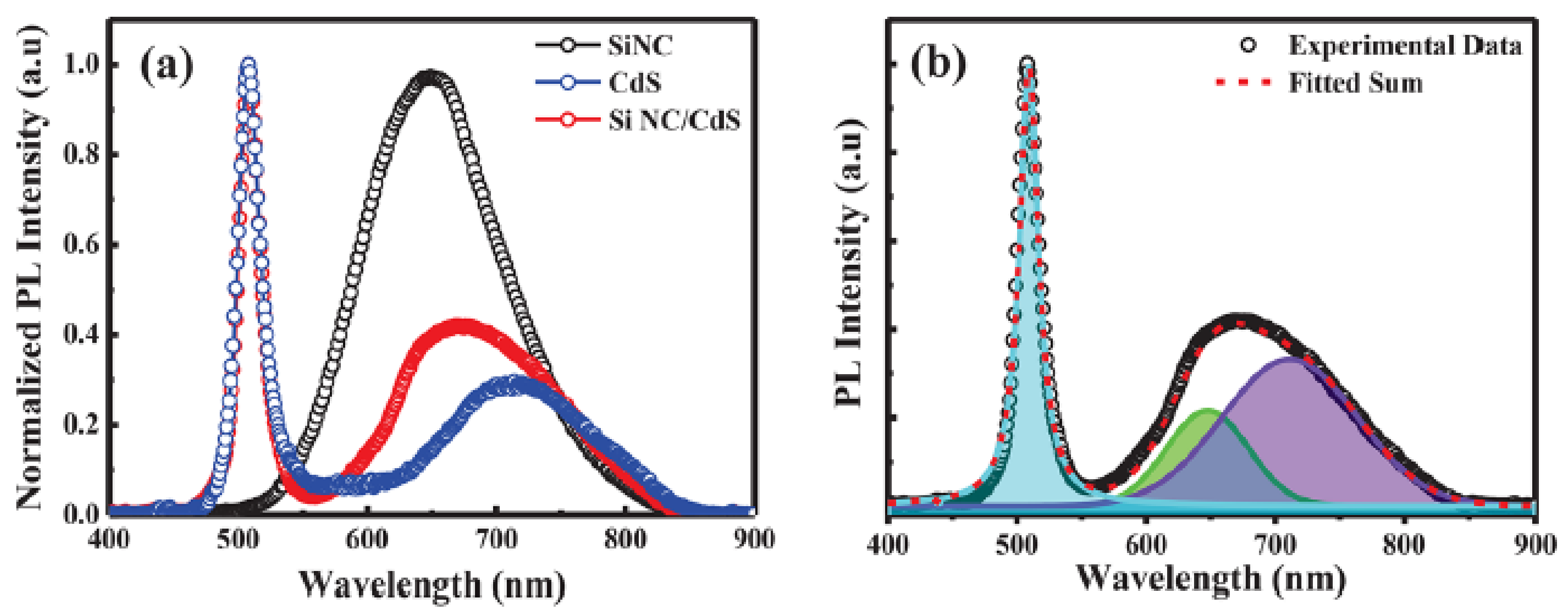
| Material | Substrate | Laser/Laser Parameters | Deposition Time (m) | Deposition Atmosphere | Substrate Temperature (°C) | Thickness (nm) | Ref |
|---|---|---|---|---|---|---|---|
| CdS/p ± bSi) | Si (100) | - | - | - | - | 50, 80 | [51] |
| ZnO/MgZnO | sapphire | Nd:YAG, λ = 532 RR = 10 LF = 1–2 PW = 8 | - | - | 800, 700, 650 | 8, 5, 100, 450 | [65] |
| Cu2ZnSnS4 | Si | Nd:YAG λ = 355 RR = 10 LF = 0.5−4 PW = 4.7 | 45 | - | 300 | 50 | [66] |
| ITO, AZO, | PET | KrF excimer λ = 248 RR = 10 LF = 1 PW = 30 | - | - | 25–125 | 100, 200 | [67] |
| ZnO:Cu | Si | KrF excimer λ = 248 RR = 2 LE = 400 | - | vacuum | - | 40, 300 | [68] |
| ZnO:Zn | Si (100) | Nd:YAG λ = 266 RR = 10 LE = 40 | 25 | vacuum, Ar, O2 | 300 | 80, 155, 285 | [69] |
| ZnO:Zn | Si (100) | Nd:YAG λ = 266 RR = 10 LF = 0.8 PW = 8 | 25 | O2 | 50, 200, 400 | 246, 414, 326 | [70] |
| In2Se3 | transparent polyimide | KrF excimer λ = 248 RR = 4 LE = 100 PW = 20 | 12.5 | O2 | 300 | 22.9 | [71] |
| Ga2O3 | Si (100) | Nd:YAG Λ = 266 RR = 50 LE = 40 | 15 | vacuum, Ar, O2 | 50–600 | 150 | [63] |
| ZnO:Tb3+ | Si (100) | Nd:YAG λ = 266 LE = 40 | 15-55 | O2 | 300 | 150–500 | [64] |
| Y3(Al,Ga)5O12:Ce3+ | Si (100) | Nd:YAG λ = 266 RR = 10 LF = 0.8 | - | Vacuum, Ar | 300 | 120, 270 | [72] |
| β-(AlxGa1-x)2O3 | β-Ga2O3 (010) | KrF excimer λ = 248 RR = 10 LF = 0.3 | - | O2 | 800 | 70, 79 | [61] |
| β-Ga2O3 | sapphire | KrF excimer λ = 248 LF = 2 | - | O2 | 650 | 250, 350, 500 | [73] |
| Ga2O3:Sn | sapphire | RR = 3 LF = 2 | - | O2 | 650 | 112, 445, 510, 570 | [74] |
| CaS:Eu2+ | Si (100) | Nd:YAG λ = 266 355, 532, RR = 10 LF = 5.09 LE = 40 | - | Ar | 400 | 150,162, 23 | [75] |
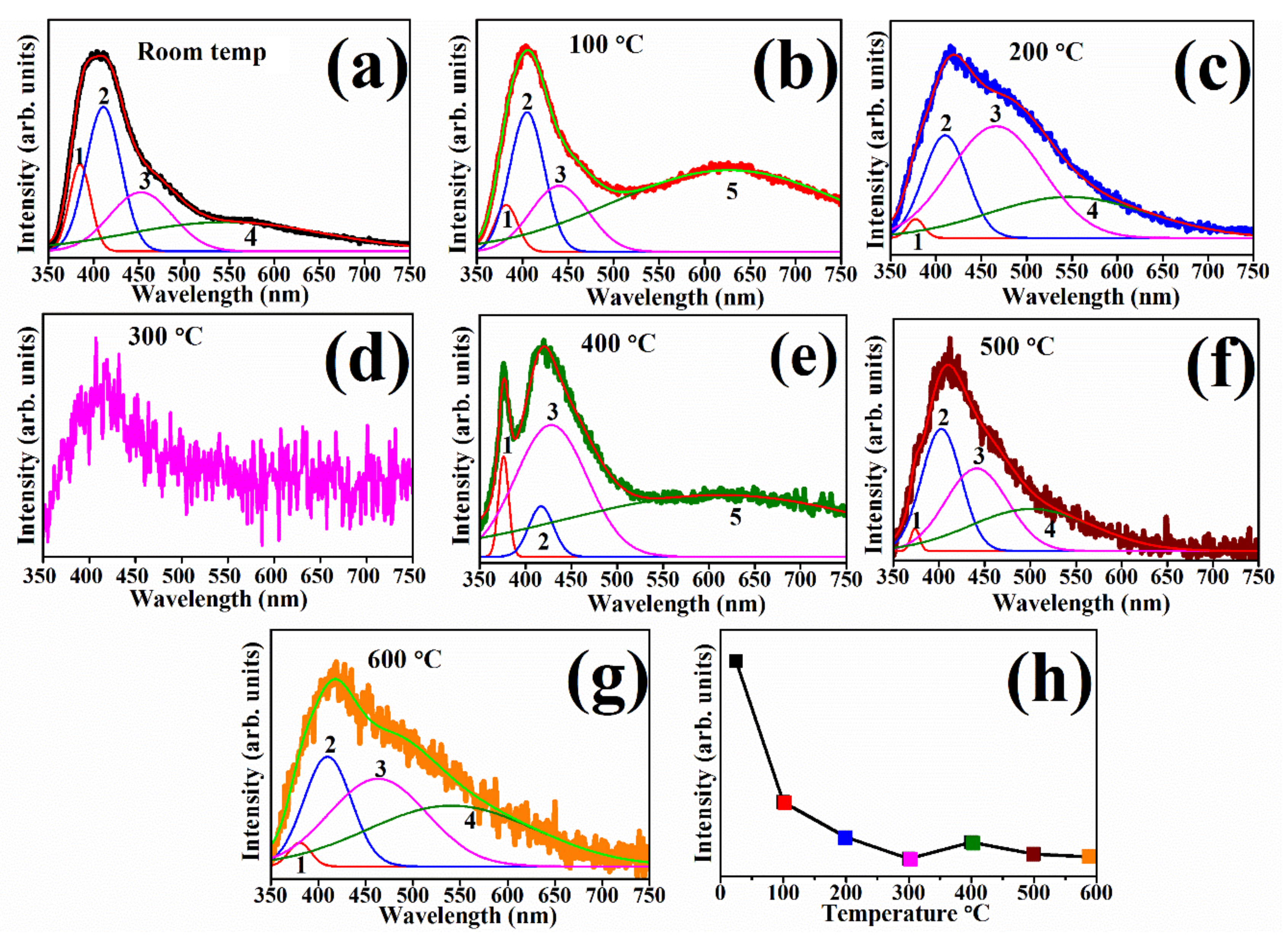
| Substrate Temperatures (°C) | Peak Positions (nm/eV) | ||||
|---|---|---|---|---|---|
| 1 | 2 | 3 | 4 | 5 | |
| Room Temperature | 385/3.22 | 410/3.02 | 454/2.73 | 575/2.16 | - |
| 100 | 383/3.24 | 404/3.07 | 440/2.82 | - | 630/1.97 |
| 200 | 376/3.30 | 410/3.02 | 466/2.66 | 555/2.23 | - |
| 300 | - | - | - | - | - |
| 400 | 376/3.30 | 417/2.97 | 429/2.89 | - | 630/1.97 |
| 500 | 376/3.30 | 404/3.07 | 440/2.82 | 510/2.43 | - |
| 600 | 378/3.28 | 410/3.02 | 464/2.67 | 544/2.28 | - |
| Material | Excitation Wavelength (nm) | Source(s) of Excitation | Emission Wavelength(s) (nm) | Source(s) of Emission | Ref. |
|---|---|---|---|---|---|
| ZnO:Zn | 325 | - | 514 | Oxygen vacancies | [94] |
| ZnO:Zn | 325 | - | 379, 405-450, 500-550, 600, 624, 658 | Exciton recombination, zinc vacancies, oxygen vacancies, oxygen interstitial, reduction of oxygen vacancies | [69] |
| ZnO:Zn | 325 | - | 378, 449, 550, 600 | Exciton recombination, zinc vacancy, oxygen vacancies, oxygen interstitials | [70] |
| TiO2 | - | - | 380-415 | Near-band-edge | [95] |
| Y3(Al,Ga)5O12:Tb3+, Y2Si2O7:Tb3+ | 227, 267 | 4f8 → 4f75d1 | 489, 544, 561, 625 | 5D4 → 7F6, 5D4 → 7F5, 5D4 → 7F4, 5D4 → 7F3 | [96] |
| Y3(Al,Ga)5O12:Tb | 229, 265 | 4f8 → 4f75d1 | 489, 544, 561, 625 | 5D4 → 7F6, 5D4 → 7F5, 5D4 → 7F4, 5D4 → 7F3 | [96,97] |
| La0.5Gd1.5SiO5:Dy3+ | 226 | Transition from oxygen 2p (O2p) valence band to the La(5d6s) and Gd(5d6s) conduction bands | 488, 578, 668, 756 | 4F9/2 → 6H15/2, 4F9/2 → 6H13/2, 4F9/2 → 6H11/12, 4F9/2 → 6H9/2 | [22] |
| ZnO:Tb3+ | 325 | - | 378, 415, 448, 517 | Band to band emission in ZnO, zinc vacancies, zinc interstitials, oxygen vacancies | [64] |
| Y3(Al,Ga)5O12:Ce3+ | 345, 435 | 2f7/2 → 5d | 502, 545 | 5d → 2f5/2, 5d → 2f7/2 | [72] |
| CdS | - | - | 499, 512 | impurity states, defects from host | [98] |
| Y2SiO5:Tb3+ | 254 | - | 489, 544, 561 | 5D4 → 7F6, 5D4 → 7F5, 5D4 → 7F4 | [96,99] |
| CaS:Eu2+ | 220, 470 | band-to-band, f → d | 618, 650 | 5D0 → 7F2, 4f6 [7f0 ]5d1 (t2g) → 4f7(8S7/2) | [100] |
| CaS:Eu2+ | 250, 320, 470 | band-to-band, 4f7[8S7/2] → 4f6[7FJ]5d1[eg], 4f7[8S7/2] → 4f6[7FJ]5d1[t2g] | 650 | 4f6 [7f0 ]5d1 (t2g) → 4f7(8S7/2) | [75] |
| Gd2O2S:Tb3+ | 275 | - | 490, 545, 588, 620 | 5D4 → 7F6, 5D4 → 7F5, 5D4 → 7F4, 5D4 → 7F3 | [101] |
| Y3Al5O12:Tb | 250 | - | 362, 398, 422, 470, 545, 570, 610 | 5D3 → 7F6, 5D3 → 7F5, 5D3 → 7F4, 5D4 → 7F6, 5D4 → 7F5, 5D4 → 7F4, 5D4 → 7F3 | [102] |
| SrAl2O4:Eu2+,Dy3+ | 325 | - | 525 | 5d–4f | [103,104] |
| ZnGa2O4:Mn | 290 | - | 508 | 4T1 → 6A1 | [105] |
| ZnS:Mn | 488 | - | 590 | 4T1(G) → 6A1(S) | [106] |
Publisher’s Note: MDPI stays neutral with regard to jurisdictional claims in published maps and institutional affiliations. |
© 2020 by the authors. Licensee MDPI, Basel, Switzerland. This article is an open access article distributed under the terms and conditions of the Creative Commons Attribution (CC BY) license (http://creativecommons.org/licenses/by/4.0/).
Share and Cite
Ogugua, S.N.; Ntwaeaborwa, O.M.; Swart, H.C. Latest Development on Pulsed Laser Deposited Thin Films for Advanced Luminescence Applications. Coatings 2020, 10, 1078. https://doi.org/10.3390/coatings10111078
Ogugua SN, Ntwaeaborwa OM, Swart HC. Latest Development on Pulsed Laser Deposited Thin Films for Advanced Luminescence Applications. Coatings. 2020; 10(11):1078. https://doi.org/10.3390/coatings10111078
Chicago/Turabian StyleOgugua, Simon N., Odireleng Martin Ntwaeaborwa, and Hendrik C. Swart. 2020. "Latest Development on Pulsed Laser Deposited Thin Films for Advanced Luminescence Applications" Coatings 10, no. 11: 1078. https://doi.org/10.3390/coatings10111078
APA StyleOgugua, S. N., Ntwaeaborwa, O. M., & Swart, H. C. (2020). Latest Development on Pulsed Laser Deposited Thin Films for Advanced Luminescence Applications. Coatings, 10(11), 1078. https://doi.org/10.3390/coatings10111078