Article

Multilayer Structure of Reduced Graphene Oxide and Copper Oxide as a Gas Sensor

1
Department of Electronics, AGH University of Science and Technology, Al. Mickiewicza 30, 30-059 Kraków, Poland
2
Faculty of Chemical and Process Engineering, Warsaw University of Technology, Waryńskiego 1, 00-645 Warsaw, Poland
*
Author to whom correspondence should be addressed.
Coatings 2020, 10(11), 1015; https://doi.org/10.3390/coatings10111015
Submission received: 26 August 2020 / Revised: 10 October 2020 / Accepted: 20 October 2020 / Published: 22 October 2020
(This article belongs to the Special Issue Metal Oxide Films and Their Applications)

Abstract

:
Reduced graphene oxide and copper oxide multilayer structures were fabricated in a planar configuration by deposition on both ceramic and Si/SiO2 substrates with interdigitated Au electrodes by the spray method. SEM (scanning electron microscopy), TEM (transmission electron microscopy), XRD (X-ray diffraction), and elemental analysis investigations indicated that graphene oxide (GO) was obtained in a form of interconnected flakes consisting of 6–7 graphene layers for GO with the total thickness of ca. 6 nm and 2–3 layers for rGO with the total thickness of 1 nm. The lateral size of one flake reached up to 10 micrometers. Copper oxide was obtained by the wet chemical method. The number of sequential layers of the sensing structure was optimized to obtain good sensitivity and acceptable response/recovery times in response to the oxidizing nitrogen dioxide atmosphere. Both semiconductor partners revealed p-type conductivity. Formation of isotype heterojunctions between both semiconductor partners was taken into account and their influence on electrical transport explained. Optimized sensor structures revealed relative sensitivities reaching several tens of percent and acceptable response and recovery times in NO2 concentration ranged from a few to 20 ppm. Possibility of manufacturing sensors working at room temperature was shown, but at the cost of prolonged response/recovery times.

1. Introduction

Traditionally, for sensing toxic gases, chemical sensors based on metal oxides are used. However, due the fact that these sensors work at elevated temperatures, which is connected with the consumption of an additional amount of power, adversely affecting long-term stability and integration with measurement electronics, there is still a need to have detectors working at possibly low temperatures and an increase in sensitivity below 1 ppm is also expected.
Recent investigations of graphene and its derivatives (i.e., epitaxial graphene (eG), doped graphene, graphene oxide (GO), or reduced graphene oxide (rGO)) indicate that these materials can be used as gas sensors working in the ppb region of gas concentration [1,2,3] and also at room temperature [2,4,5,6,7,8,9,10]. Intensive works are connected particularly with composites (hybrids) of the type GO/metal oxide [3,8,9,11,12,13,14,15,16,17,18], where CuO is used as one of these oxides [5,6,10]. Noble (Au, Ag, Pd, Pt) [2,7,19,20,21,22] and transition metal (Cu, Mn, Fe, Ni, and Co) [23,24,25] nanoparticles decorating GO due to their catalytic effect enhance the gas sensing performance of graphene. GO and its reduced state rGO are interesting from the point of view of sensor applications due to the presence of defect sites and many functional groups, interacting with the ambient atmosphere, which increases the sensitivity. On the other hand, defects in rGO are responsible for the increase in the adsorption energy of interacting gas and in effect, the increase in sensor recovery time. According to Zhang et al. [26], this adsorption energy increases from −0.40 eV for NO2 on pristine graphene to −3.04 eV on defective graphene. Reduction of GO to rGO can be performed in many ways (e.g., by using a reducing agent such as PSS (poly(sodium 4-styrenesulfonate) [27] or hydrazine [28]) and also by appropriate temperature annealing in air, which is the most popular method. In this work, reduction was performed by using both hydrazine and temperature annealing.
Multilayer technology of graphene/metal oxide adopted by the authors enables, on one hand, the exploitation of the very good detection properties of the metal oxide (sensitive essentially at elevated temperatures) and good sensitivity of rGO at low temperatures. On the other hand, the interaction of these two layers and formation of the isotype heterojunction increased the conductivity of the CuO layer that additionally enhanced the structure sensitivity observed even at room temperature. Interaction of the sensor with oxidizing NO2 gas is connected with the capture of electrons by adsorbed gas molecules, which leads to the decrease in resistance of both p-type materials. It is, however, necessary that the porosity of the multilayer will enable easy diffusion of gas molecules. Therefore in this work, the spray deposition method was adopted.
The sample preparation procedure and measurement setup were described in the first subsections and then the results of the films’ characterization performed with TEM, SEM, XRD, and elemental analysis experiments are given. An essential part of the work is, however, devoted to gas sensing measurements. The mechanism of gas sensing is described including the phenomena of gas chemisorption by the solid state surfaces and influence of heterojunctions formed at the particle interfaces on the transport properties. Sensitivity, response, and recovery times in different experimental conditions were characterized. Influence of the sensor substrate (alumina or crystalline silicon) on the sensor response was observed.

2. Materials and Methods

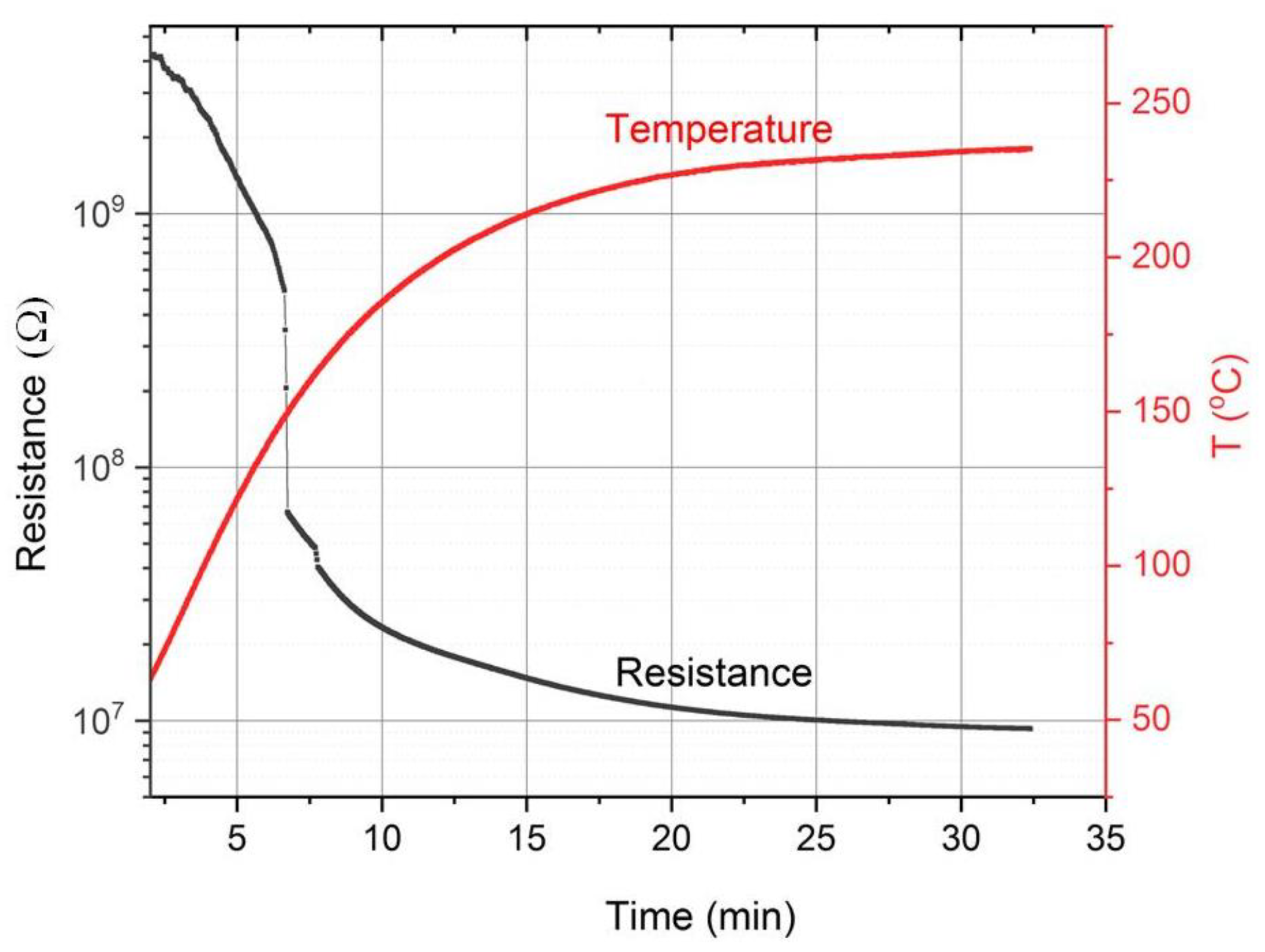
2.1. Sample Preparation

The samples in a form of a multilayer consisting of four layers (i.e., two layers of reduced graphene oxide rGO and two layers of CuO) were deposited by the spray method, Figure 1.
The deposition was performed in a sequence: rGO–CuO–rGO–CuO for four LbL structures, which is schematically illustrated in Figure 2 (CuO is always on top of the sample).
Graphene oxide was prepared using the modified Hummers method, as described previously in [29]. Graphite powder was treated with concentrated sulfuric acid, sodium nitrate, and potassium permanganate at a temperature around 10 °C. After 60 min, the temperature was increased up to 30 °C and was maintained under stirring for 2 h. After adding distilled water to the mixture, the temperature was increased up to 100 °C. A small amount of hydrogen peroxide was then added after 60 min. In order to purify the GO water suspension, the GO water slurry was filtrated and then rinsed with distilled water until the pH of the filtrate attained 6.0. In effect, the obtained single GO flakes reached up to six nanometers in thickness with 10 micrometers in a lateral size.
Technology of single CuO layers was similar to that described in [29]. In the case of the structure investigated in this work, the thickness and density of CuO layers varied from sample to sample due to the changing concentration of the CuO solution, from which the samples were prepared. In particular, the concentration of solution for the CuO sample labeled S1 was 0.0014%, 0.014%, for sample S2, and 0.14% for sample S3. Thickness of the GO layer was always the same. The samples were deposited on both ceramic substrates with interdigitated Au electrodes separated by 0.3 mm and on Si/SiO2 substrates with Au electrodes separated by ca. 5 μm (Figure 3).
The substrates with very low interelectrode separation were manufactured at the Institute of Electron Technology (ITE, Warsaw) using known lithography and etching processes in semiconductor technology. These substrates were used in particular for deposition and investigation of high-resistance GO samples.

2.2. Gas Sensing Measurement Setup

Assembled in the laboratory setup was used to measure the sensor signal (resistance) under variable conditions of humidity, gas concentration, and temperature (Figure 4). The measurement chamber of volume ca. 30 cm3 was heated from an Agilent 6643A power source. The chamber contained both investigated sensitive layers and a Pt100 temperature probe, which was connected to an Agilent 34970A digital multimeter. Humidity was measured just before the gas inlet with Sensirion SHT75 digital sensor (Sensirion AG, Zurich, Switzerland). As the investigated sensor resistance varied by several orders of magnitude, an electrometer Keithley 6517 (Keithley Instruments Inc., Cleveland, OH, USA), working in constant voltage mode was used. All devices were controlled from the Labview custom application by an Agilent Technologies 82357B USB/GPIB (Universal Serial Bus/General Purpose Interface Bus) interface card connected to a GPIB bus.
Investigated NO2 gas and air from the bottles (Air Products) were fed into mass flow valves/meters (model 1179 and 1459C, MKS Instruments, Deutschland, GmbH) to maintain a constant gas flow of 200 cm3/min. In order to assure stabilized gas humidity, a PID (proportional, integral, differential) algorithm-based humidity and mass flow controller (MFC) (MKS Instruments, Andover, MA, USA) was used together with a bubbler. In stabilized conditions, the humidity was maintained at the level of 0.1%. The required NO2 gas concentration was obtained by controlling the ratio of gas to air flow rates.

3. Results and Discussion

3.1. Characterization of Thin Films

TEM, SEM, and XRD images obtained for GO, rGO, and CuO samples are shown in Figure 5.
SEM and STEM pictures were recorded using a high resolution electron microscope HITACHI S-5500 (Hitachi Ltd, Tokyo, Japan). The XRD patterns were obtained by using an XRD diffractometer Bruker AXS DB Advance Cr (Kα 2.2910 Å) (Bruker AXS GmbH, Karlsruhe, Germany) with the use of a 0.015 mm vanadium filter. Comparing the images shown in Figure 5a,b, one can note in Figure 5b larger areas of higher transparency, which indicates a thinner sample of rGO due to the reduction process. Both graphene oxides were composed of flakes consisting of 6–7 graphene oxide sheets with the total thickness of ca. 6 nm for GO and 2–3 layers in a stacking nanostructure for rGO with the total thickness of ca. 1 nm. Lateral size of a single flake reached up to 10 micrometers, as was determined in detailed structural experiments. Within one flake, the medium can be considered as continuous.
Elemental compositions of graphene oxides determined by the elemental analysis method using a Thermo Scientific™ FLASH 2000 CHNS/O analyzer (Thermo Fisher Scientific, Waltham, MA, USA) are given in Table 1.
Reduction led to the increase in carbon atom concentration and the decrease in oxygen atoms, as expected.
The copper oxide covering graphene layer was composed essentially of nanowires, which is shown in Figure 5c,d. CuO nanowires have diameters less than 30 nm and lengths in the range of 500–1000 nm. The XRD pattern in Figure 5e corresponds to the monoclinic crystalline phase of CuO (a review of observed CuO microstructure morphologies and their gas sensing properties is given in [30]). Diffraction spectra in Figure 5f enabled the evaluation of the distance between graphene layers and the average height of stacking layers for both GO and rGO.

3.2. Gas Sensing Characteristics

Obtained samples were tested by measurements of electrical resistance in response to the ambient atmosphere. Initial resistance of the as-prepared structures was, however, in the GΩ range and the GO layers had to be reduced. Thermal reduction was carried out by annealing in increasing temperature conditions, as shown for GO in Figure 6.
All GO samples deposited onto ceramic substrates and thermally reduced, decreased its resistivity in a similar way, as shown in Figure 6. Thermally reduced GO deposited onto the Si/SiO2 substrate revealed the initial resistance of the order of tens MΩ and similarly to the dependence shown in Figure 6, started to decrease its value at ca. 180 °C. These observations (i.e., large decrease in resistance of rGO in comparison to GO) can be explained as a result of a decrease in the concentration of the oxygen functional groups attached to carbon [31,32,33]. The reduction process led to the decrease in the concentration of carbonyl C=O, epoxy C–O–C groups, and water molecules, which are the surface active defects influencing electrical transport. Removing of water additionally results in decreasing the distance between the graphene layers.
It should be mentioned that some parts of the samples were obtained in the reduced state by the interaction of GO with hydrazine hydrate. These rGO samples revealed as prepared resistance of the order tens kΩ and were not further reduced thermally.
Collected gas sensing characteristics for samples S1–S3 in interaction with oxidizing NO2 gas, the technology of which was shortly described in Section 2.1, are shown in Figure 7.
Change in technological conditions leading to the gradual increase in thickness of the CuO layers for samples from S1 to S3 also caused the change of response, as is shown in Figure 8a. The response, defined as (RaRg)/Ra, where Ra is the resistance in air and Rg is the resistance in a gas, increased with the increase in the thickness of CuO layers. With increasing sensor working temperature, the response mostly decreased (Figure 8).
For the comparison purposes, the sensitivity of a single rGO sample is also shown in Figure 8, indicating its lower response than these of rGO/CuO, particularly that of the S3 sample with the highest CuO layer thickness. Use of different substrates (i.e., alumina or Si/SiO2) indicates that the response to NO2 for samples deposited on alumina is higher than for those deposited on electronic grade silicon. This behavior can be explained as the influence of the substrate surface roughness, which is much higher for ceramic substrates and the sample surface exposed to interaction with the ambient gas is higher.
Response and recovery times for all investigated samples varied with temperature, which can be assessed from the analysis of Figure 7. The calculated recovery times were always higher in comparison to the response times shown in Figure 9 for sample S3 with the highest sensitivity. Response and recovery times decreased quickly, starting from a certain temperature. To explain this behavior, one should take into account the interaction process between the semiconductor surface and a gas molecule. Both adsorption and desorption processes depend on activation energies EA in relation to the thermal energy (i.e., EA/kBT), where kB is the Boltzmann constant. In this case, an increase in temperature caused a decrease in interaction time.
As can be deducted from the recent literature (see for example [3,4,5,20,21]), sensors based on rGO can also work at room temperature, which is beneficial from the point of view of applications, particularly in portable detectors.
The reproducibility of a temporal response at room temperature for multilayer sensors manufactured in the authors’ laboratory was checked, which is illustrated in Figure 10a. As can be seen, the sensor maintained its initial response amplitude without a clear decrease. With increasing gas concentration, the response to NO2 increased, which is shown in Figure 10b. This kind of nonlinear behavior indicating the process of sensor signal saturation was observed, for example, in [16,17].
Cross-sensitivity of the investigated sensors in response to the reducing atmosphere was checked by applying pulses of carbon monoxide in air. As shown in Figure 11, in the range of CO concentrations of the order of tens ppm and temperatures not exceeding 100 °C, the sensor was insensitive to CO. A small increase in the baseline resistance could only be noticed for long-lasting CO pulse duration of 60 min.
A similar effect of insensitivity to CO for composites SnO2/rGO used for NO2 sensing was observed by Neri et al. [11] and Zhang et al. [14]. In some cases, however, nanocomposites based on CuO/rGO may be very sensitive to CO, which can be ascribed to the specific sensor fabrication procedure.
Influence of the changing relative humidity on the response to the NO2 atmosphere was remarkable, as can be seen from Figure 12.
This effect could be expected, taking into account that the permeation of water molecules through GO flakes and dispersed CuO particles is easy. Taking this into account, all investigations of gas response were performed at a constant RH = 50%. In practical applications of the NO2 sensor based on presented structures and large variations of RH, some compensation of humidity influence should be envisaged. This can be done either by the application of special membranes acting as humidity traps or by using dedicated programming, utilizing information of the humidity level from an additional RH sensor. In a recent publication, it was shown that graphene oxide can even play the role of a molecular sieve in metal oxide-based hydrogen sensor [34].

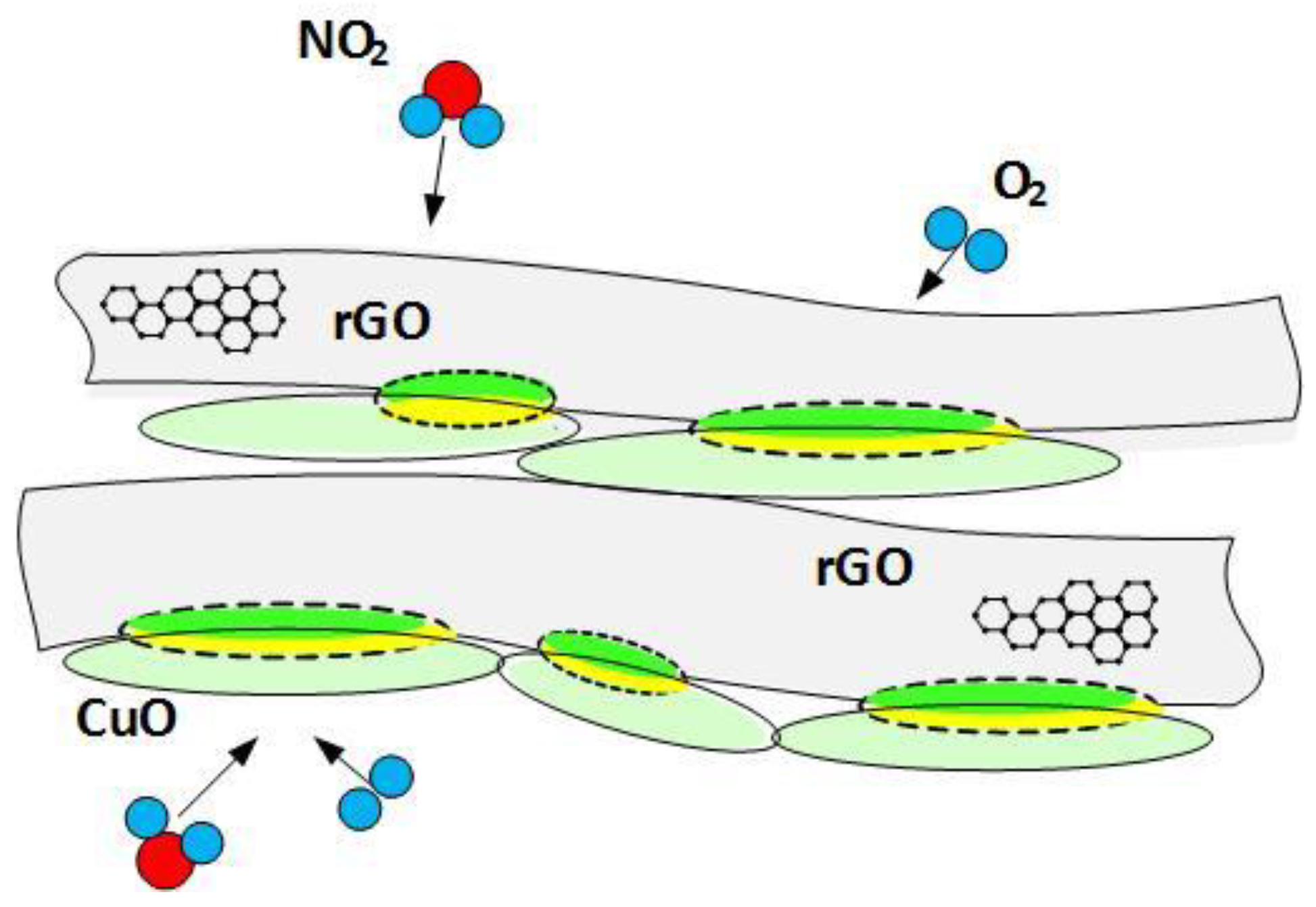
3.3. Sensing Mechanism

Single rGO layers decreased its resistance under the influence of oxidizing NO2 gas, which indicates that these samples are of the p-type. Capture of free electrons by NO2 caused the increase in the concentration of holes that manifest themselves in the decrease in rGO resistance. Single layers of CuO were also tested, but the samples deposited by the spray method revealed very high resistance. This resistance, similar to the rGO samples, decreased under the influence of NO2 atmosphere, indicating p-type conductivity. As shown above, for gas sensing experiments the authors used mostly the layer-by-layer rGO/CuO structures. Oxidizing properties of nitrogen dioxide resulted from its electronic structure. The unpaired electron is responsible for high electron affinity and in contact with the semiconductor surface NO2 attracts electrons.
In the analysis of the sensing mechanism, the temperature variations of the sensor response should be taken into account. Increase in the sensor working temperature activates the concentration of free carriers, which was observed as a decrease in the sensor base resistance in air. Moreover, variations in the sensors’ working temperature influence the chemisorption reactions of ambient gases (i.e., O2 and NO2) with both rGO and CuO surfaces (influence of temperature on the response and recovery times is discussed in the description of characteristics shown in Figure 8). The interaction of oxygen molecules with semiconductor nanostructures is widely accepted. In this case, several oxygen adsorbates can be formed. At temperatures below 100 °C, only one electron is absorbed and oxygen species Oads is formed. Above 100 °C, the species 2Oads, and above 300 °C, O2−ads can be formed, which is connected with the absorption of two electrons. Similarly, NO2 molecules exhibiting high electron affinity form surface adsorbates NO2. As suggested in [35], NO2 can also react with O2−ads, forming the complex NO3ads, which introduces the charge unbalance, and an additional electron is transferred from the semiconductor surface generating the hole. The multilayer structure of the investigated materials additionally enhanced the sensitivity. The pores in the layers and between layers act as additional channels for gas diffusion and provide more active sites for the adsorption processes.
Another factor than can influence electrical transport in the discussed multilayers is the possibility of the formation of heterojunctions at the rGO and CuO interface. This is schematically illustrated in Figure 13. Both junction partners are of p-type, but have different work functions that cause the charge transfer. Energetic structure of the a.m. heterojunction is illustrated in Figure 14.
The work function for rGO measured by Yang et al. [36], with the help of a Kelvin prober, equaled Φ1 = 5 ± 0.1 eV. Energy gap Eg1 = 1 eV was evaluated from [37] for oxygen content O/C in rGO equal ca. 10%. The work function for p-CuO nano-fibrils was determined from Fowler–Nordheim plots to be in the range of 4.1–4.3 eV [38], and the energy gap, equal Eg2 = 1.35, is given in [39].
As Φ2 is smaller than Φ1, electrons transfer from CuO to rGO and holes transfer in the opposite direction. This gives a depletion layer on the rGO side and an accumulation layer on the CuO side. In interaction with oxidizing NO2 gas electrons transfer from both rGO and CuO to the adsorbed NO2 molecules. In effect, the hole concentration in the CuO accumulation layer increases, resulting in the additional decrease in the multilayer resistance.

4. Conclusions

A reduced graphene oxide/copper oxide multilayer sensor was obtained by using the modified Hummers method for GO fabrication and wet chemical method for CuO production. The sensor structure was formed by sequential deposition of a selected number of layers on the substrate with interdigitated gold electrodes. Sensitivity and response/recovery times of the sensors vs. NO2 in air in the concentration range from a few to 20 ppm were investigated. Both semiconductor partners revealed p-type conductivity. Possibility of the formation of isotype heterojunctions between both semiconductor partners and their influence on sensitivity enhancement was taken into account. Appropriate selection of the multilayer composition enabled fabrication of nitrogen dioxide sensors with relative sensitivity reaching a few tens of percent and acceptable response and recovery times.

Author Contributions

Conceptualization, T.P., L.S., and A.R.; Methodology, T.P., L.S., and A.R.; Software, T.P.; Validation, T.P.; Formal analysis, A.R.; Investigation, W.M.; Resources, A.M. and W.M.; Data curation, T.P.; Writing—original draft preparation, T.P.; Writing—review and editing, A.R.; Visualization, D.M.; Supervision, T.P.; Project administration, A.R. and A.M.; Funding acquisition, A.R. All authors have read and agreed to the published version of the manuscript.

Funding

This research was funded by the National Science Centre Poland, grant No. UMO-2016/23/B/ST7/00894.

Acknowledgments

The paper was presented at the COE2020 Conference, Krakow, Poland.

Conflicts of Interest

The authors declare no conflict of interest.

References

  1. Iezhokin, I.; Offermans, P.; Brongersma, S.H.; Giesbers, A.J.M.; Flipse, C.F.J. High sensitive quasi freestanding epitaxial graphene gas sensor on 6H-SiC. Appl. Phys. Lett. 2013, 103, 053514-1–053514-5. [Google Scholar] [CrossRef] [Green Version]
  2. Ovsianytskyi, O.; Nam, Y.-S.; Tsymbalenko, O.; Lan, P.-T.; Moon, M.-W.; Lee, K.-B. Highly sensitive chemiresistive H2S gas sensor based on graphene decorated with Ag nanoparticles and charged impurities. Sens. Actuators B 2018, 257, 278–285. [Google Scholar] [CrossRef]
  3. Niavol, S.S.; Budde, M.; Papadogianni, A.; Heilmann, M.; Moghaddan, H.M.; Aldao, C.M.; Ligorio, G.; List-Kratochvil, J.W.; Lopes, J.M.J.; Barsan, N.; et al. Conduction mechanisms in epitaxial NiO/Graphene gas sensors. Sens. Actuators B 2020, 325, 128797. [Google Scholar] [CrossRef]
  4. Zhou, Y.; Jiang, Y.; Xie, T.; Tai, H.; Xie, G.A. Novel sensing mechanism for resistive gas sensors based on layered reduced graphene oxide thin films at room temperature. Sens. Actuators B 2013, 203, 135–142. [Google Scholar] [CrossRef]
  5. Sun, D.; Luo, Y.; Debliquy, M.; Zhang, C. Graphene-enhanced metal oxide gas sensors at room temperature: A review. Beilstein J. Nanotechnol. 2018, 9, 2832–2844. [Google Scholar] [CrossRef]
  6. Zhou, L.; Shen, F.; Tian, X.; Wang, D.; Zhang, T.; Chen, W. Stable Cu2O nanocrystals grown on functionalized graphene sheets and room temperature H2S gas sensing with ultrahigh sensitivity. Nanoscale 2013, 5, 1564–1569. [Google Scholar] [CrossRef] [PubMed]
  7. Ta, Q.T.H.; Namgung, G.; Noh, J.-S. Synthesis of Ag@rGO/g-C3N4 layered structures and their application to toxic gas sensors: Effect of Ag nanoparticles. Electron. Mater. Lett. 2019, 15, 750–759. [Google Scholar] [CrossRef]
  8. Galstyan, V.; Comini, E.; Kholmanov, I.; Ponzoni, A.; Sberveglieri, V.; Poli, N.; Faglia, G.; Sberveglieri, G. A composite structure based on reduced graphene oxide and metal oxide nanomaterials for chemical sensors. Beilstein J. Nanotechnol. 2016, 7, 1421–1427. [Google Scholar] [CrossRef] [Green Version]
  9. Zhang, D.; Liu, J.; Jiang, C.; Li, P.; Sun, Y. High-performance sulfur dioxide sensing properties of layer-by-layer self-assembled titania-modified graphene hybrid nanocomposite. Sens. Actuators B 2017, 245, 560–567. [Google Scholar] [CrossRef]
  10. Zhang, D.; Jiang, C.; Liu, J.; Cao, Y. Carbon monoxide gas sensing at room temperature using copper oxide-decorated graphene hybrid nanocomposite prepared by layer-by-layer self-assembly. Sens. Actuators B 2017, 247, 875–882. [Google Scholar] [CrossRef]
  11. Neri, G.; Leonardi, S.G.; Latino, M.; Donato, N.; Baek, S.; Conte, D.E.; Russo, P.A.; Pinna, N. Sensing behaviour of SnO2/reduced graphene oxide nanocomposites toward NO2. Sens. Actuators B 2013, 179, 61–68. [Google Scholar] [CrossRef]
  12. Chen, Z.-W.; Hong, Y.-Y.; Lin, Z.-D.; Liu, L.-M.; Zhang, X.-W. Enhanced formaldehyde gas sensing properties of ZnO nanosheets modified with graphene. Electron. Mater. Lett. 2017, 13, 270–276. [Google Scholar] [CrossRef]
  13. Liu, S.; Yu, B.; Zhang, H.; Fei, T.; Zhang, T. Enhancing NO2 gas sensing performance at room temperature based on reduced graphene oxide-ZnO nanoparticles hybrids. Sens. Actuators B 2014, 202, 272–278. [Google Scholar] [CrossRef]
  14. Zhang, H.; Feng, J.; Fei, T.; Liu, S.; Zhang, T. SnO2 nanoparticles-reduced graphene oxide nanocomposites for NO2 sensing at low operating temperature. Sens. Actuators B 2014, 190, 472–478. [Google Scholar] [CrossRef]
  15. Feng, Q.; Li, X.; Wang, J. Percolation effect of reduced graphene oxide (rGO) on ammonia sensing of rGO-SnO2 composite based sensor. Sens. Actuators B 2017, 243, 1115–1126. [Google Scholar] [CrossRef]
  16. Wang, W.H.; Han, W.; Pi, K.; McCreary, K.M.; Miao, F.; Bao, W.; Lau, C.N.; Kawakami, R.K. Growth of atomically smooth MgO films on graphene by molecular beam epitaxy. Appl. Phys. Lett. 2008, 93, 183107. [Google Scholar] [CrossRef]
  17. Punetha, D.; Kumar Pandey, S. Sensitivity enhancement of ammonia gas sensor based on hydrothermally synthesized rGO/WO3 nanocomposites. IEEE Sensors J. 2020, 20, 1738–1745. [Google Scholar] [CrossRef]
  18. Yin, F.; Li, Y.; Yue, W.; Gao, S.; Zhang, C.; Chen, Z. Sn3O4/rGO heterostructure as a material for formaldehyde gas sensor with a wide detecting range and low operating temperature. Sens. Actuators B 2020, 312, 127954. [Google Scholar] [CrossRef]
  19. Wu, J.; Ding, H.; Chen, J.; Wei, Y.; Wu, Z.; Wang, N.; Xie, X.; Shi, W.; Wang, X. Revealing the role of surface co-modification in boosting the gas sensing performance of graphene using experimental and theoretical evidences. Sens. Actuators B 2020, 316, 128162. [Google Scholar] [CrossRef]
  20. Shafiei, M.; Spizzirri, P.G.; Arsat, R.; Yu, J.; du Plessis, J.; Dubin, S.; Ianer, R.B.; Kalantar-Zadeh, K.; Wlodarski, W. Platinum/graphene nanosheet/SiC contacts and their application for hydrogen gas sensing. J. Phys. Chem. C1 2010, 114, 13796–13801. [Google Scholar] [CrossRef]
  21. Cho, B.; Yoon, J.; Hahm, M.G.; Kim, D.H.; Kim, A.R.; Khang, Y.H.; Park, S.-W.; Lee, Y.-J.; Park, S.-G.; Kwon, J.-D.; et al. Graphene-based gas sensor: Metal decoration effect and application to a flexible device. J. Mater. Chem. C 2014, 2, 5280–5285. [Google Scholar] [CrossRef]
  22. Kumar, R.; Varandani, D.; Mehta, B.R.; Singh, V.N.; Wen, Z.; Feng, X.; Muellen, K. Fast response and recovery of hydrogen sensing in Pd–Pt nanoparticle-graphene composite layers. Nanotechnology 2011, 22, 275719–275726. [Google Scholar] [CrossRef] [PubMed]
  23. Toh, R.J.; Poh, H.I.; Sofer, Z.; Pumera, M. Transition metal (Mn, Fe, Co, Ni) doped graphen hybrides for electrocatalysis. Chem. Asian. J. 2013, 8, 1295–1300. [Google Scholar] [CrossRef] [PubMed]
  24. Zhang, H.; Luo, X.; Song, H.; Lin, X.; Lu, X.; Tang, Y. DFT study of adsorption and dissociation behaviour of H2S on Fe-doped graphene. Appl. Surf. Sci. 2014, 317, 511–516. [Google Scholar] [CrossRef]
  25. Na, H.G.; Cho, H.J.; Kwon, Y.J.; Kang, S.Y.; Lee, C.; Jung, T.K.; Lee, H.-S.; Kim, H.W. Reduced graphene oxide functionalized with Cu nanoparticles: Fabrication, structure, and sensing properties. Thin Solid Films 2015, 588, 11–18. [Google Scholar] [CrossRef]
  26. Zhang, Y.-H.; Chen, Y.-B.; Zhou, K.-G.; Liu, C.-H.; Zeng, J.; Zhang, H.-L.; Peng, Y. Improving gas sensing properties of graphene by introducing dopants and defects: A first-principles study. Nanotechnology 2009, 20, 185504. [Google Scholar] [CrossRef] [Green Version]
  27. Stankovich, S.; Piner, R.D.; Chen, X.Q.; Wu, N.Q.; Nguyen, S.T.; Ruoff, R. Stable aqueous dispersions of graphitic nanoplatelets via the reduction of exfoliated graphite oxide in the presence of poly (sodium 4-styrenesulfonate). J. Mater. Chem. 2006, 16, 155–158. [Google Scholar] [CrossRef]
  28. Dreyer, D.R.; Park, S.; Bielawski, C.W.; Ruoff, R.S. The chemistry of graphene oxide. Chem. Soc. Rev. 2010, 39, 228–240. [Google Scholar] [CrossRef]
  29. Pisarkiewicz, T.; Maziarz, W.; Małolepszy, A.; Stobiński, L.; Michoń, D.; Rydosz, A. Gas sensing properties of reduced graphene oxide modified by copper oxide. In Proceedings of the 15th International Conference on Optical and Electronic Sensors COE 2018, Warsaw, Poland, 18–20 June 2018. [Google Scholar]
  30. Geng, W.; Ma, Z.; Zhao, Y.; Yang, J.; He, X.; Duan, L.; Li, F.; Hou, H.; Zhang, Q. Morphology-dependent gas sensing properties of CuO microstructures self-assembled from nanorod. Sens. Actuators B 2020, 325, 128775. [Google Scholar] [CrossRef]
  31. Stobiński, L.; Lesiak, B.; Malolepszy, A.; Mazurkiewicz, M.; Mierzwa, B.; Zemek, J.; Jiricek, P.; Bieloshapka, I. Graphene oxide and reduced graphene oxide studied by the XRD, TEM and electron spectroscopy methods. J. Electron. Spectr. Related Phenom. 2014, 195, 145–154. [Google Scholar] [CrossRef]
  32. Lipatov, A.; Verezhnikov, A.; Wilson, P.; Sysoev, V.; Kolmakov, A.; Sinitskii, A. Highly selective gas sensor arrays based on thermally reduced graphene oxide. Nanoscale 2013, 5, 5426–5434. [Google Scholar] [CrossRef] [PubMed] [Green Version]
  33. Lu, G.; Ocola, L.G.; Chen, J. Reduced graphene oxide for room temperature gas sensors. Nanotechnology 2009, 20, 445502. [Google Scholar] [CrossRef] [PubMed]
  34. Rasch, F.; Postica, V.; Schuett, F.; Mishra, Y.K.; Nia, A.S.; Lohe, M.R.; Feng, X.; Adelung, R.; Lupan, O. Highly selective and ultra-low power consumption metal oxide based hydrogen gas sensor employing graphene oxide as molecular sieve. Sens. Actuators B 2020, 320, 128363. [Google Scholar] [CrossRef]
  35. Yang, Y.; Tian, C.; Wang, J.; Sun, I.; Shi, K.; Zhou, W.; Fu, H. Facile synthesis of novel 3D nanoflower-like CuxO multilayer graphen composites for room temperature NOx gas sensor application. Nanoscale 2014, 6, 7369–7378. [Google Scholar] [CrossRef] [PubMed]
  36. Yang, H.; Li, Y.; Yu, D.; Li, L. Seed/catalyst free growth and self-powered photoresponse of vertically aligned ZnO nanorods on reduced graphene oxide nanosheets. Cryst. Growth Des. 2016, 16, 4831–4838. [Google Scholar] [CrossRef]
  37. Huang, H.; Li, Z.; She, J.; Wang, W. Oxygen density dependent band gap of reduced graphene oxide. J. Appl. Phys. 2012, 111, 054317. [Google Scholar] [CrossRef]
  38. Lin, H.H.; Wang, C.Y.; Shih, H.C.; Chen, J.M.; Hsieh, C.T. Characterizing well-oriented CuO nanofibrils synthesized through gas-solid reactions. J. Appl. Phys. 2004, 95, 5889–5894. [Google Scholar] [CrossRef]
  39. Park, W.J.; Choi, K.J.; Kim, M.H.; Koo, B.H.; Lee, J.-L.; Baik, J.M. Self-assembled and highly selective sensors based on air-bridge-structured nanowire junction arrays. ACS Appl. Mater. Interfaces 2013, 5, 6802–6807. [Google Scholar] [CrossRef]
Figure 1. (a) Schematic of the preparation process of CuO and (b) deposition of GO/CuO multilayer by spraying.
Coatings 10 01015 g001
Figure 2. Schematic of the sample geometry illustrating the view of the upper two layers of the multilayer structure.
Coatings 10 01015 g002
Figure 3. (a) Ceramic substrate (BVT Technologies) with masking layer (blue) enabling deposition of two samples in the same process and (b) Si/SiO2 substrate with interdigitated gold electrodes manufactured with the help of lithography technology.
Coatings 10 01015 g003
Figure 4. Illustration of a measurement setup used for determination of the gas sensing characteristics of the investigated structures.
Coatings 10 01015 g004
Figure 5. TEM images of GO (a) and rGO; (b) flakes; (c), (d) SEM images of CuO nanoparticles with different magnifications; (e) X-ray diffraction pattern of CuO; and (f) X-ray diffraction pattern for GO and rGO.
Coatings 10 01015 g005
Figure 6. An example of transformation of GO into rGO by annealing in atmospheric air.
Coatings 10 01015 g006
Figure 7. Variation of resistance of a multilayer sensor structures 4LbL with measurement temperature during interaction with NO2 pulses of a concentration 4 ppm in air. Thickness of the CuO layers increased from S1 to S3.
Coatings 10 01015 g007
Figure 8. (a) Variation of response to 4 ppm NO2 vs. temperature for multilayer rGO/CuO 4LbL structures (S1–S3) with changing CuO thickness and for a single rGO sample. (b) Comparison of responses to NO2 for rGO samples deposited on both alumina and Si/SiO2 substrates.
Coatings 10 01015 g008
Figure 9. Variation of response and recovery times vs. temperature for sample S3.
Coatings 10 01015 g009
Figure 10. (a) Variation of resistance a multilayer rGO/CuO structure 6LbL vs. time at room temperature in interaction with 20 ppm NO2 pules and (b) change of this response with increasing NO2 gas concentration.
Coatings 10 01015 g010
Figure 11. Change of S2 sample resistance in response to CO pulse of concentration 20 ppm at 50% RH and at sensor temperatures of (a) 48 °C and (b) 100 °C.
Coatings 10 01015 g011
Figure 12. Response of the S2 sample at 100 °C to 10 ppm and 20 ppm NO2 with the changing relative humidity of water vapor in air.
Coatings 10 01015 g012
Figure 13. Multilayer rGO/CuO. Possibility of heterojunction formation is shown.
Coatings 10 01015 g013
Figure 14. Isotype p-rGO/p-CuO heterojunction with a hole accumulation layer on the CuO side and a hole depletion layer on the rGO side. Φ1 and Φ2 are work functions of the junction partners, Vbi is the built-in potential.
Coatings 10 01015 g014
Table 1. Elemental composition of GO/rGO.
SampleC (wt %)O (wt %)N (wt %)H (wt %)Others (wt %)
GO45.5147.810.232.454.0
rGO85.559.953.201.050.25
Publisher’s Note: MDPI stays neutral with regard to jurisdictional claims in published maps and institutional affiliations.

