Photoluminescence of Layered Semiconductor Materials for Emission-Color Conversion of Blue Micro Light-Emitting Diode (µLED)


1
Department of Electrical and Computer Engineering, Faculty of Engineering, Shinshu University, 4-17-1 Wakasato, Nagano 380-8553, Japan
2
Research Initiative for Supra-Materials, Shinshu University, 4-17-1 Wakasato, Nagano 380-8533, Japan
*
Author to whom correspondence should be addressed.
Coatings 2020, 10(10), 985; https://doi.org/10.3390/coatings10100985
Submission received: 16 September 2020
/
Revised: 9 October 2020
/
Accepted: 13 October 2020
/
Published: 15 October 2020
Abstract
:A micro light-emitting diode (μLED) is a key device for the future of advanced information. Owing to expand its application widely, the concept of the emission-color conversion using layered semiconductors as a color converter is proposed. In addition, it is demonstrated that layered semiconductors were transferred directly onto μLED chips, and the emission-color conversion is realized. The layered GaS1−xSex alloy, whose energy bandgap can be controlled by tuning the S and Se compositions, was selected as a color converter. The photoluminescence (PL) measurements using a blue LED as an excitation source revealed that GaS0.65Se0.35 and GaSe can show green and red luminescence with center energies of 2.34 and 1.94 eV, respectively. The emission color of gallium nitride (GaN)-based blue μLEDs covered with GaS0.65Se0.35 and GaSe thin films were clearly converted to green and red, respectively. Furthermore, the emission color could be controlled by changing the film thickness. Thus, these results suggest the possibility of emission-color conversion of blue μLED chips utilizing layered materials.
1. Introduction
Micro light-emitting diodes (μLEDs) based on gallium nitride (GaN) material systems have received much attention in novel optoelectronic technologies such as next-generation display and wireless communication for the internet of things as well as in interdisciplinary fusion such as biomedical applications [1,2,3]. In particular, a head-mounted display for virtual reality, augmented reality and these kinds desire full-color light-emitting devices have been expected as specific application examples. This is because of their properties including high brightness, high response speed, long device lifetime, low power operation, and the realization of microfabrication. Therefore, μLEDs are expected to be used as a key device underpinning the future of advanced information society. To achieve the above-mentioned applications, the emission color of GaN-based μLEDs is converted from blue or near-ultraviolet light to visible light, such as green, yellow and red by several methods, as shown in Figure 1a. In any case, the emission-color conversion of GaN-based μLEDs achieves utilizing principles of fluorescence or photoluminescence (PL). Directly coated phosphors or colloidal quantum dots (QDs) can be realized the emission-color conversion from blue to various visible colors [4,5,6,7,8,9]. These color converters should be at least several micrometres (μm) thick because of the realization of high light absorption and high-efficiency luminescence. In addition, II-VI based quantum wells (QW) on glass substrates are also investigated as the color converter [10,11]. Although QW structures with reflectors can be designed below 5 μm thick, the carrier substrate is approximately 200 μm. Ideally, the thickness of the color converter should be thinner and ultimately negligible for any further miniaturization and integration expanding to the application for other products.
On the other hand, layered materials are also expected for optoelectronic device applications on a micro- and nano-scale. The thickness can be controlled by exfoliating from the bulk form, and the thin film can be arranged directly onto other materials through van der Waals forces by the transfer method. In addition, their characteristics of luminescence exhibit high potential of them being used as photonic materials [12,13,14,15]. Therefore, a combination of GaN-based μLEDs and layered materials is one of the candidate methods for realizing full-color μLEDs miniaturized in all dimensions, as shown in Figure 1b. However, this approach of color conversion has not yet been demonstrated. Note that the luminescence characteristics of layered materials are generally achieved via the microscopic PL measurement using a solid-state laser as an excitation source, and the luminescence is detected using an optical detector through an optical microscope and a spectrometer. In particular, the high visibility of luminescence after converting GaN-based μLEDs is important in this approach for any application. Thus, it is an important issue to demonstrate the emission-color conversion of GaN-based μLEDs using layered materials. Transition metal dichalcogenides (TMDCs) such as molybdenum and tungsten dichalcogenides (MoX2 and WX2, X: S or Se) have been extensively studied for luminescence characteristics in layered materials, and its nanosheet has excellent light absorption characteristics compared to other optoelectronic materials. However, the light absorption efficiency is about 20% at most, therefore, it is difficult to realize PL by exciting at the output level of the LED. In addition, there are few investigated nanosheet materials with green luminescence. In this study, gallium sulfur selenium (GaS1−xSex) alloys showing green and red luminescence were utilized for the first demonstration of emission-color conversion combining with GaN-based μLEDs and layered materials. We report the color conversion from blue to green and red lights for GaN-based μLEDs using semiconducting GaS1−xSex alloys as a color converter of layered material. First, the compositions of GaS1−xSex alloy were designed to obtain green and red luminescence. Next, PL measurement of GaS1−xSex films was performed using a shell-type blue LED to determine whether color conversion could be achieved at the output level of an LED light. Then, GaS1−xSex films were exfoliated and transferred onto the device chips, and the emission-color conversions of GaN-based μLEDs from blue to cyan, green and red were realized.
2. Materials and Method
Vapor-grown bulk GaSSe and GaSe alloys were prepared for color converters of green and red luminescence, respectively. For the GaSSe alloy, the S and Se compositions were estimated by using the lattice constant determined through X-ray diffraction (XRD) and Vegard’s law (Figure S1). The PL was obtained using a microscopic PL system based on HORIBA LabRAM HR Evolution. A commercially available shell-typed LED with blue emission at a center wavelength of 470 nm was used as an excitation source for PL measurements. The blue light of the LED was incident on the samples from the back side through the microscope glass. The PL signal was detected by a charge-coupled device through an optical microscope and a spectrometer with a grating of 1800 lines/mm.
Flip-chip-bonded blue μLED chips (130 × 240 μm2) were purchased from the Epistar Corporation. Typical characteristics of μLED operation include a turn-on voltage of 2.5 V and external quantum efficiency of more than 25% at a current density of 300 A/cm2 (Figure S2). GaSSe and GaSe thin films with the thickness below 100 μm were obtained by mechanical exfoliation onto μLED chips. The devices were operated with a probe station equipped with tungsten needles connected to a source measure unit (2450, Keithley, Solonm, OH, USA) at room temperature for electroluminescence (EL) measurements. To observe color conversion from blue to green and red, the emission light was monitored using a fiber optic spectrometer (Ocean Optics, FLAME-S, Amersham, UK).
3. Results and Discussion
3.1. Compositions of Layered GaS1−xSex Alloy for Green and Red Luminescenes
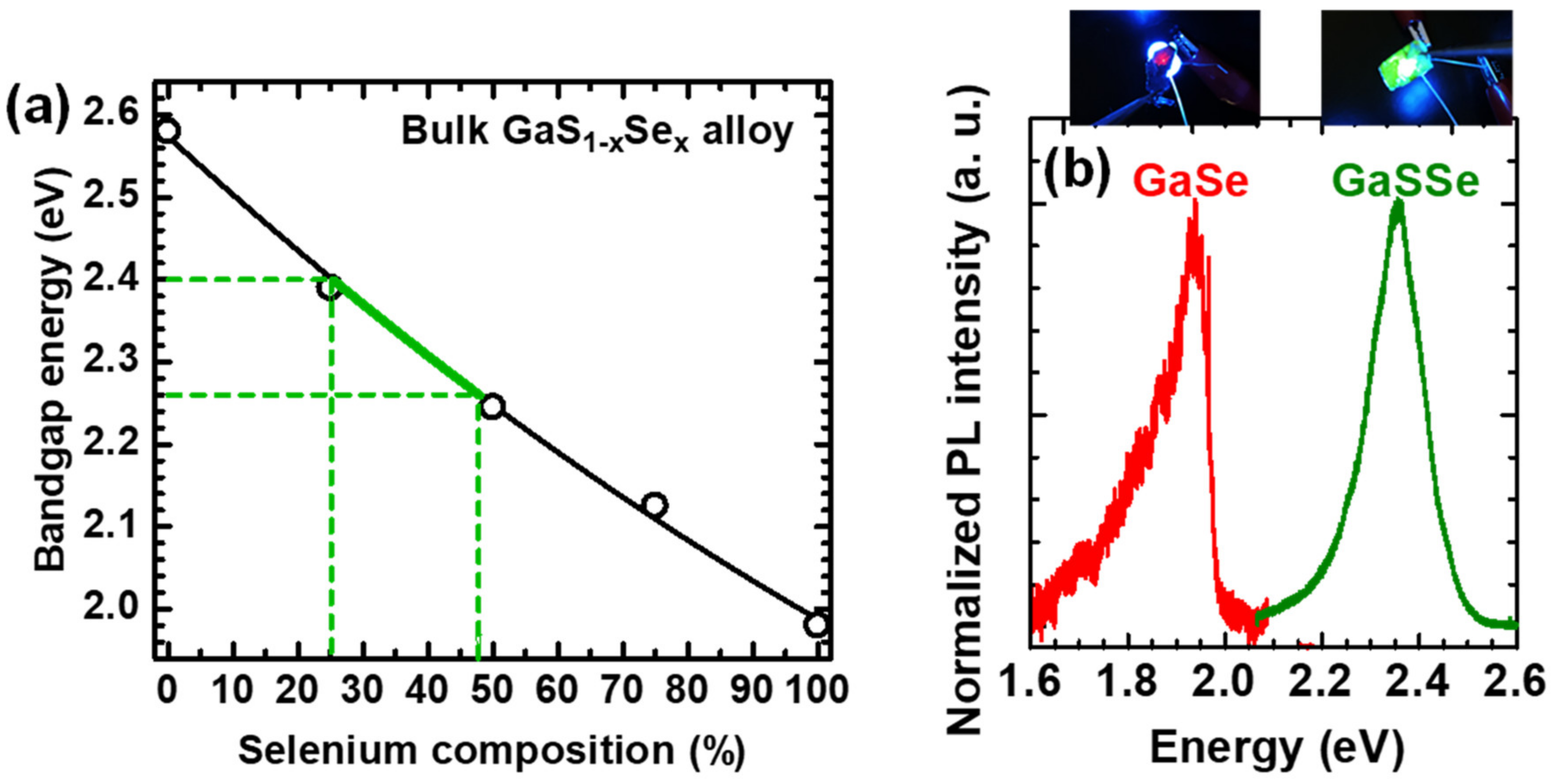
Layered GaS1−xSex alloys categorizing into III-VI materials show the energy bandgap bowing between 1.98 and 2.58 eV with the tuning of composition x, as shown in Figure 2a. This characteristic was estimated by fitting a quadratic function using the reported bandgap energy of compositions x (0%, 25%, 50%, 75% and 100%) [16]. When the composition is controlled between 25% and 48%, green-color luminescence with bandgap energy between 2.40 and 2.26 eV can be realized, respectively. In addition, red-color luminescence can be obtained with the composition x = 100%, which represents pure GaSe. Therefore, we adopted layered GaS1−xSex alloys as the emission-color converters of GaN-based blue μLEDs.
In this study, the compositions of S and Se for GaS1−xSex for green luminescence were set to 65% and 35%, respectively. XRD profiles of GaS0.65Se0.35 and GaSe bulk films are indicated the orientation along [001] direction. (Figure S1). Additionally, no phase separation was obtained in GaS0.65Se0.35 bulk film. Figure 2b shows the PL spectra of GaS0.65Se0.35 and GaSe bulk films. Peak energies of 2.36 and 1.94 eV were achieved from GaS0.65Se0.35 and GaSe, respectively. The full-width half-maximums (FWHMs) for PL spectra of GaS0.65Se0.35 and GaSe were 129 and 110 meV, respectively. The large FWHMs were affected through phonon scattering because both direct and indirect transitions can occur in the band structures of these materials [17]. Additionally, for GaS0.65Se0.35, the occurrence of microscopic composition fluctuations that are Ga–S and Ga–Se condensations, resulting in the distribution of density of states near the band edge. This usually occurs for other disordered compound alloys, such as AlInGaN and ZnMgO [18,19]. On the other hand, background noise was detected in the PL spectrum of GaSe because the excitation efficiency using blue light is lower than that of GaS0.65Se0.35 owing to the large energy difference. The inset in Figure 2b clearly shows green and red PL images obtained through the irradiation of blue light. Therefore, color conversion from blue to green and red light was achieved using GaS0.65Se0.35 and GaSe, respectively, suggesting that they are candidate materials for the emission-color converters of GaN-based blue μLEDs.
3.2. Demonstration of the Emission-Color Conversion of Blue μLED Utilizing GaS0.65Se0.35 and GaS Thin Films
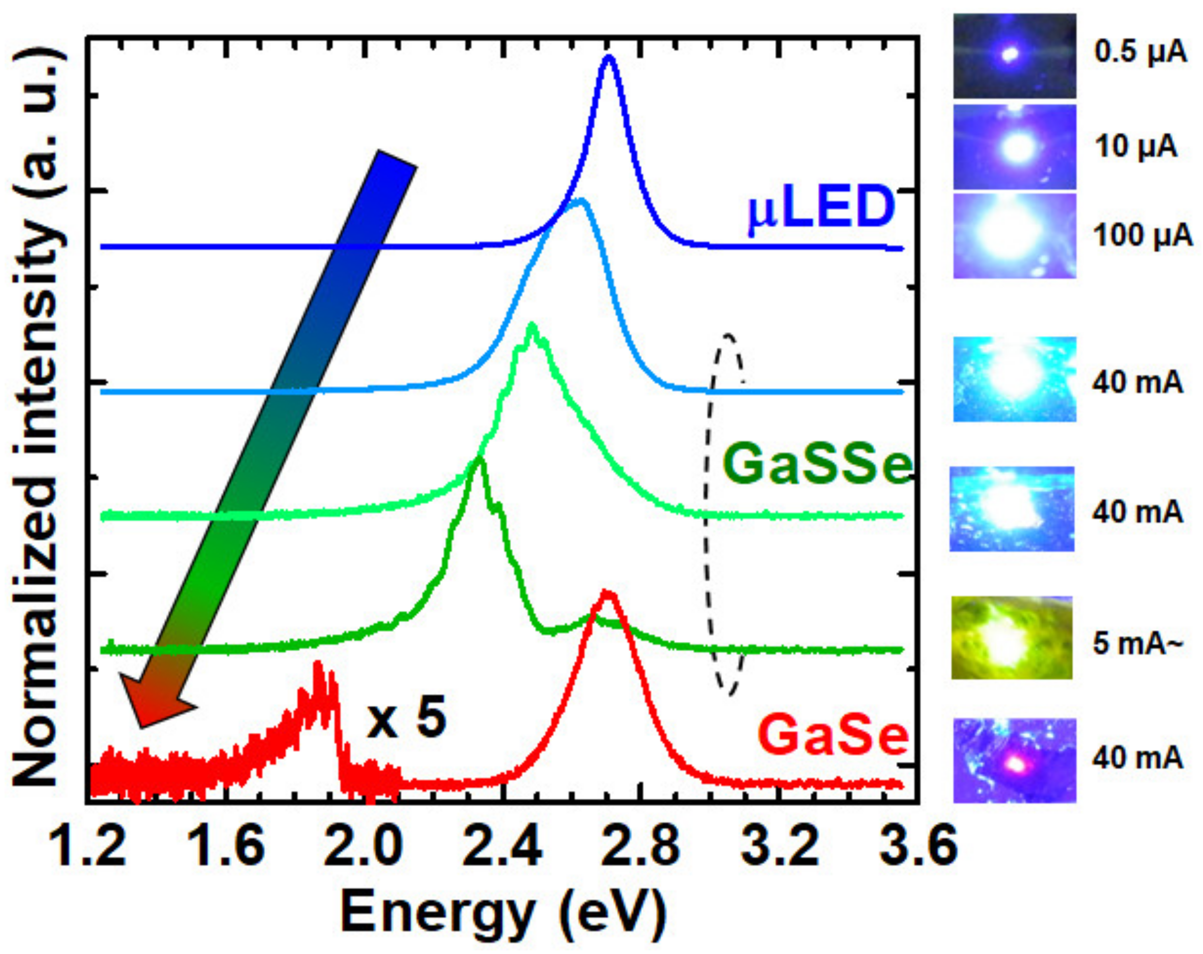
We conducted the emission-color conversion of the blue μLED chip through GaS0.65Se0.35 and GaSe thin films. Figure 3 shows the EL spectra of the μLED before and after the color conversion. The inset photographs show the EL images of the μLED before and after the color conversion. A luminescence peak was detected at 2.70 eV from the μLED before color conversion. Color-converted peaks were obtained between 2.32 and 2.60 eV by utilizing GaS0.65Se0.35 thin film with different layer thicknesses. The energy of the luminescence peak from the GaS0.65Se0.35 thin film was shifted toward the low-energy side with an increase in the thickness due to the increase in each layer interaction [20,21]. The low efficiency of color conversion was estimated to be below 1%. Weak luminescence at 1.88 eV was detected from color-converted μLED through a GaSe thin film. However, the excitation efficiency was low, as with the PL measurement shown in Figure 2b, leading to low efficiency of color conversion below 1%. This can be improved by designing a stacking-layer structure with stepped band alignment, such as double heterostructure with wide-bandgap barrier layers, which can enhance high-energy absorption. On the other hand, a part of the spectrum included the μLED peak at 2.70 eV as the excitation source owing to the spread and scattering of the blue light of the μLED. For applications of display and optogenetics, the improvement of light directivity is necessary using an integrated microlens. These results suggest the possibility of emission-color conversion of blue μLED chips utilizing layered materials. In this study, the thicknesses of layered GaSSe alloys as color converters were below 100 μm, which are slightly thinner than phosphors in the previous method. For future work, the thickness expects to be ultimately reduced to the order of few tens nm by using a superlattice consisting of monolayer sheets.
4. Conclusions
Layered materials have several advantages over other color converters, such as direct formation onto μLED chips and thin formation by designing a stacked-layer structure. This paper proposed the emission-color conversion of GaN-based μLEDs from blue to green and red emissions by utilizing layered materials, and presented its proof of concept. Layered GaS1−xSex alloys can show energy bandgap bowing within the visible light range and its luminescence. The PL of GaS0.65Se0.35 and GaSe can be achieved using blue light as the excitation source with the output level of the LED. Emission-color conversions were realized from blue to cyan, green, and red by directly utilizing the arranged GaS0.65Se0.35 and GaSe thin films onto GaN-based μLEDs.
Supplementary Materials
The following are available online at https://www.mdpi.com/2079-6412/10/10/985/s1, Figure S1: symmetrical XRD profiles of GaS0.65Se0.35 and GaSe bulk. Figure S2: Device structure of LED, J-L-V characteristics and external quantum efficiency of blue μLEDs.
Author Contributions
Conceptualization, N.U. and Y.H.; methodology, Y.T. and N.U.; validation, Y.T. and N.U.; investigation, Y.T. and N.U.; resources, N.U.; data curation, Y.T. and N.U.; writing—original draft preparation, N.U.; writing—review and editing, N.U. and Y.H.; supervision, Y.H.; project administration, N.U.; funding acquisition, N.U. All authors have read and agreed to the published version of the manuscript.
Funding
This research was funded by the Urakami Scholarship Foundation and the Shinshu University Manufacturing Promotion Association. Both grants are for 2019, and no numbers have been assigned.
Acknowledgments
A part of this work was carried out using the analysis facilities at the Global Aqua Innovation Center (AICS) at Shinshu University.
Conflicts of Interest
The authors declare no conflict of interest.
References
- Wu, T.; Sher, C.-W.; Lin, Y.; Lee, C.-F.; Liang, S.; Lu, Y.; Chen, S.-W.H.; Guo, W.; Kuo, H.-C.; Chen, Z. Mini-LED and Micro-LED: Promising Candidates for the Next Generation Display Technology. Appl. Sci. 2018, 8, 1557. [Google Scholar] [CrossRef] [Green Version]
- Huang, Y.; Ten, G.; Gou, F.; Li, M.-C.; Lee, S.-L.; Wu, S.-T. Prospects and challenges of mini-LED and micro-LED displays. J. Soc. Inf. Display 2019, 27, 387–401. [Google Scholar] [CrossRef]
- Lee, H.E.; Shin, J.H.; Park, J.H.; Hong, S.K.; Park, S.H.; Lee, S.H.; Lee, H.H.; Kang, I.-S.; Lee, K.J. Micro Light-Emitting Diodes for Display and Flexible Biomedical Applications. Adv. Funct. Mater. 2019, 29, 1808075. [Google Scholar] [CrossRef]
- Chen, K.-J.; Chen, H.-C.; Tsai, K.-A.; Lin, C.-C.; Tsai, H.-H.; Chien, S.-H.; Cheng, B.-S.; Hsu, Y.-J.; Shih, M.-H.; Tsai, C.-H.; et al. Resonant-Enhanced Full-Color Emission of Quantum-Dot-Based Display Technology Using a Pulsed Spray Method. Adv. Funct. Mater. 2012, 22, 5138–5143. [Google Scholar] [CrossRef]
- Han, H.-V.; Lin, H.-Y.; Lin, C.-C.; Chong, W.-C.; Li, J.-R.; Chen, K.-J.; Yu, P.; Chen, T.-M.; Chen, H.-M.; Lau, K.-M.; et al. Resonant-enhanced full-color emission of quantum-dot-based micro LED display technology. Opt. Express 2015, 23, 32504–32515. [Google Scholar] [CrossRef]
- Chen, G.-S.; Wei, B.-Y.; Lee, C.-T.; Lee, H.-Y. Monolithic Red/Green/Blue Micro-LEDs With HBR and DBR Structure. IEEE Photon. Technol. Lett. 2018, 30, 262–265. [Google Scholar] [CrossRef]
- Tao, T.; Zhi, T.; Cen, Z.; Liu, B.; Wang, Q.; Xie, Z.; Chen, P.; Chen, D.; Zhou, Y.; Zheng, Y.; et al. Hybrid Cyan Nitride/Red Phosphors White Light-Emitting Diodes With Micro-Hole Structure. IEEE Photon. J. 2018, 10, 8201608. [Google Scholar] [CrossRef]
- Gou, F.; Hsiang, E.-L.; Tan, G.; Lan, Y.-F.; Tsai, C.-Y.; Wu, S.-T. High performance color-converted micro-LED displays. J. Soc. Inf. Display 2019, 27, 199–206. [Google Scholar] [CrossRef]
- Wang, Z.; Shan, X.; Cui, X.; Tian, P. Characteristics and techniques of GaN-based micro-LEDs for application in next-generation display. J. Semicond. 2020, 41, 041606. [Google Scholar] [CrossRef]
- Haase, M.A.; Xie, J.; Ballen, T.A.; Zhang, J.; Hao, B.; Yang, Z.H.; Miler, T.J.; Sun, X.; Smith, T.L.; Leatherdale, C.A. II-V-semiconductor color converters for efficient green, yellow, and red light emitting diodes. Appl. Phys. Lett. 2010, 96, 231116. [Google Scholar] [CrossRef]
- Santos, J.M.M.; Jones, B.E.; Schlosser, P.J.; Watson, S.; Herrnsdorf, J.; Guihabert, B.; McKendry, J.J.D.; Jessus, J.D.; Garcia, T.A.; Tamargo, M.C.; et al. Hybrid GaN LED with capillary-bonded II-VI MQW color-converting membrane for visible light communications. Semicond. Sci. Technol. 2015, 30, 035012. [Google Scholar] [CrossRef] [Green Version]
- Butler, S.Z.; Hollen, S.M.; Cao, L.; Cui, Y.; Gupta, J.A.; Gutiérrez, H.R.; Heinz, T.F.; Hong, S.S.; Huang, J.; Ismach, A.F.; et al. Progress, Challenges, and Opportunities in Two-Dimensional Materials Beyond Graphene. ACS Nano 2013, 7, 2898–2926. [Google Scholar] [CrossRef] [PubMed]
- Ponraj, J.S.; Xu, Z.-Q.; Dhanabalan, S.C.; Mu, H.; Wang, Y.; Yuan, J.; Li, P.; Thakur, S.; Ashrafi, M.; Mccoubrey, K.; et al. Photonics and optoelectronics of two-dimensional materials beyond graphene. Nanotechnology 2016, 27, 462001. [Google Scholar] [CrossRef] [PubMed]
- Mueller, T.; Malic, E. Exciton physics and device application of two-dimensional transition metal dichalcogenide semiconductors. NPJ 2D Mater. Appl. 2018, 2, 29. [Google Scholar] [CrossRef] [Green Version]
- Thakar, K.; Lodha, S. Optoelectronic and photonic devices based on transition metal dichalcogenides. Mater. Res. Express 2020, 7, 014002. [Google Scholar] [CrossRef]
- Isik, M.; Gasanly, N. Composition-tuned band gap energy and refractive index in GaSxSe1−x layered mixed crystals. Mater. Chem. Phys. 2017, 190, 74–78. [Google Scholar] [CrossRef]
- Jung, C.S.; Park, K.; Shojaei, F.; Oh, J.Y.; Im, H.S.; Lee, J.A.; Jang, D.M.; Park, J.; Myoung, N.; Lee, C.-L.; et al. Photoluminescence and Photocurrents of GaS1−xSex Nanobelts. Chem. Matter. 2016, 28, 5811–5820. [Google Scholar] [CrossRef]
- Kazlauskas, K.; Tamulaitis, G.; Žukauskas, A.; Khan, M.A.; Yang, J.W.; Zhang, J.; Simin, G.; Shur, M.S.; Gaska, R. Double-scaled potential profile in a group-III nitride alloy revealed by Monte Carlo simulation of exciton hopping. Appl. Phys. Lett. 2003, 83, 3722–3724. [Google Scholar] [CrossRef] [Green Version]
- Laumer, B.; Wassner, T.; Schuster, F.; Stutzmann, M.; Schörmann, J.; Rohnke, M.; Chernikov, A.; Bornwasser, V.; Koch, M.; Chatterjee, S.; et al. Exciton confinement in homo- and heteroepitaxial ZnO/ZnMgO quantum wells with x <0.1. J. Appl. Phys. 2011, 84, 093513. [Google Scholar] [CrossRef] [Green Version]
- Del Pozo-Zamudio, O.; Schwarz, S.; Sich, M.; Akimov, I.A.; Bayer, M.; Schofield, R.C.; Chekhovich, E.A.; Robinson, B.J.; Kay, N.D.; Kolosov, O.V.; et al. Photoluminescence of two-dimensional GaTe and GaSe films. 2D Mater. 2015, 2, 035010. [Google Scholar] [CrossRef]
- Jung, C.S.; Shojaei, F.; Park, K.; Oh, J.Y.; Im, H.S.; Jang, D.M.; Park, J.; Kang, H.S. Red-to-Ultraviolet Emission Tuning of Two-Dimensional Gallium Sulfide/Selenide. ACS Nano 2015, 9, 9585–9593. [Google Scholar] [CrossRef] [PubMed]
Figure 1.
(a) Schematic diagrams of a conventional method for emission-color conversion of gallium nitride (GaN)-based micro light-emitting diodes (μLEDs) from blue to green and red. Phosphors and quantum dots (QDs) as color converters can be directly coated on GaN-based μLEDs. The thicknesses of phosphorus and QDs are approximately 100 and 10 μm, respectively. II-VI based quantum wells (QWs) are placed on GaN-based μLEDs through a transparent carrier substrate (glass or quartz). Total thickness of QWs structure is below 5 μm, however, the carrier substrate is at least 200 μm. (b) Schematic diagram of our proposal for emission-color conversion of GaN-based μLEDs from blue to green and red. Additionally, layered materials can be directly placed on GaN-based μLEDs. The thickness of layered materials is below 100 μm in this work. For future work, the thickness expects to be ultimately reduced to the order of a few tens nm.
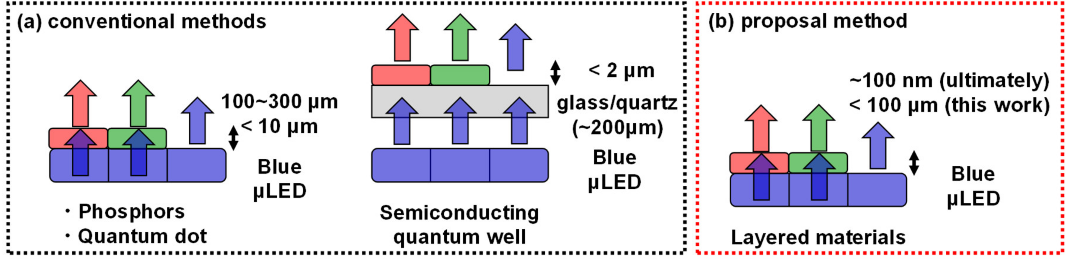
Figure 2.
(a) Sulfur (S) and selenium (Se) composition dependence of bandgap energy for layered GaS1−xSex alloy. The bandgap energy covering the green emission is realized with the Se of composition x between 25% and 48%. The red emission is achieved by GaSe (x ~ 100%). (b) Photoluminescence (PL) spectra of GaS0.65Se0.35 and GaSe films using blue LED as an excitation source. The inset photographs provide PL images of GaS0.65Se0.35 and GaSe films. The thicknesses GaSSe and GaSe were 400 and 150 μm.

Figure 3.
Electroluminescence (EL) Spectra of GaN-based μLED chips with and without GaS0.65Se0.35 and GaSe thin films as green and red converters. The inset photographs show EL images of μLED chips with GaS0.65Se0.35 and GaSe films. The thicknesses were 44, 60 and 98 μm for GaSSe, and 72 μm for GaSe.
Publisher’s Note: MDPI stays neutral with regard to jurisdictional claims in published maps and institutional affiliations. |
© 2020 by the authors. Licensee MDPI, Basel, Switzerland. This article is an open access article distributed under the terms and conditions of the Creative Commons Attribution (CC BY) license (http://creativecommons.org/licenses/by/4.0/).
Share and Cite
MDPI and ACS Style
Tsuboi, Y.; Urakami, N.; Hashimoto, Y. Photoluminescence of Layered Semiconductor Materials for Emission-Color Conversion of Blue Micro Light-Emitting Diode (µLED). Coatings 2020, 10, 985. https://doi.org/10.3390/coatings10100985
AMA Style
Tsuboi Y, Urakami N, Hashimoto Y. Photoluminescence of Layered Semiconductor Materials for Emission-Color Conversion of Blue Micro Light-Emitting Diode (µLED). Coatings. 2020; 10(10):985. https://doi.org/10.3390/coatings10100985
Chicago/Turabian StyleTsuboi, Yuma, Noriyuki Urakami, and Yoshio Hashimoto. 2020. "Photoluminescence of Layered Semiconductor Materials for Emission-Color Conversion of Blue Micro Light-Emitting Diode (µLED)" Coatings 10, no. 10: 985. https://doi.org/10.3390/coatings10100985
Note that from the first issue of 2016, this journal uses article numbers instead of page numbers. See further details here.