Article

Meyer-Rod Coated 2D Single-Crystalline Copper Nanoplate Film with Intensive Pulsed Light for Flexible Electrode

1
Graduate school of Flexible and Printable Electronics, Jeonbuk National University, Jeonju 54896, Korea
2
Advanced Manufacturing Systems Research Division, Korea Institute of Machinery and Materials (KIMM), 156 Gajeongbuk-Ro, Yuseong-Gu, Daejeon 34103, Korea
3
Department of Chemistry and Chemical Engineering, Inha University, Incheon 22212, Korea
4
School of Integrative Engineering, Chung-Ang University, Seoul 06974, Korea
5
Graduate school of Flexible and Printable Electronics, LANL-JBNU Engineering Institute-Korea, Jeonbuk National University, Jeonju 54896, Korea
*
Authors to whom correspondence should be addressed.
These authors contributed equally to this work.
Coatings 2020, 10(1), 88; https://doi.org/10.3390/coatings10010088
Submission received: 29 November 2019 / Revised: 10 January 2020 / Accepted: 16 January 2020 / Published: 20 January 2020
(This article belongs to the Special Issue UV-Curable Coatings for Flexible/Wearable Electronics)

Abstract

:
Copper is widely used because it is inexpensive, abundant, and highly conductive. However, most copper used in industrial coating processes is in the form of circular powder, which is problematic for large area, high conductive coatings. In this work, 2D single-crystalline Cu nanoplates (Cu NPLs) were synthesized and a systematic study on coating with large-scale Cu NPLs using a Meyer-rod coating process was performed. The rheological behaviors of the Cu solution with various concentrations, surface tensions, and speeds were analyzed using Ca and Re numbers to optimize coating conditions. In addition, the effect of intensive pulse light (IPL) to sinter the coper film within a 1 s timeframe was also investigated in order to be able to produce an electrode in the shortest possible time which is applicable to industry. Finally, the Meyer-rod coated electrode was utilized in an electrochemical luminescence (ECL) device.

Graphical Abstract

1. Introduction

Metal nanoparticles are attractive thanks to their suitability in a wide variety of fields such as optoelectronics, catalysis, magnetics, microelectronic, and biotechnological applications [1,2,3,4,5,6]. Among these, copper is seen as promising because it is inexpensive, abundant, and highly conductive. As the nanoparticle size is a particularly important factor in improving the activity or functionality for practical applications, various synthetic methods have been introduced and a potential growth mechanism has been proposed that allows us to investigate the relationship between the crystal structure and the physical, optical, and electrical functionalities. Recently, Fan et al. synthesized 4 µm 2D (two-dimensional) Cu nanocrystals using polyethylene glycol as a capping agent [1]. However, achieving a well-defined, eco-friendly, simple, and dimension-controlled synthesis of Cu NPLs for potential electronic ink applications, particularly for a size of tens microns, has not been fully researched. To achieve these demands, we previously demonstrated a simple method for Cu nanocrystals with large dimension from nanowires (NWs) (1D) to nanoplates (NPLs) (2D) by adding iodine (I). The combination of an additive (iodine (I)), mild reductant (glucose), stabilizer (hexadecylamine, HDA), and reaction time produced large single-crystalline 2D Cu NPLs with edge lengths up to 30 µm [7].
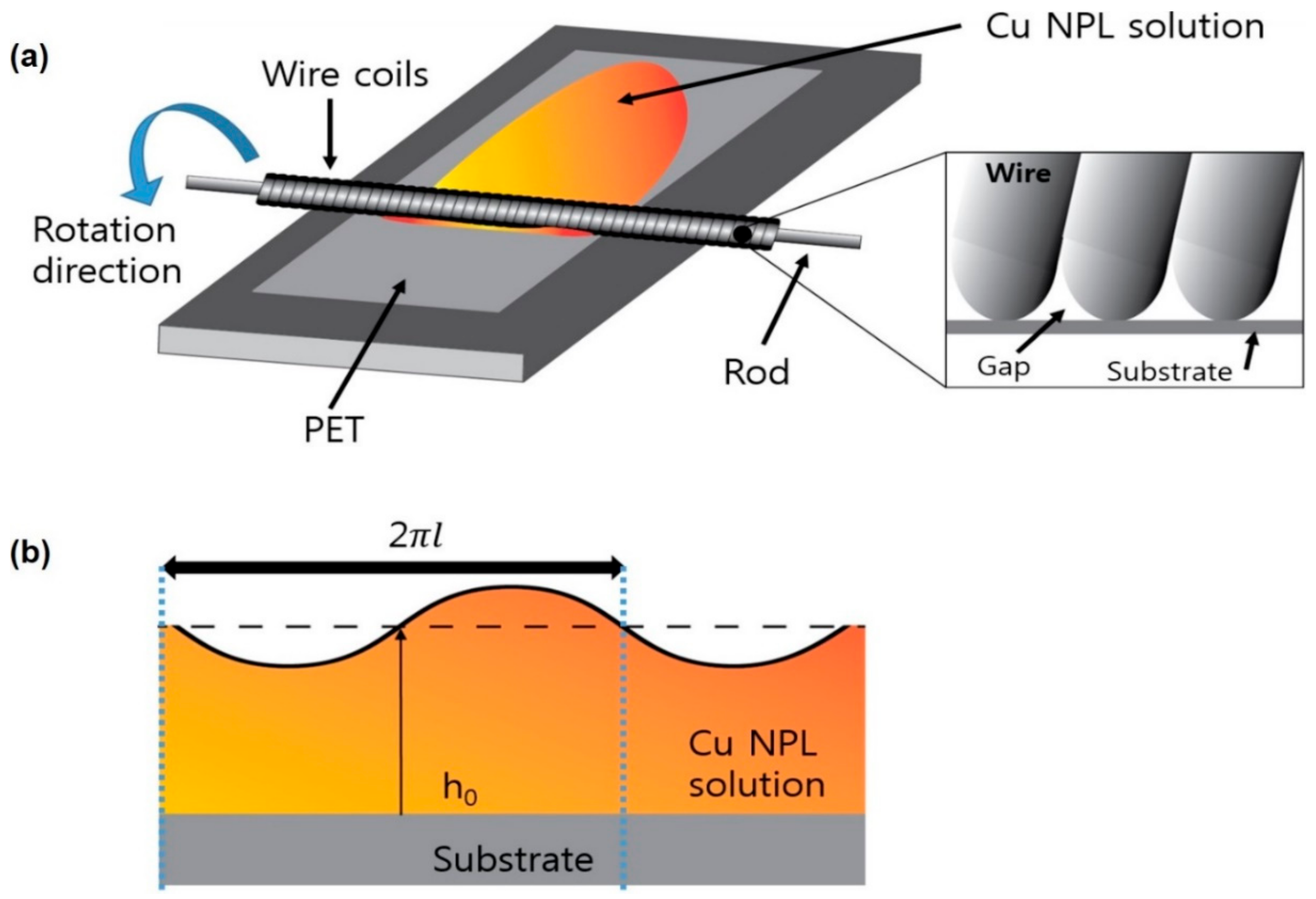
Recently, flexible and stretchable electronic devices, defined as soft electronics, have been dramatically attractive to replacing conventional rigid applications [8]. Meyer-rod coating (rod coating) is a well-known coating process used in the coating industry for fabrication of flexible and conductive film owing to its structural simplicity and ease of scaling up [8,9,10,11,12]. In addition, the coating solution suitable for this technology is easily ported to other high mass production methods such as slot die coating and roll coating. An important aspect ratio in rod coating is the formulation of a coating fluid with specific rheological behavior and wetting properties, which are largely dependent on viscosity and surface tension [13,14,15,16,17]. For colloidal suspensions, especially, enough solids should be contained in the fluid to form uniform and continuous layers during the drying process. Although various copper-based materials are used in the method mentioned above, use of large-scale 2D single-crystalline Cu nanoplates (NPLs) to fabricate film in the rod coating process has not been reported. Figure 1a shows a schematic diagram of the Meyer-rod coating process set up in this work to deposit the synthesized Cu NPL solutions. The homogeneous Cu NPL solution passes through the gaps when the body of the metal rod is drawn over the solution. In that moment, a series of strips are found on the coated solution according to the shape of the wires, and the solution is separated by the spacing of the wire windings. Then, the strips are separated by a certain distance, start to level, and spread owing to surface tension of the coating’s pulling action. At the same time, the viscosity of the Cu NPL slows down the leveling process, which results in the uniform formation of a film that does not have serious defects caused by any secondary flow effect. Before the coating is dry, this achievement of proper leveling (disappearing of the strips) is critical to obtain a uniform coating surface. To quantify the efficiency of the leveling process, dimensional numbers—the Capillary ( C a = μ ν / σ , Ca) and Reynolds ( R e = ρ ν l / μ , Re) number, where μ is the viscosity of the fluid, ν is the characteristic velocity, σ is the surface tension, ρ is the fluid density, and 2 π l is the wavelength of a sinusoidal disturbance [2]—are generally utilized. These numbers express the dominant effects of surface tension and viscosity as the driving forces of the leveling process. Once the fluid is set in motion, right after the rod is submerged, as shown in Figure 1b, the surface tension between the convex and concave regions of the wavy fluid induces a capillary leveling, which is maintained by inertial forces (oscillations). Then, the viscous force weakens the leveling process by distributing the fluid momentum through the entire film thickness. Thus, a low Ca number indicates that capillary force dominates viscous force, driving the leveling process, whereas a high Re number indicates that viscous force dominates inertial force, diminishing the oscillation effect. An analysis of the coating process with Ca and Re numbers is covered in a later section. To form a uniform film, based on the discussion above, the leveling time [1] can be estimated as t l e v e l = 3 μ 1 l 4 / σ h 03 , where μ 1 ,   σ   and   h 0 are the high-shear viscosity of the Cu NPL solution, surface tension, and average thin film thickness, respectively. This leveling time has to be short enough so that the drying time t d r y i n g = h o / J o , where Δ h and J o are the thickness of the liquid layer and solvent evaporation current (cm/s), respectively—allows the strips to merge together.
Recently, a light-emitting device, based on the electrochemical luminescence (ECL) phenomenon, has attracted great attention as a new type of organic light-emitting device (OLED). Although OLED technology has made great strides based on the continuous efforts of research institutes around the world, the excessive air sensitivity of constituent electrodes and light emitting materials as well as the passivation of devices and chemical orthogonality between materials according to the laminated structure of those materials are still problematic areas. On the other hand, ECL-based light emitting devices are not only insensitive to moisture and air, but also relatively free from problems such as the shape of the interlayer structure and the uniformity in thickness of the active layer.
In this work, we systematically investigated the coating of large-scale 2D single-crystalline Cu NPLs, which were synthesized by a simple hydrothermal method with Meyer-rod coating process, and sintered them with intensive pulse light (IPL) system for soft electronics. To understand the coating mechanism of 2D Cu NPLs, the rheological behavior of the Cu solution was analyzed regarding surface tension, so that proper conditions for a uniform coating were achieved in terms of the Ca and Re numbers. In addition, we systematically investigated the effect of intensive pulse light (IPL) to sinter the coper film within a 1 s timeframe, in which the change in sheet resistance according to the applied energy on the coated 2D Cu NPLs was measured. XRD measurements to find the effect of coating thickness and concentration of the Cu ingredients were also performed. For an example application, the produced Meyer-rod coated 2D Cu NPLs were used as electrodes for an electrochemical luminescence (ECL) device.

2. Experiment

2.1. Materials and Methods

Materials. Copper (II) chloride dihydrate (CuCl2.2H2O, purity 99+%), hexadecylamine (HDA), glucose (purity 99.5+%), Tris (bipyridine) ruthenium (II) chloride (Ru (bpy) 3Cl2 (purity: 99.7%)), poly (vinylidene fluoride-co-hexafluoropropylene), (PVDF-HFP, Mw = 130,000 g mol1), and 1-Ethyl-3-methylimidazolium bis (trifluoromethylsulfonyl) imide and [EMIM][TFSI] were purchased from Sigma-Aldrich, St. Louis, MO, USA. Acetone was procured from Samchun pure chemical. All the chemical and reagents were of analytical grade and were used directly without any further purification.

2.2. Preparation of Cu Plate Ink

Copper (||) chloride dihydrate (CuCl2∙2H2O, 99+%) (6.3 mg mL−1), HDA (98%) (73.2 mg mL−1), and glucose (99.5+%) (15 mg mL−1) were dissolved in deionized water (DI) water (150 mL). The solution was mixed for 3 min at room temperature by blender mixing machine, and the mixture was put into a Teflon-lined autoclave. Then, the Teflon-lined autoclave was kept in an oil bath at 100 °C and stirred for 6 h. After the reaction, the color of the mixture solution changed from blue to reddish brown, resulting in the production of Cu nanowires (Cu NWs). After that, a very small amount of iodine (I2, 99.8+%) (4.72 mg) was added in the same composition to the mixture solution for Cu NWs. The mixture solution was reacted in the same type of Teflon-lined autoclave at 100 °C and stirred for 12 h. The reactant solutions were washed in chloroform and DI water several times using a centrifuge, producing Cu nanoplates [7]. To make the Cu nanoplate solution, mixing the Cu nanoplates with an organic solvent containing acetone (3.7 mL), ethanol (3.8 mL), ethyl acetate (1.75 mL), isopropyl alcohol (IPA) (5 mL), and toluene (2 mL) was undertaken.

2.3. Preparation of Ion Gel for ECL Device

A co-dissolution synthesis method was used for the preparation of ion gel solution using Ru(bpy)3Cl2, P(VDF-HFP), and [EMIM][TFSI] in acetone. The weight ratio of the solvent, ionic liquid, and polymer was kept at 7:4:1. The concentration of Ru (bpy) 3Cl2 was 10 wt% for the purpose of ECL device performance. The solution was stirred for 2 h at room temperature. Finally, a gel type ion solution for the ECL device was produced [18].

2.4. Fabrication of Cu NPL Film and ECL Device with Performance

Various concentrations of Cu NPL solution were loaded into the Meyer-rod coating machine (13 mm dia., 240 μm mil wire) where the coating speed was fixed at 2 cm/sc. Then, the coated film was sintered using Pulse Forge 1300 IPL machine equipped with xenon flash lamp for 1–3 sec at 1–2.1 J/cm2. Finally, an ECL device was fabricated using a simple drop casting process of ion gel ink onto a Cu NPL substrate film, which is used as a bottom electrode after drying ink gel ink in ambient conditions overnight to remove the residual solvent. A transparent indium tin oxide (ITO) coated polyethylene terephthalate (PET) film was used as a top electrode for the ECL device. The thickness of the coated ion gel onto Cu NPL substrate was measured to be ~450 μm and the fabricated ECL device was laminated properly with PET film to avoid air passage and any other means of contamination to the ECL device. For measuring the ECL device performance, the Tektronix AFG 1022 arbitrary function generator was used. The fabricated ECL device can be operated at low voltage under an Alternating current (AC) bias voltage of 3.4 V (peak to peak voltage) with a frequency of 5 Hz.

2.5. Characterization

The ink rheology behavior of the Cu NPL was examined using an ink hybrid rheology-meter (Discovery hr-3, Delaware, USA); the initial structural was confirmed using an optical microscope (Nikon, Tokyo, Japan, ECLIPSE, LV-100ND) with leopard 2.6 software; the morphology and microstructure of the Cu NPL was characterized using scanning electron microscopy (JIB-4601F, JEOL, Tokyo, Japan); and finally the crystal structure, phase purity, and lattice parameters of the Cu NPL were analyzed by X-ray diffraction (BRUKER, D8 Advance, Karlsruhe, Germany) using CuKα radiation. The electrical properties of the film were examined by four probe (Keithley, Model: 2420, Seoul, Korea) technique dc conductivity measurements for obtaining the sheet resistance.

3. Result and Discussion

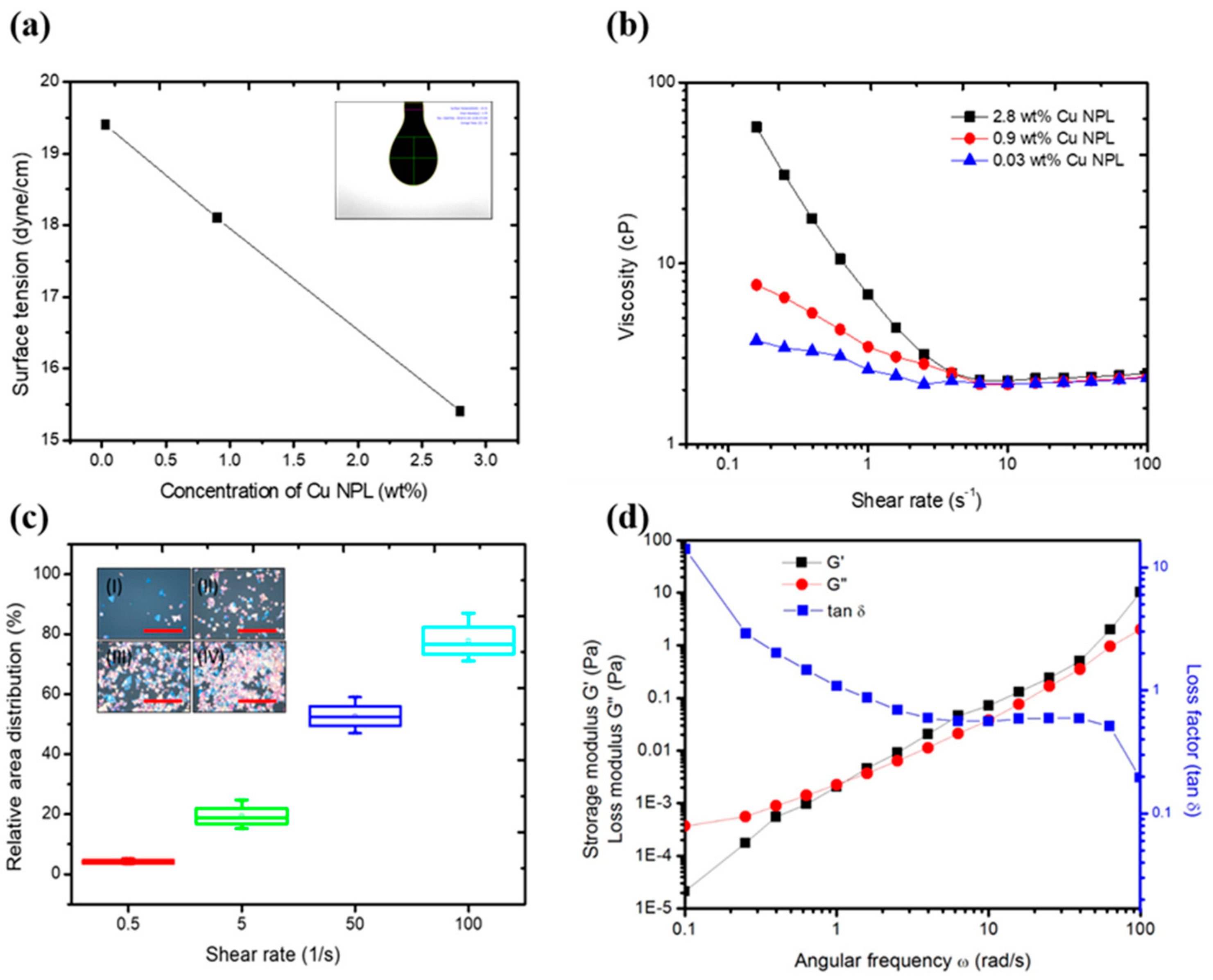
In general, when the coating solution is spread out, the area of coated film is reduced as a result of surface tension, which can cause severe defects such as dewetting and fisheyes [4]. Thus, surface tension is a vital factor in the coating process that determines the wettability of the coating solution. One of the factors influencing the surface tension is the quantity of nanoplates in the solution. Figure 2a reveals that an increase in the amount of Cu NPLs from 0.03 wt%, 0.9 wt%, and 2.8 wt% induced a decrease in the surface tension from 19 to 15 dyne/cm, which may be attributed to the Brownian motion and adsorption of the nanoplates at the interfaces [5]. On the other hand, polyvinylpyrrolidone (PVP) plays an important role as a surfactant for the Cu plate coating solution [6], and surface tension with various PVP concentrations such as 0.2, 1 mM, and 3 mM PVP was measured. However, all these surface tension measurements had similar values of around 17 dyne/cm, which is similar to the tendency found by Chen et al. [19]. In addition, PVP is known as a dispersing agent that keeps the coating solution from flocculating. However, a higher PVP concentration degrades electrical performance owing to the intrinsically insulating properties of PVP itself [1]. So, in this work, 1 mM PVP was chosen as the best ratio to formulate our Cu NPL solution.
Next, the rheological behavior of Cu NPL solution with various Cu NPL concentration was investigated to understand the leveling process of the bar-coated Cu NPL solutions. Figure 2b shows the results of our steady state flow test for 0.03 wt%, 0.9 wt%, and 2.8 wt% Cu plate solution as a function of shear rate (s−1). All the coating solutions reveal similar shear thinning behavior; as the shear rate increases gradually, the Cu NPL structure loses its recoverability, and the interaction between Cu NPLs is weakened, resulting in the presence of shear thinning behavior. As a higher concentration indicates a higher packing effect of the Cu NPLs, which in turn induces a stronger electrostatic interaction between NPLs, the viscosity at the zero-shear rate (or low shear rate) was proportionally increased with increases in concentration; for viscosities of 2.8 wt%, 0.9 wt%, and 0.03 wt%, the shear rates were 56, 7.6, and 3.7 cp at 0.1 s−1, respectively. The non-Newtonian characteristics of Cu NPL depending on shear rate are in accordance with the coating fluid [20,21], which is especially true for copper-based coating solutions [4,5,22,23]. Furthermore, to investigate how the speed of the bar coating process affects coating uniformity, the 2.8 wt% Cu NPL solution was applied with various coating speeds corresponding to applied shear rates. The shear rates were simply calculated by coating speed divided by unit length of coating (0.2 mm). Figure 2c illustrates the relative area distribution (RAD) obtained for 0.1, 1, 10, and 20 mm/sec coating speeds, which correspond to shear rates of 0.5, 5, 50, and 100 s-1, respectively. Here, RAD can be explained as how much is covered by the Cu NPLs in a certain unit area on PET. As coating speed increased (or shear rate increased), the RAD of the Cu NPLs was proportionally increased from 4.1% to 77.7% for 0.5 and 50 s−1 at a given coated area, respectively. This increase in RAD with raising shear rate can be attributed to an increase in wet film thickness during the coating process, allowing more deposition and movement of the Cu NPLs [21,24]. This tendency agrees well with the results of the shear thinning behavior shown in Figure 2b. At low shear rates, the Cu NPL solution behaved in a more solid-like manner and responded easily to the rod coater being drawn down, which resulted in the Cu NPLs being displaced by the moving rod, leaving only a small number of particles on PET. At high shear rates (high coating speed), the fluid behaved in a more fluid-like manner and responded less to the moving rod, resulting in leaving a larger amount of Cu NPLs on PET. The insets show photographs of the coated Cu NPLs on PET with shear rates of 0.5 (I), 5 (II), 50 (III), and 100 (IV). The viscoelastic effect explains the interactions among particles when it reaches its critical point. To observe these viscoelastic effects, a frequency sweep test of 2.8 wt% Cu NPL solution was also carried out under 0.1 of strain in the viscoelastic region. In Figure 2d, the curves of storage modulus and G′(elastic) as well as loss modulus and G″(viscous) for the solution are plotted; in these, we can see a slightly higher G′ than G″ was observed when G′ and G″ intersected at the critical point of 1 ω , both increased as a function of ω . The reason for dominance of G′ over the critical point at low frequency is attributed to a tightly packed dispersion system caused by the large aspect ratio of Cu NPL (thickness/length = 200). Also, the intensity of the viscoelastic behavior can be characterized by measuring tan δ , the ratio of viscous to elastic behavior, which was 2.89 for 2.8 wt% Cu NPL solution. In general, a coating solution with tan δ < 1 indicates a highly ordered structure owing to tightly packed molecules under a weak force, while tan δ > 10 indicates a fluid like character, where the molecules are in disassembled form. For assembled thin film coating materials, an intermediate tan δ is necessary for uniform coating on the desired substrates [25]. Thus, 2.8 wt% Cu NPL solution shows the required existence of an assembled structure and is suitable for the Meyer-rod coating process.
On the basis of the surface tension and shear viscosity, Ca and Re numbers, leveling, and drying time, the different concentrations of Cu plate solution were calculated, as seen in Table 1. The average film thickness ( h 0 ) is assumed to be 20 µm according to 10% of the diameter of wire (0.2 mm). The drying time was 400 s, measured with a chronograph at room temperature. L and high shear viscosity were assumed to be 1 mm and 100 s−1, respectively. As seen in Table 1, the optimized condition of surface tension and viscosity for Cu NPL 2.8 wt% solution for achieving higher RAD was less than 20 mN/m and 2.4–56 mPa·s, respectively, resulting in Ca < 0.5 and Re > 1 at the 2 cm/s of printing speed. Although Re < 1 could be obtained at a 10 times lower speed to produce a more uniform coating in theory, a poor RAD ratio determining film thickness to achieve the desired electrical performance and higher productivity prohibits selecting this lower speed.
Using the IPL system, which is a millisecond process that minimizes the annealing cycle by using visible light with a broad spectrum, the Cu NPL 2.8 wt% solution on PET was sintered with various times and energies. Figure 3a indicates that sheet resistance was decreased with an increase in applied voltage with time, although further decreases in the sheet resistance were not observed for annealing times over 1 s. In addition, as seen in Figure 3b, the sheet resistance was inversely proportional to the applied energy, the threshold energy was found to be 2.1 J/cm2, and it produced the lowest sheet resistance of 1.2 ohm/sq. These results indicate that higher energy is more efficient for PVP decomposition and the necking of nanoplates. More importantly, using 2.1 J/cm2 of applied energy to obtain 1.2 ohm/sq is one order lower in terms of energy compared with the use for nanoparticle type Cu solution [26]. As the aspect ratio of the Cu NPL was 200, absorption of the irradiated light energy was more efficient, which induces the growth of neck-like junctions among Cu NPLs.
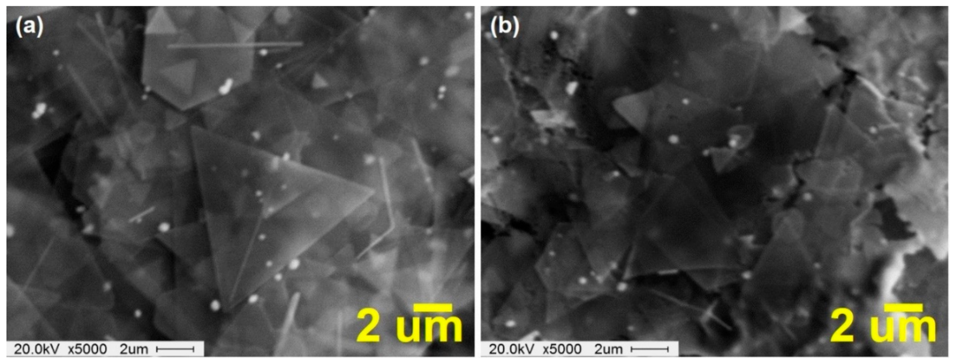
Figure 4a,b shows scanning electron microscope (SEM) images of Cu NPL solution before and after irradiation with energy of 2.1 J/cm2 for 1 ms, in which the amount of Cu coalescence is increased in comparison with Cu NPL.
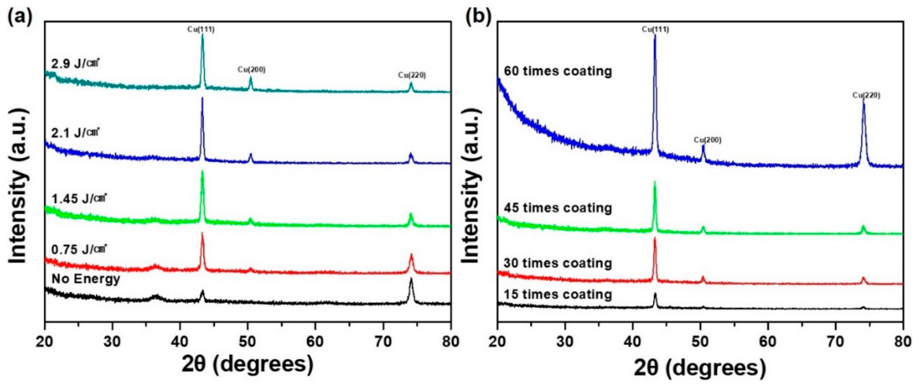
To investigate the crystal phase change of the oxide-covered copper nanoparticles compared with IPL sintered copper film, which affects film conductivity, X-ray diffraction measurements were taken at different energies applied by the IPL system. Figure 5a reveals that the characteristic peaks of the dry copper nanoparticles correspond to cuprous oxide [Cu2O, copper(I) oxide] 36.4, 42.3, and 61.3 and to face-centered cubic (FCC) pure copper phase 43.2, 50.4, and 74.1, respectively, according to existing references (Joint Committee on Powder Diffraction Standards (JCPDS) no. 01-1242). After higher IPL irradiation, the XRD peaks corresponding to Cu2O disappeared gradually and were completely removed when the energy reached to 2.1 J/cm2. On the basis of these observations, PVP had an oxide reduction function in the IPL sintering process [1]. Figure 5b shows the XRD analysis for various coating times for determining film thickness of the CU NPL solution. As expected, more coating of the Cu NPL solution tended to produce a higher intensity of the copper crystal phase when irradiated at 2.1 J/cm2 owing to a higher film thickness of the Cu NPL solution.
The mechanical flexibility of the Cu NPL coated flexible PET film was evaluated through the continuous bending test using a home-made bending test system. Figure 6a depicts the result the continuous 2000 cycles of bending test of Cu NPL coated flexible PET film under different strain. The change in resistance for Cu NPL coated PET film under bending test can be expressed as (ΔR = R − R0)/R0, where R is the measured resistance under bending state and R0 is the initial measured resistance. The following equation can be used to calculate the strain for Cu NPL coated flexible PET film:
Strain% = dCu NPL + d PET/2R,
where dCu NPL and dPET are the thicknesses of the Cu NPL layer and the PET substrate, respectively. Bending results tested under strain of 0.2%, 0.5%, and 1% with a bending radius of 0.2 mm, 0.4 mm, and 1 mm, respectively. As a result, no exceptional resistance change was observed until 0.5% (inset image). Figure 6b shows the practical application of Cu NPL film coated on PET as an electrode for an ECL device. In general, ECL devices are formed in a single active layer composed of a light emitting material and an electrolyte causing electrochemical oxidation/reduction between two opposing electrodes and light is generated through there. Compared with conventional OLED devices based on an organic multilayer thin film structure, this solution has various advantages such as a simple device structure, low drive voltage, low cost solution process, and an electrode independent of work function. In this case, the solution processed ECL device was realized using the Cu NPL film as the bottom electrode, as seen Figure 6c, resulting in fulfillment of required conductivity and flexibility for an ECL device; the inset image shows an image of the sintered Cu NPLs taken by microscope.
4. Conclusions

In this work, large-scale 2D single-crystalline Cu NPLs were synthesized by a simple hydrothermal method and coated to produce a conductive and flexible electrode. An ECL device was fabricated using the produced electrode for demonstration purposes. The rheological behaviors of the Cu solution were systematically investigated by looking at surface tension and copper concentration with coating speed and frequency sweep. In addition, critical dimensional numbers for coating such as Ca and Re numbers were utilized for a coating optimization analysis. After that, the effects of an IPL system used to sinter the coper film within a 1 s timeframe were systematically investigated, in which the change in sheet resistance with applied energy on the coated 2D Cu NPLs was measured. XRD measurements to investigate the effect of coating thickness and concentration of the Cu ingredients were also performed. As a sample application, the Meyer-rod coated 2D Cu NPLs were used as an electrode in a fully solution processed ECL device.

Author Contributions

Conceptualization, M.G. and S.L.; methodology, M.G., A.A., and S.L.; software, Y.S.; validation, S.L., T.-W.K., and K.W.; formal analysis, K.H.L.; investigation, M.G., A.A., and H.K.C.; resources, Y.S and Z.Z.; data curation, M.G.; writing—original draft preparation, M.G. and A.A.; writing—review and editing, S.L.; visualization, S.L.; supervision, S.L.; project administration, S.L. and B.H.; funding acquisition, S.L and B.H. All authors have read and agreed to the published version of the manuscript.

Funding

This work was supported by the National Research Foundation of Korea (NRF) grant funded by the Korea government (NRF-2018R1D1A1D07043938) and also funded and conducted under the Competency Development Program for Industry Specialists of the Korean ministry of Trade, Industry, and Energy (MOTIE), operated by Korea Institute for Advancement of Technology (KIAT) (P00020007, HRD program for Professional Manpower Training for 3D Printing based on 3D Printing Materials). Further, this research was supported by the Chung-Ang University Graduate Research Scholarship in 2019.

Conflicts of Interest

The authors declare no conflict of interest.

References

  1. Chen, Y.; Fan, Z.; Zhang, Z.; Niu, W.; Li, C.; Yang, N.; Chen, B.; Zhang, H. Two-Dimensional Metal Nanomaterials: Synthesis, Properties, and Applications. Chem. Rev. 2018, 118, 6409–6455. [Google Scholar] [CrossRef] [PubMed]
  2. Dan, B.; Irvin, G.C.; Pasquali, M. Continuous and scalable fabrication of transparent conducting carbon nanotube films. ACS Nano 2009, 3, 835–843. [Google Scholar] [CrossRef] [PubMed] [Green Version]
  3. Keunings, R.; Bousfield, D.W. Analysis of surface tension driven leveling in viscoelastic films. J. Non-Newton. Fluid Mech. 1987, 22, 219–233. [Google Scholar] [CrossRef]
  4. Huang, J.; Kim, F.; Tao, A.R.; Connor, S.; Yang, P. Spontaneous formation of nanoparticle stripe patterns through dewetting. Nat. Mater. 2005, 4, 896–900. [Google Scholar] [CrossRef]
  5. Murshed, S.M.S.; Tan, S.H.; Nguyen, N.T. Temperature dependence of interfacial properties and viscosity of nanofluids for droplet-based microfluidics. J. Phys. D Appl. Phys. 2008, 41, 1–5. [Google Scholar] [CrossRef]
  6. Back, S.; Kang, B. Low-cost optical fabrication of flexible copper electrode via laser-induced reductive sintering and adhesive transfer. Opt. Lasers Eng. 2018, 101, 78–84. [Google Scholar] [CrossRef]
  7. Lee, J.W.; Han, J.; Lee, D.S.; Bae, S.; Lee, S.H.; Lee, S.K.; Moon, B.J.; Choi, C.J.; Wang, G.; Kim, T.W. 2D Single-Crystalline Copper Nanoplates as a Conductive Filler for Electronic Ink Applications. Small 2018, 14, 1–7. [Google Scholar] [CrossRef]
  8. Sakai, K.; Ishida, Y. A design of an improved anti-windup control using a pi controller based on a pole placement method. Int. J. Simul. Syst. Sci. Technol. 2016, 17, 1–7. [Google Scholar]
  9. Yang, Y.; Liu, Z.; Yin, Z.; Du, Z.; Xie, L.; Yi, M.; Liu, J.; Huang, W. Rod-coating all-solution fabrication of double functional graphene oxide films for flexible alternating current (AC)-driven light-emitting diodes. RSC Adv. 2014, 4, 55671–55676. [Google Scholar] [CrossRef]
  10. Dimetry, B.G. The Relationship Between Rheology, Application Method, and Final Coating Structure. Electron. Theses Diss. 2001, 252, 1–107. [Google Scholar]
  11. Raynaud, S. Développement de Nouveaux Matériaux Barrières Utilisant des Microfibrilles de Cellulose. Mater. Chem. 2017, 1–223. [Google Scholar]
  12. Abadias, G.; Chason, E.; Keckes, J.; Sebastiani, M.; Thompson, G.B.; Barthel, E.; Doll, G.L.; Murray, C.E.; Stoessel, C.H.; Martinu, L. Review Article: Stress in thin films and coatings: Current status, challenges, and prospects. J. Vac. Sci. Technol. A Vac. Surf. Films 2018, 36, 020801. [Google Scholar] [CrossRef] [Green Version]
  13. Cabaleiro, D.; Hamze, S.; Agresti, F.; Estellé, P.; Barison, S.; Fedele, L.; Bobbo, S. Dynamic Viscosity, Surface Tension and Wetting Behavior Studies of Paraffin–in–Water Nano–Emulsions. Energies 2019, 12, 3334. [Google Scholar] [CrossRef] [Green Version]
  14. Selway, N.; Chan, V.; Stokes, J.R. Influence of fluid viscosity and wetting on multiscale viscoelastic lubrication in soft tribological contacts. Soft Matter 2017, 13, 1702–1715. [Google Scholar] [CrossRef] [PubMed] [Green Version]
  15. Estellé, P.; Cabaleiro, D.; Żyła, G.; Lugo, L.; Murshed, S.M.S. Current trends in surface tension and wetting behavior of nanofluids. Renew. Sustain. Energy Rev. 2018, 94, 931–944. [Google Scholar] [CrossRef]
  16. Zhu, Q.; Li, B.; Li, S.; Luo, G.; Zheng, B.; Zhang, J. Superamphiphobic Cu/CuO Micropillar Arrays with High Repellency Towards Liquids of Extremely High Viscosity and Low Surface Tension. Sci. Rep. 2019, 9, 1–12. [Google Scholar] [CrossRef]
  17. Heine, D.R. Wetting and Spreading Dynamics. In Plasma Processes and Polymers; Wiley-VCH: Weinheim, Germany, 2008; Volume 5. [Google Scholar]
  18. Hong, K.; Kwon, Y.K.; Ryu, J.; Lee, J.Y.; Kim, S.H.; Lee, K.H. Self-Supporting Ion Gels for Electrochemiluminescent Sticker-Type Optoelectronic Devices. Sci. Rep. 2016, 6, 1–8. [Google Scholar] [CrossRef] [Green Version]
  19. Chen, R.H.; Phuoc, T.X.; Martello, D. Surface tension of evaporating nanofluid droplets. Int. J. Heat Mass Transf. 2011, 54, 2459–2466. [Google Scholar] [CrossRef]
  20. Coyle, D.J.; Macosko, C.W.; Scriven, L.E. Reverse roll coating of non-Newtonian liquids. J. Rheol. 1990, 34, 615–636. [Google Scholar] [CrossRef]
  21. Pasquali, M.; Scriven, L.E. Free surface flows of polymer solutions with models based on the conformation tensor. J. Non-Newton. Fluid Mech. 2002, 108, 363–409. [Google Scholar] [CrossRef]
  22. Zhang, M.; Wang, C.; Wang, Q.; Jian, M.; Zhang, Y. Sheath-Core Graphite/Silk Fiber Made by Dry-Meyer-Rod-Coating for Wearable Strain Sensors. ACS Appl. Mater. Interfaces 2016, 8, 20894–20899. [Google Scholar] [CrossRef] [PubMed]
  23. Stewart, I.E.; Rathmell, A.R.; Yan, L.; Ye, S.; Flowers, P.F.; You, W.; Wiley, B.J. Solution-processed copper-nickel nanowire anodes for organic solar cells. Nanoscale 2014, 6, 5980–5988. [Google Scholar] [CrossRef] [PubMed]
  24. Khim, D.; Han, H.; Baeg, K.J.; Kim, J.; Kwak, S.W.; Kim, D.Y.; Noh, Y.Y. Simple bar-coating process for large-area, high-performance organic field-effect transistors and ambipolar complementary integrated circuits. Adv. Mater. 2013, 25, 4302–4308. [Google Scholar] [CrossRef] [PubMed]
  25. Lalitha, K.; Sandeep, M.; Prasad, Y.S.; Sridharan, V.; Maheswari, C.U.; Srinandan, C.S.; Nagarajan, S. Intrinsic Hydrophobic Antibacterial Thin Film from Renewable Resources: Application in the Development of Anti-Biofilm Urinary Catheters. ACS Sustain. Chem. Eng. 2017, 5, 436–449. [Google Scholar] [CrossRef]
  26. Hwang, H.J.; Chung, W.H.; Kim, H.S. Insitu monitoring of flash-light sintering of copper nanoparticle ink for printed electronics. Nanotechnology 2012, 23, 1–9. [Google Scholar] [CrossRef] [PubMed]
Figure 1. Schematic diagram of Meyer-rod coating process for Cu-plate solution. (a) Cu nanoplate (NPL) solution is coated with rotating rod at the ratio of 1:1 (rotation speed to coating speed) on polyethylene terephthalate (PET). The gap generated between wires determines coating thickness during leveling process. (b) Illustration of Cu NPL leveling process based mainly on surface tension and viscosity (wavelength of a sinusoidal disturbance and initial coating thickness are defined as 2πl and h0, respectively).
Coatings 10 00088 g001
Figure 2. Rheological behavior tests for Cu NPL solution. (a) Surface tension vs. different concentration of Cu NPL solution (inset image shows a surface tension of the Cu NPL solution with 17 dyne/cm). (b) Steady state test for Cu NPL solution with 0.03, 0.9 and 2.8 wt% concentration. (c) Shear thinning effect on relative area distribution according to shear rate, and the insets show images of the coated Cu NPLs on PET with shear rates of 0.5 (I), 5 (II), 50 (III), and 100 (IV). (d) Frequency sweep test for 2.8 wt% Cu NPL solution showing loss factor of 2.89.
Coatings 10 00088 g002
Figure 3. Electrical properties tests. (a) Sheet resistance at different applied voltage as a function of irradiation time. (b) Sheet resistance as a function of applied energy for threshold value.
Coatings 10 00088 g003
Figure 4. Scanning electron microscopy images. (a) Cu NPL image before irradiation. (b) Cu NPL image after irradiation sheet.
Coatings 10 00088 g004
Figure 5. X-ray diffraction spectra. (a) XRD pattern of Cu NPL with various irradiations. (b) XRD pattern of Cu NPL with various layers of coating.
Coatings 10 00088 g005
Figure 6. (a) Bending test of Meyer-rod coated 2D Cu NPL on PET; inset shows the relaxed and bending states. (b) Schematic diagram of an electrochemical luminescence (ECL) device. (c) Practical illustration of ECL device (inset: magnified image of ECL materials over Cu substrate). ITO, indium tin oxide.
Coatings 10 00088 g006
Table 1. Optimized condition of surface tension and viscosity with different concentration of Cu nanoplate (NPL) solution.
Concentration (wt%)Surface Tension (mN/m)Low-Shear Rate (mPa·s)High-Shear Rate (mP·s)CaReTlevel (s)Tdry (s)
2.815.4562.43.1 × 10−38.32.4 × 10−4200
0.918.417.62.32.4 × 10−38.61.3 × 10−4180
0.0319.53.32.32.3 × 10−38.61.1 × 10−4180