Abstract
Amorphous oxide semiconductors (AOSs) are interesting materials which combine optical transparency with high electron mobility. AOSs can be prepared at low temperatures by high throughput deposition techniques such as magnetron sputtering and are thus suitable for flexible transparent electronics such as flexible displays, thin-film transistors, and sensors. In magnetron sputtering the energy input into the growing film can be controlled by the plasma conditions instead of the substrate temperature. Here, we report on magnetron sputtering of InGaZnO (IGZO) and ZnSnO (ZTO) with a focus on the effect of deposition conditions on the film properties. IGZO films were deposited by radio-frequency (RF) sputtering from an oxide target while for ZTO, reactive sputtering from an alloy target was used. All films were deposited without substrate heating and characterized with respect to microstructure, electron mobility, and resistivity. The best as-deposited IGZO films exhibited a resistivity of about 2 × 10⁻² Ohm∙cm and an electron mobility of 18 cm2∙V−1∙s−1. The lateral distribution of the electrical properties in such films is mainly related to the activity and amount of oxygen reaching the substrate surface as well as its spatial distribution. The lateral uniformity is strongly influenced by the composition and energy of the material flux towards the substrate.
1. Introduction
Amorphous oxide semiconductors (AOSs) are important building blocks for flexible electronics where low deposition temperature is essential and when heat sensitive substrates are used. New materials and associated fabrication processes are crucial for flexible electronics. Microelectronics are normally based on high quality Si, which is difficult to produce in thin film forms at low temperature [1,2]. Hence, low temperature amorphous materials have attracted considerable attention recently. Amorphous oxide semiconductors provide a unique combination of high electron mobility and optical transparency. Moreover, thin film AOSs can be synthesized at room temperature. The most prominent example of AOSs is InGaZnO, which was reported for the first time in 2004 [3,4,5] and is presently used, for instance, in flexible transparent thin film transistors in liquid-crystal displays (LCDs) or solar cells. Due to the limited availability of indium, there has been a growing interest in In-free alternatives to InGaZnO. Several materials with promising properties, such as GaSnZnO and SnZnO, have been reported [6,7,8]. Although AOSs offer very interesting properties, long term stability of devices based on AOSs is still an issue. It has been shown recently that oxygen incorporation into AOSs does significantly affect the behavior of the resulting devices. Excess weakly bonded oxygen is incorporated into the material and creates deep trap states [9].
Most AOSs are deposited by radio-frequency (RF) magnetron sputtering from ceramic targets. In our experiments we sputtered films from both ceramic and metallic targets. This widened the range of available processing conditions during sputtering from metallic targets and in the case of ceramic targets we enriched the sputtering atmosphere with oxygen to incorporate more oxygen into the growing film. The control of oxygen partial pressures allows for fine tuning of the thin film properties and helps to identify the role of oxygen in the deposition process. There are two potential challenges in reactive deposition of oxides. Reactive sputtering typically requires a feedback process control because of the hysteresis effect which normally occurs. The process control enables operation inside the transition region where stoichiometric films may be synthesized at a relatively high rate while keeping the oxygen pressure at a sufficiently low level [10,11,12,13].
In this work, the lateral distribution of the electrical properties and chemical composition of InGaZnO (IGZO) and ZnSnO (ZTO) thin films prepared by reactive RF magnetron sputtering on glass substrates without additional heating are investigated across a distance of 80 mm by means of Hall measurement and X-ray photoelectron spectroscopy (XPS). Negative oxygen ions that are formed at the target surface gain energies up to the full target potential and may be detrimental for film growth. However, a phenomenon in planar magnetron sputtering of oxides that is not yet well investigated is the laterally non-uniform film properties resulting from the laterally inhomogeneous erosion of the target. The lateral position points towards different plasma activations of oxygen and hence different oxidation degrees of the growing film, resulting in a change of electrical properties.
2. Materials and Methods
The thin films of IGZO and ZTO were deposited by reactive RF magnetron sputtering in a custom-made deposition system with a cylindrical stainless-steel chamber of about 20 dm3 which was evacuated by a cryopump. The base pressure was kept below 3 × 10⁻⁵ Pa. Argon and oxygen, both of 99.995% purity, were introduced into the chamber at flow rates of ϕAr and ϕO2, respectively, which were set by mass-flow controllers. The working pressure was adjusted via a throttle valve and the total pressure was kept constant at 0.4 and 1 Pa, respectively. The deposition time was set in order to deposit films with a thickness of ~400 nm. All depositions were performed by RF magnetron sputtering from a circular unbalanced magnetron source with a target diameter of 50 mm.
The a-IGZO films were deposited from a ceramic InGaZnO4 target (In2O3/Ga2O3/ZnO 1:1:1, purity 99.99%) in an Ar and Ar/O2 atmosphere using 100 W RF power. Three oxygen flow rates of ϕO2 = 0, 0.2, and 0.4 sccm were used and that of argon was adjusted in order to maintain a total gas flow of ϕ(Ar + O2) = 70 sccm. The working pressure was adjusted via a throttle valve and the total pressure was kept constant, for the Ar and Ar/O2 atmosphere, at 0.4 Pa. During deposition of a-ZTO films a metal ZnSn target (Zn/Sn 2:1, purity 99.99%) was used. The discharge power was kept constant at 60 W. During all of the ZTO film depositions, the pressure was fixed and the oxygen and argon flow was varied from a 0.153 to a 0.2 O2/Ar ratio, corresponding to an oxygen flow of 10 to 15 sccm.
All films were deposited onto silicon (100) wafers and soda-lime glass (1 mm thick) with no intentional substrate heating. Si substrates were cleaned first using an ultrasonic bath of acetone and subsequently cleaned in isopropanol and dried, and the soda-lime glass was cleaned by a standard RCA process. All depositions were carried out on electrically floating substrates with a target-substrate distance of 100 mm. Rectangular substrates 100 mm long were used to study the variation of the film properties as a function of lateral position ±40 mm from the substrate holder center located opposite to the center of the sputtering target.
The electrical properties, i.e., electrical resistivity, carrier mobility, and concentration, were determined using the differential van der Pauw method at room temperature, using a Keithley 6221 current source, and two electrometers, a Keithley 6514 with a Keithley 2182A nanovoltmeter together with a Keithley 708 B switching matrix (all by Keythley Instruments, Solon, OH, USA) and magnetic field of ±0.2 T. Square glass substrate samples (around 5 mm × 5 mm) provided with soldered In contacts in the corners were used for electrical measurements. The films’ compositions were analyzed by XPS (by Physical Electronics, Chanhassen, MN, USA) with an X-ray Al-Kα source.
3. Results
All film characterization was performed at different distances from the substrate center in order to identify lateral variation of the sputtered films’ properties. The inhomogeneous erosion of a sputtering target in planar magnetron sputtering results in variations in the growth conditions across the substrate. The plasma conditions or non-uniform ion bombardment may also result in a gradient in the film properties.
Starting with the resistivity, a clear lateral variation can be observed for both studied materials. This is seen in Figure 1, which shows how the resistivity varies over the deposited film. For IGZO films grown without additional oxygen, the lowest resistivities are achieved at a distance of ±20 mm from the center. With increasing addition of oxygen, the point with lowest resistivity moves further out toward the edges of the substrate. ZTO exhibits similar behavior, albeit at higher oxygen flows. With an increasing amount of oxygen the films become most conductive in the central area. With a further increase in oxygen’s partial pressure the resistivity decreases until the trend reverses; when the oxygen supply is increased even more, this point with the lowest resistivity shifts towards the edges of the substrate in agreement with the behavior observed for IGZO.
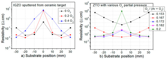
Figure 1.
Variation of the InGaZnO (IGZO) (a) and ZnSnO (ZTO) (b) resistivity as a function of the substrate position with increasing oxygen supply.
When comparing the resistivities of the IGZO and ZTO films, there is a similar effect on the lateral position. Since ZTO films were grown from metallic targets these changes are even more pronounced due to the control of oxygen amount introduced to the sputtering process in a wider range. The range of oxygen partial pressures allows for fine tuning of the thin film properties and helps to identify the role of oxygen in the deposition process.
To explain the variation of resistivity across the substrate, detailed chemical bonding states of the elements and their respective concentrations were examined by XPS. The XPS measurements, shown in Figure 2, reveal significant variations in the distribution of the elements. There is an increasing concentration of oxygen and gallium towards the center, while zinc and indium have their minimum concentrations at the center. This phenomenon is even more pronounced with oxygen addition. Moreover, the gallium peak shows a change from metallic Ga (at 17.8 eV) to ceramic Ga2O3 (at 19.8 eV) with decreasing distance from the center of the substrate (see Figure 3).
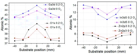
Figure 2.
Lateral distribution of elements in IGZO films.
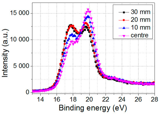
Figure 3.
X-ray photoelectron spectroscopy (XPS) of Ga 3d peak which indicates a shift from Ga2O3 (19.8 eV) at the center to metallic Ga (17.8 eV) towards the edge.
It seems that a significantly higher partial pressure is needed to oxidize the films located close to the substrate edges where not all the Ga has entered into the IGZO lattice sites but is partially segregated and has formed metallic Ga. Additionally, the chemical compositions of the films remain more or less stable at the substrate edges. However, starting at 20 mm from the substrate/target center, the concentrations of oxygen and gallium increase through the investigated volume of the material at the expense of indium and zinc. The observed lateral variations are heavily influenced by the composition and energy of the material flux towards the substrate.
From the XPS analysis together with the resistivity measurements it can be concluded that zinc and indium atoms increase the conductivity whereas gallium and oxygen atoms give rise to an increased resistivity of the sputtered IGZO films. This is seen in Figure 4.
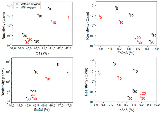
Figure 4.
IGZO films’ resistivity dependence on the element atomic concentration measured from substrate center “0” to the edges “30”.
The observed trends may be caused by oxygen vacancy variations, which determine the final free electron concentration in the sputtered films. In keeping with the study of A. Murrat [14] and G. H. Kim [15], oxygen vacancy distribution exhibits a trend with respect to Ga in InGaZnO4, since the Ga ions have a stronger chemical bond with oxygen compared to Zn and In atoms. Accordingly, we can conclude that with increasing Ga atomic content the electron concentration is suppressed and the IGZO films’ conductivity steeply decreases.
Figure 5 shows the variations in charge carrier concentration (n), Hall mobility (µ), and resistivity (ρ), of amorphous IGZO and ZTO films sputtered in an-oxygen enriched atmosphere. For the ZTO films, the resistivity steeply decreases from 105 to 10−1, whereas the carrier concentration and mobility increases with an increasing O2/Ar ratio from 0.15 to 0.18% from 1.3 × 10¹⁵ to 1.7 × 1018 cm−3 and from 2.8 to 18.2 cm2/(V·s), respectively. With a further O2/Ar ratio increase, the mobility slightly decreases, while the resistivity and carrier concentration remain stable for up to a 0.2 O2/Ar ratio. For the IGZO films, the oxygen addition slightly increases the mobility and resistivity, while the carrier concentration drops down. When comparing Hall results with XPS analysis data the effect of the Ga/Zn ratio was investigated. With an increasing Ga/Zn ratio the mobility increased from 7 to 15.6 cm2/(V·s), the resistivity increased by two orders of magnitude, and the electron concentration decreased from 4.1 × 10¹⁶ to 1.2 × 1015 cm−3.
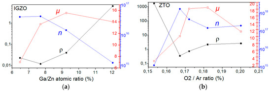
Figure 5.
Charge carrier concentration (n), Hall mobility (µ), and resistivity (ρ) of IGZO (a) and ZTO (b) films.
4. Discussion
These results illustrate the sensitivity of electrical properties to Ga impurity scattering and oxidation degree as well as to the Ga/Zn ratio in the IGZO films. For our a-IGZO films, we suggest that defects create donor levels in the band gap. The nature of these defects depends on the film composition and thus on the oxygen flow rate. Taking into account the electronic and coordination structures from Nomura et al. [3], a-IGZO is basically formed by compounds that constitute the n-type oxide semiconductors, such as In2O3, Ga2O3, and ZnO. The large spherical 5s orbitals of metals can produce extended energy states at the bottom of the conduction band, leading to more free electrons [16].
The lateral variations of the electric properties are influenced by the composition and energy of the material flux towards the substrate. As depositions are carried out on stationary substrates, variations in growth conditions across the substrate are to be expected. It is known that in magnetron sputtering of oxides, energetic negative oxygen ions may have a pronounced impact on the film properties [17]. Due to the formation of an oxide at the target surface, the partial sputtering yields of the metallic atoms change with an increasing degree of oxidation [18]. In addition, differences in the deposition rate lead to a different ratio between the metal and oxygen flux.
Our results, however, cannot be explained by either of the above effects. Instead, the results seem to indicate more efficient incorporation of oxygen and thus higher oxidation of the surface directly facing the magnetron. The observed variations can be tentatively explained by plasma activation of oxygen. The plasma density was found to be higher immediately under the target where the highest degree of oxidation also occurs. Areas outside this region required significantly higher oxygen partial pressure to reach the same degree of oxidation. The plasma activation may be very efficient in reducing the amount of unreacted oxygen in the material. This has been shown [19] to improve long-term stability of IGZO transistors.
5. Conclusions
In this work, high-mobility InGaZnO and ZnSnO films reactively sputtered at room temperature with variable oxygen addition have been presented. The effect of different plasma/discharge conditions has been examined to identify the relation between growth conditions and properties of InGaZnO and ZnSnO films. Control of oxygen incorporation and its impact on Ga and Zn atom coordination turned out to be critical for room-temperature-grown AOSs with electrical parameters suitable for thin film transistors. With an increasing Ga/Zn ratio the free electron concentration was found to drop because of a lower oxidation potential of Ga atoms compared to Zn and In ions in IGZO. The results suggest that oxygen is more efficiently incorporated into the films at the center, facing the sputtering target, in the case of IGZO and ZTO. This is somewhat surprising considering that the deposition rate is higher in the central area and it may be expected that the required oxygen pressure will be higher as well. Further studies of metal and oxygen flux across the substrate area are desirable to bring more light to the presented results.
Author Contributions
Conceptualization, T.K. and L.P.; formal analysis, L.P., P.H., A.A., and T.N.; investigation, L.P., T.K., and P.H.; resources, T.K.; writing—original draft preparation, L.P. and T.K.; writing—review and editing, P.H. and T.N.; supervision, T.K.; project administration, T.K.; funding acquisition, T.K. All authors have read and agreed to the published version of the manuscript.
Funding
This publication was supported by the project CEDAMNF, reg. No. CZ.02.1.01/0.0/0.0/15_003/0000358, co-funded by the ERDF. The authors acknowledge the support of projects CENTEM (CZ.1.05/2.1.00/03.0088) and CENTEM PLUS (LO1402).
Acknowledgments
Special thanks to the administration team of the CEDAMNF project.
Conflicts of Interest
The authors declare no conflict of interest.
References
- Fortunato, E.; Barquinha, P.; Martins, R. Oxide semiconductor thin-film transistors: A review of recent advances. Adv. Mater. 2012, 24, 2945–2986. [Google Scholar] [CrossRef] [PubMed]
- Jackson, W.B. Flexible transition metal oxide eletcronics and imprint lithography. Electron Mater. Sci. 2009, 107–142. [Google Scholar] [CrossRef]
- Nomura, K.; Ohta, H.; Takagi, A.; Kamiya, T.; Hirano, M.; Hosono, H. Room-temperature fabrication of transparent flexible thin-film transistors using amorphous oxide semiconductors. Nature 2004, 432, 488–492. [Google Scholar] [CrossRef] [PubMed]
- Hosono, H.; Nomura, K.; Ogo, Y.; Uruga, T.; Kamiya, T. Factors controlling electron transport properties in transparent amorphous oxide semiconductors. J. Non-Cryst. Solids 2008, 354, 2796–2800. [Google Scholar] [CrossRef]
- Liljeholm, L.; Junaid, M.; Kubart, T.; Birch, J.; Hultman, L.; Katardjiev, I. Synthesis and characterization of (0001)-textured wurtzite Al(1−x)BxN thin films. Surf. Coat. Technol. 2011, 206, 1033–1036. [Google Scholar] [CrossRef]
- Scragg, J.J.; Ericson, T.; Kubart, T.; Edoff, M.; Plazer-Björkmann, C. Chemical insights into the instability of Cu2ZnSnS4 films during annealing. Chem. Mater. 2011, 23, 4625–4633. [Google Scholar] [CrossRef]
- Oh, C.H.; Jang, H.; Kim, H.W.; Jung, H.; Park, H.; Cho, J.; Kim, B.S. Influence of oxygen partial pressure in In-Sn-Ga-O thin-film transistors at a low temperature. J. Alloys Compd. 2019, 805, 211–217. [Google Scholar] [CrossRef]
- Cai, M.X.; Yao, R.H. A drain current model for amorphous InGaZnO thin film transistors considering temperature effect. Solid State Electron. 2018, 141, 23–30. [Google Scholar] [CrossRef]
- Gao, X.; Andersson, J.; Kubart, T.; Nyberg, T.; Smith, U.; Lu, J.; Hultman, L.; Kellock, A.J.; Zhang, Z.; Lavoie, C.; et al. Emitaxy of ultrathin NiSi2 films with predetermined thickness. Electrochem. Solid-State Lett. 2011, 14, H268–H270. [Google Scholar] [CrossRef]
- Kubart, T.; Nyberg, T.; Berg, S. Modelling of low energy ion sputtering from oxide surfaces. J. Phys. D Appl. Phys. 2010, 43, 205204. [Google Scholar] [CrossRef]
- Aiempanakit, M.; Kubart, T.; Larsson, P.; Sarakinos, K.; Jensen, J.; Helmersson, U. Hysteresis and process stability in reactive high power impulse magnetron sputtering of metal oxides. Thin Solid Films 2011, 519, 7779–7784. [Google Scholar] [CrossRef]
- Prusakova, L.; Novak, P.; Kulha, P.; Ocenasek, J.; Savkova, J.; Pastorek, L.; Sutta, P. Modeling and fabrication of single cantilever piezoelectric microgenerator with optimized ZnO active layer. Thin Solid Films 2015, 591, 305–310. [Google Scholar] [CrossRef]
- Xiao, P.; Huang, J.; Dong, T.; Yuan, J.; Yan, D.; Xie, J.; Tan, H. X-ray photoelectron spectroscopy analysis of the effect of photoresist passivation on InGaZnO thin-film transistors. Appl. Surf. Sci. 2019, 471, 403–407. [Google Scholar] [CrossRef]
- Murat, A.; Medvedeva, J.E. Composition-dependent oxygen vacancy formation in multicomponent wide-band-gap oxides. Phys. Rev. B 2012, 86, 085123. [Google Scholar] [CrossRef]
- Kim, G.H.; Jeong, W.H.; Kim, H.J. Electrical characteristics of solution-processed InGaZnO thin film transistors depending on Ga concentration. Phys. Status Solidi A 2010, 207, 1677–1679. [Google Scholar] [CrossRef]
- Martin, N.; Nyberg, T.; Kapaklis, V. Low temperature electronic transport in sputter deposited a-IGZO films. Curr. Appl. Phys. 2014, 14, 1481–1485. [Google Scholar] [CrossRef]
- Welzel, T.; Ellmer, K. Negative oxygen ion formation in reactive magnetron sputtering processes for transparent conductive oxides. J. Vac. Sci. Technol. A 2012, 30, 061306. [Google Scholar] [CrossRef]
- Kubart, T.; Nyberg, T.; Pflug, A.; Siemers, M.; Austgen, M.; Koehl, D.; Wuttig, M.; Berg, S. Modelling of sputtering yield amplification effect in reactive deposition of oxides. Surf. Coat. Technol. 2010, 204, 3882–3886. [Google Scholar] [CrossRef]
- Hosono, H. Ionic amorphous oxide semiconductors: Material design, carrier transport, and device application. J. Non-Cryst. Solids 2006, 352, 851–858. [Google Scholar] [CrossRef]
© 2019 by the authors. Licensee MDPI, Basel, Switzerland. This article is an open access article distributed under the terms and conditions of the Creative Commons Attribution (CC BY) license (http://creativecommons.org/licenses/by/4.0/).