Article

AC and Phase Sensing of Nanowires for Biosensing

1
Department of Electrical, Electronic and Information Engineering, University of Bologna, Cesena Campus, Cesena 47521, Italy
2
School of Electronics and Computer Sciences, and the Institute for Life Sciences, University of Southampton, Southampton SO17 1BJ, UK
*
Author to whom correspondence should be addressed.
Biosensors 2016, 6(2), 15; https://doi.org/10.3390/bios6020015
Submission received: 28 January 2016 / Revised: 6 April 2016 / Accepted: 9 April 2016 / Published: 19 April 2016
(This article belongs to the Special Issue Micro- and Nano-Bio-Interfaces)

Abstract

:
Silicon nanowires are label-free sensors that allow real-time measurements. They are economical and pave the road for point-of-care applications but require complex readout and skilled personnel. We propose a new model and technique for sensing nanowire sensors using alternating currents (AC) to capture both magnitude and phase information from the sensor. This approach combines the advantages of complex impedance spectroscopy with the noise reduction performances of lock-in techniques. Experimental results show how modifications of the sensors with different surface chemistries lead to the same direct-current (DC) response but can be discerned using the AC approach.

1. Introduction

The development of sensitive and specific biosensors remains a significant challenge. Among many issues, one major problem is the miniaturization and efficiency of the readout electronics. Silicon nanowires (Si-NWs) and nanoribbons have been proposed as for a new class of biosensors, primarily because they are label-free sensors and allow real time measurements [1,2,3], even in complex physiological media [4,5,6].
Nanowire sensors are very low cost (disposable) sensors since fabrication can be performed using standard top-down processes, based on mature photolithography, thin film deposition and plasma etching [7,8,9,10]. However, a typical readout system is bulky and expensive requiring a complex setup and skilled personnel. To enable the routine use of biochemical sensors, they will have to be simple and low cost, so that they can be used in point-of-care locations other than clinical laboratories. To address this need, integrated sensor systems are emerging that can be used within portable systems [11,12], [13,14,15] where the sensor chips are fused with custom electronics into a user-friendly package.
Nanowire and nanoribbon sensing is usually performed with simple DC measurements [16,17,18,19] although alternating currents (AC) characterization of the electrical properties of nanowires (NWs) is a standard procedure [20,21,22]. In the last few years, nanowire AC sensing has become an important technique which has advantages with respect to DC sensing [23]. However, the majority of the literature describes AC sensing based on single-phase lock-in detection, where only the magnitude of the impedance, or power response of the NW (or carbon nanotube), is investigated [24,25,26]. Only a few recent manuscripts describe NW complex AC sensing, measuring the analyte with both magnitude and phase of the impedance [27,28].
In this paper, we investigate the potential of complex AC sensing of Si-NWs to provide information on magnitude and phase of the impedance. Since the exact response of the nanowire sensors is not fully understood, it is possible that measurement of the complex NW impedance could provide more information on the binding events occurring at the interface, including time-dependent behavior of local charges. DC sensing of NWs is based on modulation of the channel resistivity due to changes in the surface potential. Nanowires can also be viewed as a distributed line with the resistance and capacitance per unit length determined by the concentration of target molecules. In particular, NW capacitance could reveal further information concerning the target molecules, which could only be sensed by AC methods since AC methods are sensitive to the displacement of charge at the interface. Therefore, the development of a compact and precise readout system capable of measuring the complex AC impedance of nanowires is an important step for testing the dynamic properties of these nanosensors.
This paper describes an AC sensing system based on a dual-phase lock-in technique. Impedance spectrometry is used to measure NW characteristics. Results reveal how changing the surface charge on the nanowire leads to the same DC response but different AC impedance properties. Section 2 provides a full description of the entire setup, from fabrication and physical behavior of nanowires to implementation of electronic circuits and microfluidic of the AC sensing system. This section also provides the motivation to the AC approach. Finally, Section 3 describes a simple electrical model for the NW and compares it with experimental DC and AC measurements.

2. Materials and Methods

2.1. Device Under Test

The silicon nanowire chips (14.8 × 14.8 mm2) contain 8 sets of p-type top-down fabricated nanowires [7]. The devices were fabricated using a low-cost photolithography process, based on thin film technology and a dry spacer etching technique. Such devices are suitable for low cost mass production.
The nanowires are 40 µm long with a rectangular cross section of 100 nm × 100 nm. They are arranged in sets. The outer four sets have the same number of parallel nanowires (30); while the inner sets have a variable number of parallel nanowires (10 to 320), see Figure 1a.
Figure 1a shows the device cross section. It consists of an n-type silicon substrate, 750 nm plasma enhanced chemical vapor deposited (PECVD) oxide layer, and a 300 nm silicon nitride layer. Oxide pillars are created by PECVD and patterned using photolithography and anisotropic etching. On those pillars a 100 nm amorphous silicon (α-Si) film is deposited by low-pressure chemical vapor deposition (LPCVD) at 560 °C and then doped by boron implantation at a dose of 1 × 10¹⁸/cm2 and an energy of 25 keV. Rectangular-shaped nanowires are formed using a special anisotropic dry-etching process performed using an Oxford Instruments Plasma Technology 80+ reactive ion etcher (RIE) system at 160 W input power, with a SF6 flow of 12 sccm, an O2 flow of 12 sccm and a pressure of 30 mTorr.
At the end of the process, a gate oxide, nominally 10 nm thick, is grown at 900 °C creating a stable surface for nanowire sensing in liquid. Finally, aluminum contacts were made at both end of the polysilicon nanowire by the creation of heavily doped (with a dose of 1 × 10²¹/cm2) source/drain pad regions, highlighted in red in Figure 1b. The sensing window (green in Figure 2b) over the nanowire is the only exposed region, while the rest of the NW is covered with layer of photoresist.
Metal pads close to the lower scribe lines (Figure 1a) provide contacts and have a pitch of 1 mm, compatible with standard commercial connectors (Samtec SEI series). This simplified connection to a PCB allowing different NW chips to be tested.

2.2. NW Physical Model

A silicon NW senses molecules based on modulation of its conductance by a change in the charge density at the interface, similarly to an ion-sensitive field effect transistor (ISFET). The gate-sensing layer separates the nanowire oxide from the aqueous electrolyte [29,30,31].
Any free charge in the system, electrons/holes in semiconductors and ions in solution, are subject to the same laws: Electrostatic forces and the statistical distribution of charges. Therefore the charge distribution can be determined from the electrostatic potential profile given by Poisson’s equation, and the distribution of charges given by Boltzmann statistics.
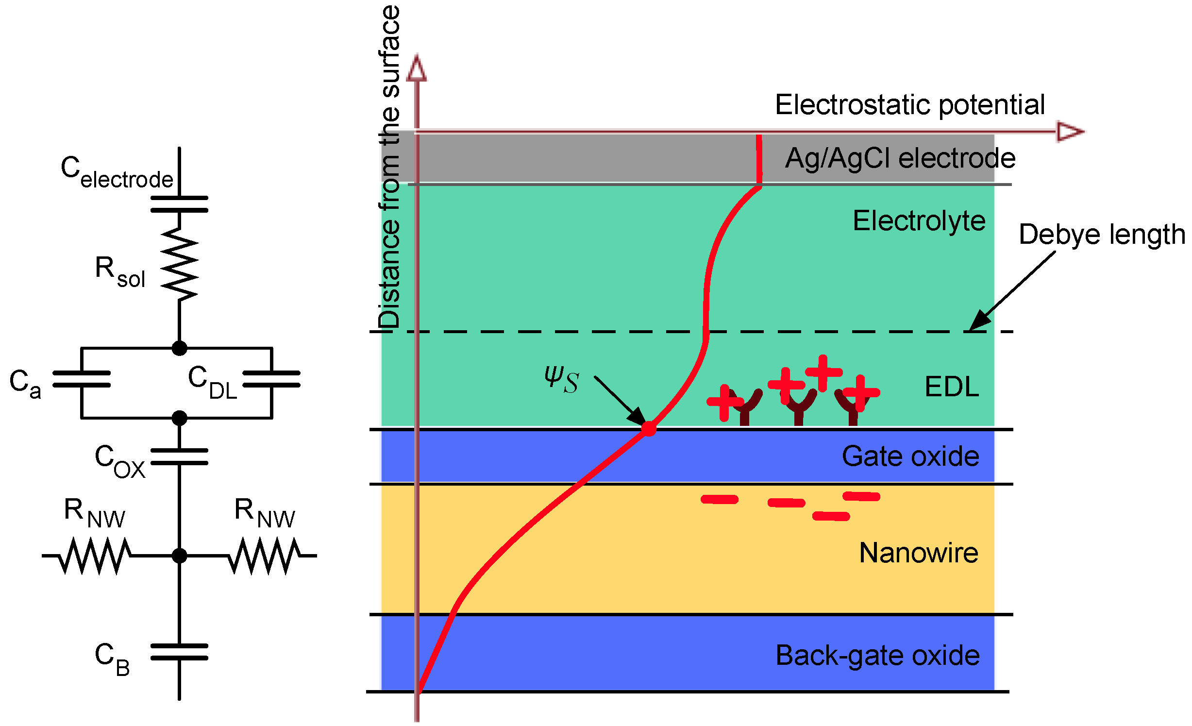
Assuming a vertical cross section divided into electrically independent parts (electrolyte, gate oxide and semiconductor), the free carriers in each section have a non-uniform distribution given by a solution to the Poisson-Boltzmann equation. The solution to this non-linear equation gives the exact profile of the potential: for example in the electrolyte the potential decays exponentially from the surface. This behavior is called electrical double layer (EDL) and the decay distance is the Debye length λD [32]. The differential capacitance per unit area of the double layer is:
C D L = d σ d ψ S ε 0 ε r λ D
where σ is the surface charge density, and ψS is the electrostatic potential at the interface. The Debye length is given by:
λ D = ε 0 ε r k T 2 z 2 q 2 n 0
where z is the ionic valance and n0 is the ion concentration in the bulk. The charge density of the semiconductor, and thus the conductance of the NW, is non-linearly related to the electrostatic potential ψS at the interface as shown in [33] (Figure 2). The Poisson-Boltzmann model does not take into account the contribution of the charge equilibrium at the oxide-electrolyte interface. This effect, when added to the model, is called the site-binding model [33], where typically binding occurs at a range shorter than the Debye length. More specifically, the surface of any oxide consists of hydroxyl groups (silanol groups Si-OH for silicon dioxide) that may be protonated or deprotonated depending on the pH of the solution and on the isoelectric point (IEP) of the surface, resulting in a positively or negatively charged surface according to:
S i O H 2 + S i O H + H + S i O H S i O + H +
If the pH of the solution is higher than the IEP then the surface is deprotonated and acts as if negative charges have been added to the surface, increasing the concentration of the holes and therefore the nanowire conductance. The opposite occurs if the pH is lower than the IEP.
From the viewpoint of this model, the equilibrium constants need to be included to complete the description with respect to H+ concentration. The model is equivalent to that derived for ISFETs by Bergveld in 1970 [34]. A detailed description of the site-binding model is found in [35]. Cui et al. showed how nanowires can be highly sensitive pH sensors [36,37].
On the base of the above we expect the following:
  • The concentration of the solution modulates the Debye length according to Equation (2), thus changing the exponential decay of the electrostatic potential (Figure 2, right), modeled as the double layer capacitance CDL.
  • Any charge variation due to site-binding (such as pH and molecular interactions at the interface) occurring within the Debye length directly influence the potential profile at the interface according to Poisson’s equation. The concentration of hydrogen ions is usually much smaller than the concentration of salt ions; therefore these play a negligible role in determining the Debye length.
  • The functionalization of the NW surface induces, together with local electrostatic potential variation, charge dynamic effects that can be modeled as a differential capacitance CA in parallel with the double layer capacitance [33].
An electrical model of the NW interface together with a cross-section is illustrated in Figure 2. The distributed model that will be shown in Section 3 is based on the above model. In terms of sensing, DC measurements can measure variations in RNW (mainly related to site-binding effects), whilst AC sensing can measure, in addition to RNW, CDL and CA, giving a deeper understanding of the physical phenomenon acting on the surface, hence a different sensing mechanism.

2.3. AC Nanowire Sensing

The impedance of nanowires depends on time-dependent variations in the electrical potential, as given by equation (1) and/or by changes in bound charges.
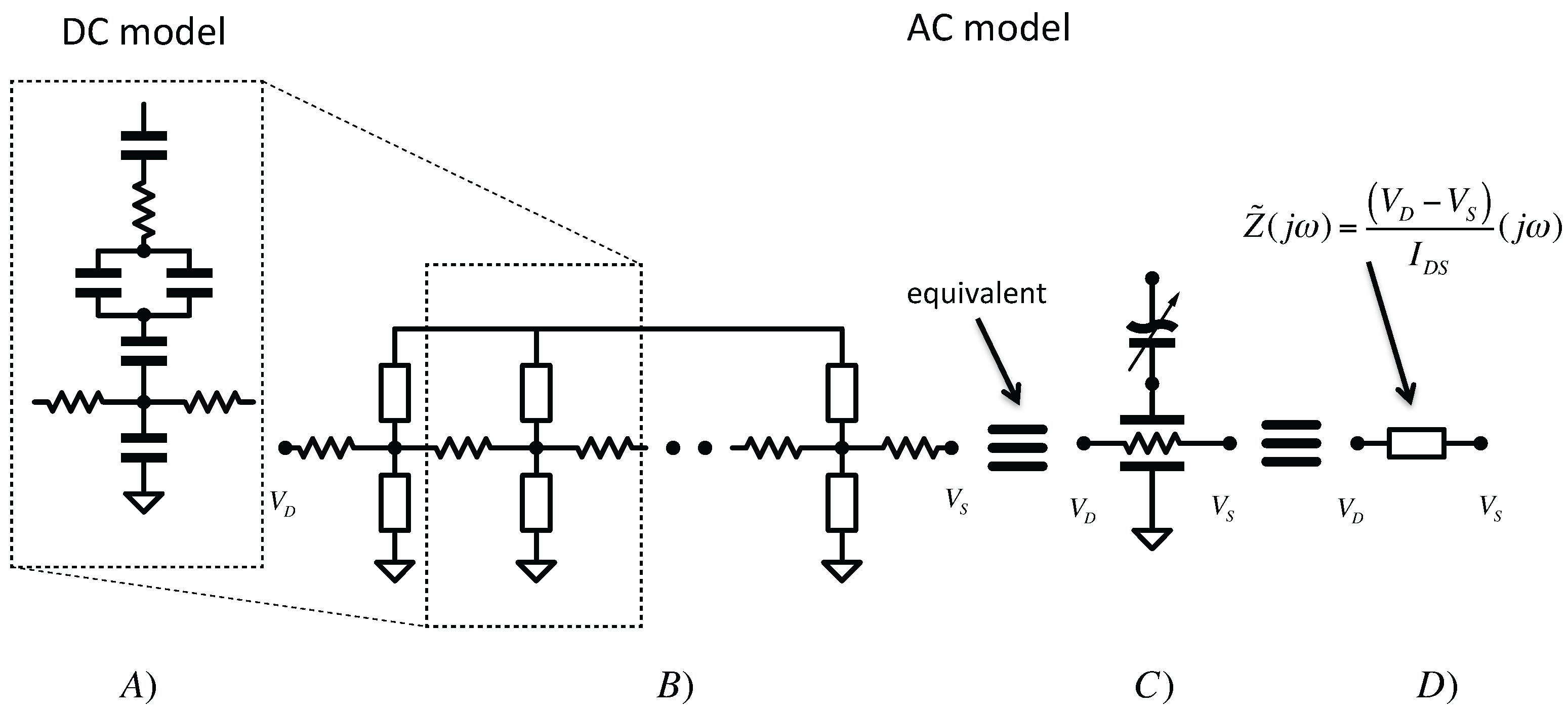
On the basis of the DC-sensing simplified model reported in Figure 2, the AC sensing could be defined by an infinite number of DC-sensing stages (Figure 3A) placed side-by-side as illustrated in Figure 3B describing a distributed element model shown in Figure 3C. Therefore, our approach is sensing the equivalent impedance illustrated in Figure 3D. The accuracy of this model using SPICE simulations with respect to experimental results will be shown in the next section.
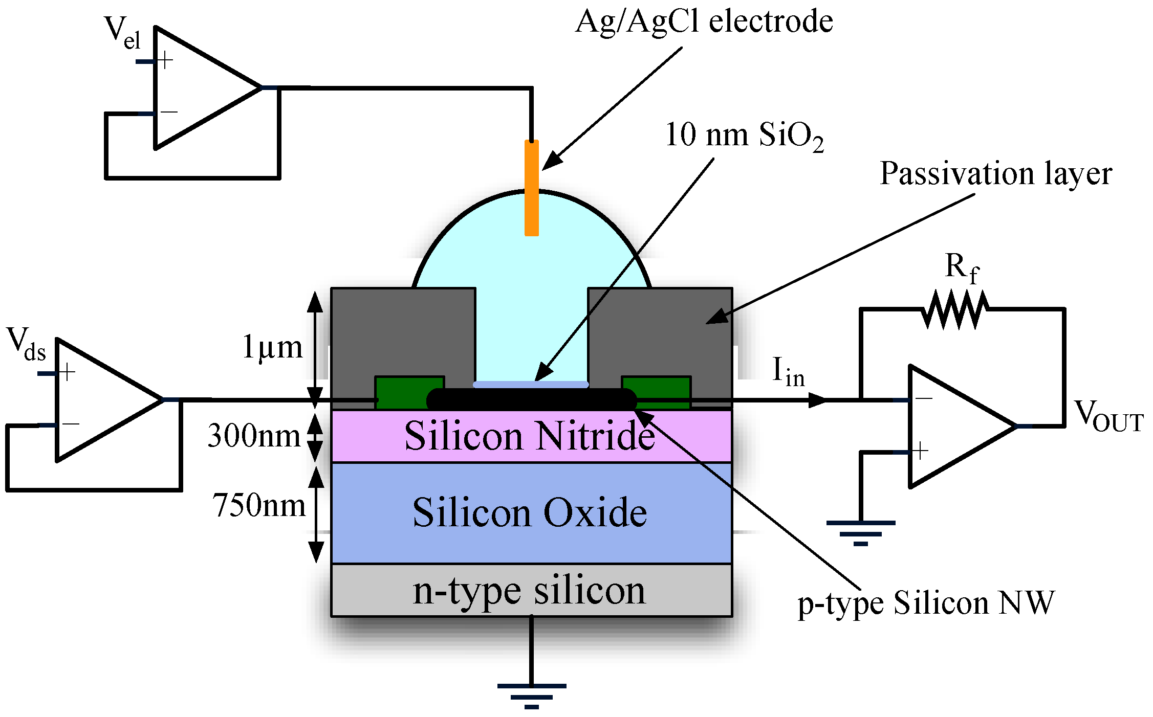
There are different ways of applying AC signals across a nanowire and a typical single-ended architecture is shown in Figure 4. The exact way in which the AC signal is applied depends on the static characteristic of the device. The use of small Vgs or Vds signal is interchangeable and depends on the chosen bias conditions. First, we characterized the nanowire in the Id(Vds, Vgs) plane, noting that for small Vgs (i.e., Vgs ≤ 100 mV) the device works in a strong inversion, linear region. Therefore, for this bias condition, the sensitivity of the drain current to Vds changes is stronger than for changes in Vgs. Therefore, it is preferable to apply the signal to the source/drain terminal with the bulk set to ground. This approach is preferable for impedimetric sensing since the voltage and the current are applied to the same terminal, thus avoiding phase error. A small sinusoidal voltage (100 mV) is applied to one end of the nanowire while a current is measured at the other. The same scheme could be used for DC mode simply using an offset bias on one side of the NW.

2.4. Impedance Lock-In Principle

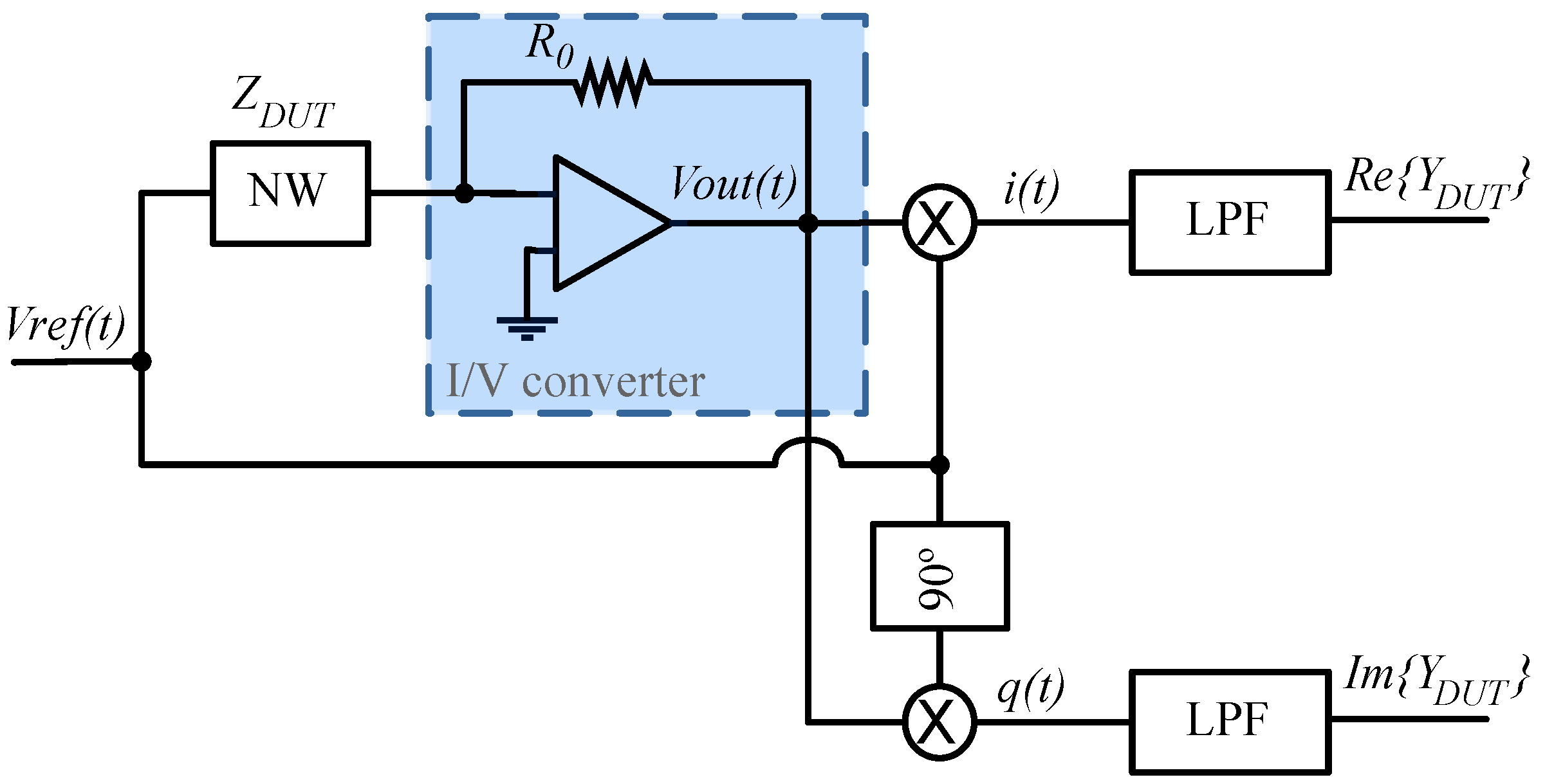
The dual-phase lock-in is a phase sensitive detector that measures amplitude and phase of an AC signal in a noisy environment. The operating principle is depicted in Figure 5. A sinusoidal stimulus:
V r e f ( t ) = V 0 cos ( ω 0 t )
is applied to a device under test (DUT) and the current is converted into an output voltage:
V o u t ( t ) = V r e f Z D U T R 0 = V 0 | Z D U T | R 0 cos ( ω 0 t θ D U T )
where R0 is the transresistance of the I/V converter, ZDUT is the complex DUT impedance and θDUT is the phase contribution of ZDUT.
Both voltages, VOUT and VREF, are fed into a phase-sensitive detector where VOUT is multiplied by the reference voltage and the 90° shifted version, providing an in-phase signal i and quadrature signal q as follows:
i = V O U T ( t ) V 0 cos ( ω 0 t ) = V 0 2 | Z D U T | R 0 cos ( ω 0 t θ D U T ) cos ( ω 0 t ) = V 0 2 2 | Z D U T | R 0 [ cos ( θ D U T ) + cos ( 2 ω 0 t θ D U T ) ]
q = V O U T ( t ) V 0 sin ( ω 0 t ) = V 0 2 | Z D U T | R 0 cos ( ω 0 t θ D U T ) sin ( ω 0 t ) = V 0 2 2 | Z D U T | R 0 [ sin ( 2 ω 0 t θ D U T ) sin ( θ D U T ) ]
Low-pass filters remove the high frequency terms in Equations (6) and (7), giving the real and imaginary parts of the DUT admittance:
e { Y D U T } ~ R 0 V 0 2 2 | Y D U T | cos ( θ D U T )
m { Y D U T } ~ R 0 V 0 2 2 | Y D U T | sin ( θ D U T )

2.5. Circuit Implementation

Typical nanowire resistance is in the range of 100 kΩ to 100 MΩ [5,6,8,19,38,39,40] so that the currents are of the order of tens to hundreds of nA. Our measurement system is a portable test board that implements a two electrode potentiostat with a lock-in measurement technique for complex impedance detection as described in previous section [41].
The board is based on the AD630 switched demodulator [42]. A transimpedance input amplifier converts the current signal from the sensors prior to the phase-sensitive detection. The signal is pre-amplified by an AD822 which shows low-power consumption, rail-to-rail, low noise operating performance (13 nV/√Hz @ 10 kHz), and low input bias current [43].
The signal conditioning process is shown in Figure 6, and has 3 stages: First two stages consist of a finite impulse response digital low-pass filters using a FIR Kaiser window and a decimator. Weight taps were calculated with MATLAB to provide the best configuration for all the required frequencies.
Filtering and data manipulation are performed in the digital domain, providing a particularly flexible system, with a simple analog front-end that can be used for different applications. An auxiliary potential control circuit applies a back-gate and/or liquid gate potential.

2.6. Microfluidics

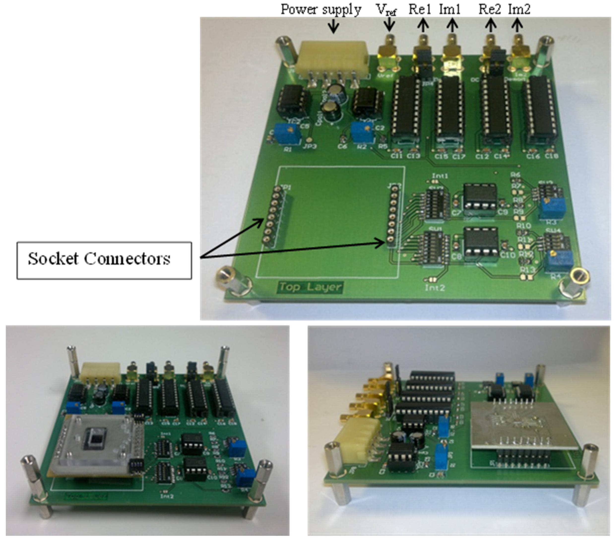
The board is designed to be modular and has a single electronic readout interface. Different sensors can be connected using a socket (Figure 7). A custom microfluidic board (4 × 4 cm2) interfaces to the nanowire chip [7]. The microfluidic interface consists of four parts (Figure 8):
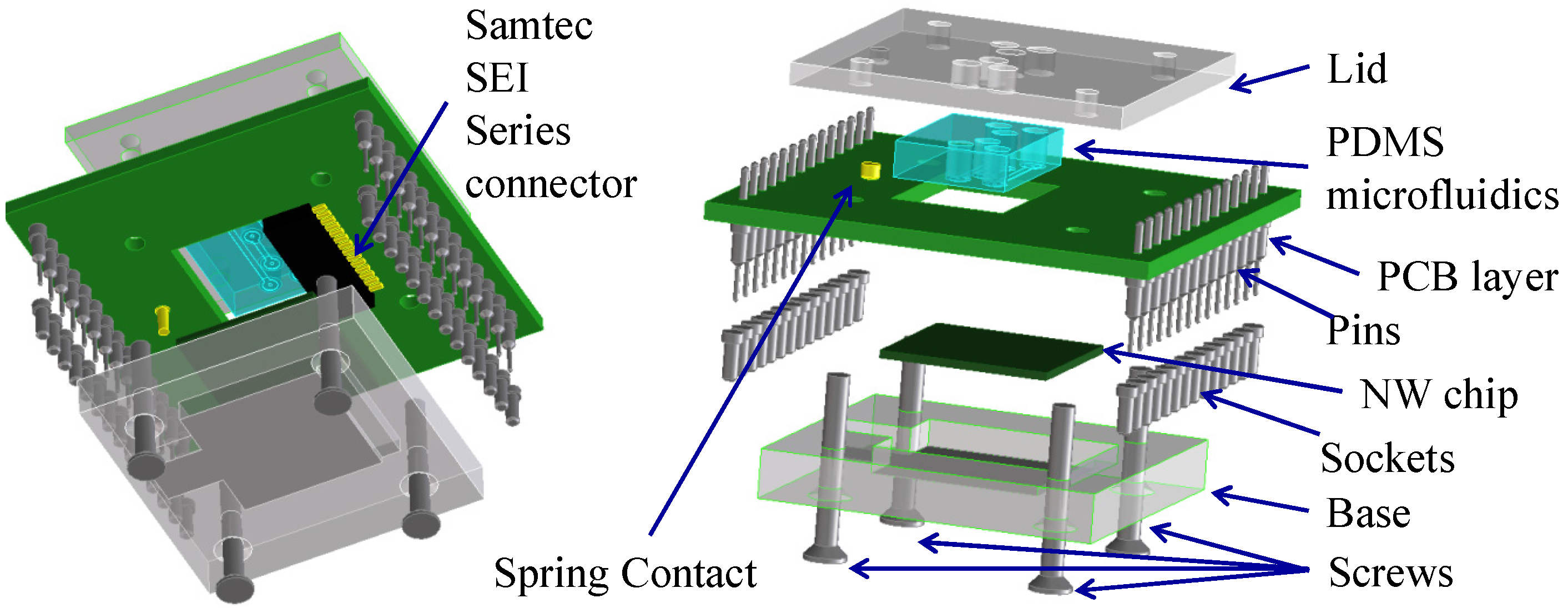
  • A base, which holds the NW chip and makes contact to the back gate with a small piece of aluminium foil providing. A recess enables automatic alignment of the contact pads of the NW chip with the connector.
  • A windowed two-layer PCB, with Samtec® SEI connector, a spring connector and two 4-way surface mount device (SMD) switches. The spring connector contacts the aluminium foil base. The 4-way SMD switches connect the VREF signal to the selected Si-NWs under test.
  • A rectangular PDMS microfluidics gasket, designed and moulded as required (e.g., with or without microchannels for solution flow), ensures a tight seal between the sensitive NW chip surface and the bottom layer of the PCB avoiding electrolyte leakage;
  • A lid to package the microfluidic gasket as well as the whole device.

3. Results and Discussion

3.1. Equivalent Model

In order to understand the complex impedance behavior of the device, an electrical model of the nanowire is proposed in Figure 9. This is a distributed network composed of a series of identical RCR T-network elements surrounded by lumped parasitic capacitances. The AC excitation consists in applying a sinusoidal voltage (100 mV) across the NW and thus measuring the corresponding device current. However, the device is characterized by a distributed RC time constant, as shown in Figure 9A, given by the channel resistance RNW and channel capacitances. On the solution side we have the double layer capacitance CDL and the thin oxide capacitance COX, whilst on the other side we have the bulk capacitance CB. Since the excitation frequency is comparable to the reciprocal of the time constant, we cannot model the device with a lumped RC circuit. Therefore, in our approach we model the device with a distributed circuit (50 sections) as sown in Figure 9A. The model has been simulated with SPICE in order to determine the relationship between the amplitude and the current that is described by the complex impedance Z ˜ ( j ω ) and compare it with the experimental results. The whole device is shown in Figure 9B.
To setup the model, the parasitic capacitance of the contacts was measured for several different nanowire chips using a probe station (Cascade Microtech prober, associated with Agilent 4279A 1 MHz CV meter) both in air and buffer conditions. Values range from 2 to 5 pF for the track-track capacitance (CL) and from 18 to 30 pF for the track-bulk capacitance (Cstray).
Assuming the NW works in the strong inversion regime, it can be modeled as a variable resistor modulated by surface charges neglecting the semiconductor depletion capacitance, usually taken into account in modelling FET devices [2], so that the only variable is the capacitive contribution from the semiconductor interface (CS) [14]. This surface capacitance CS is the series combination of the oxide capacitance COX, (the SiO2 layer on top of the NW), and the electrical double layer capacitance CDL as illustrated in Figure 9A. When the surface oxide is changed by chemical modification, an additional capacitance CA is added in parallel with CDL in the model, as explained in [32]. Value of COX has been calculated from geometry and physical parameters, while CDL was estimated from experimental data.
The charge transfer resistance usually considered in electrode-electrolyte interface model [15,16] can be neglected in the absence of Faradaic reactions. This is confirmed by measurements of the current between the liquid gate electrode and the nanowire drain contact, which is <10 pA. The impedance of the electrode/electrolyte interface [31,32] at the liquid gate electrode was also neglected due to its very large dimension compared to the nanowires. It is modeled as an ideal electrode and sets the potential of the buffer solution.
Complex impedance measurements of bare nanowires immersed in pH 7 phosphate buffer were fitted to this circuit. As shown in Figure 9C,D, the equivalent model matches the data with the following parameters: RNW = 3 MΩ, CS = COX//CDL = 7.5 pF, CDL = 74 pF, CL = 5 pF, CB = 100 pF, Cstray = 30 pF, RSOL = 2 MΩ. Note that according to the graphs, the AC magnitude sensing follows the DC behavior at low frequency whilst at higher frequency it is attenuated by a factor depending on the frequency, as in a dominant pole behavior. Note also in Figure 9D that, as long as the frequency is very low, the voltage and the current are in-phase as in a pure resistor, whilst for high frequency the voltage and the current are in quadrature phase-lag, as expected.

3.2. AC Measurements

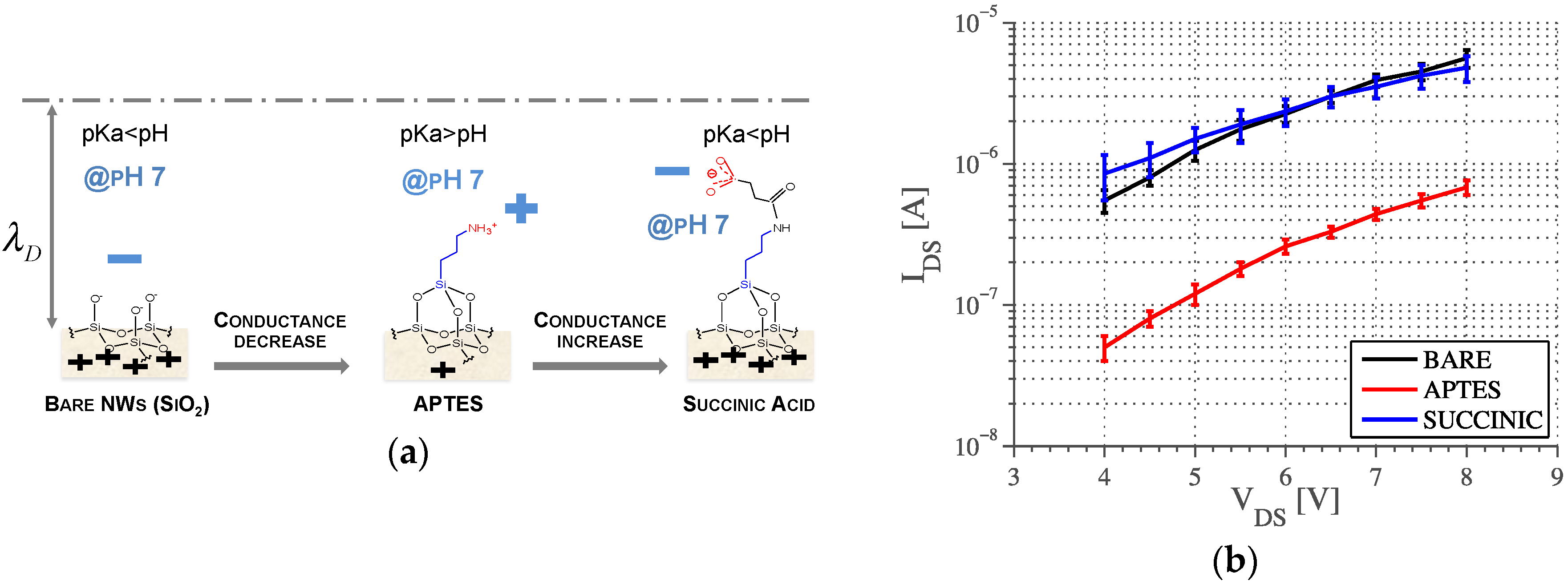
The surface of the nanowires were modified using two different chemistries: (i) vapor deposition of 3-aminopropyltri-ethoxysilane (APTES); and (ii) further exposure to N-(3-Dimethylaminopropyl)-N′-ethylcarbodiimide hydrochloride, N-hydroxysulfosuccinimide sodium salt and succinic acid. These two methods produce surfaces with different surface charge and dissociation constants (pKa) as confirmed by DC measurements at fixed pH 7. The nanowire conductivity decreases after APTES functionalization due to the presence of the amino group (pKa~9) that protonates at pH 7, reducing the local concentration of holes (carriers) in the p-type nanowire [26]. Conversely, it increases with the succinic acid, since the terminal carboxyl group (pKa~5) deprotonates at pH 7, resulting in a conductance similar to the bare nanowires, as previously reported [7] (Figure 10). The DC results presented in Figure 10b show how the behavior of the bare and succinic functionalized wires are similar.
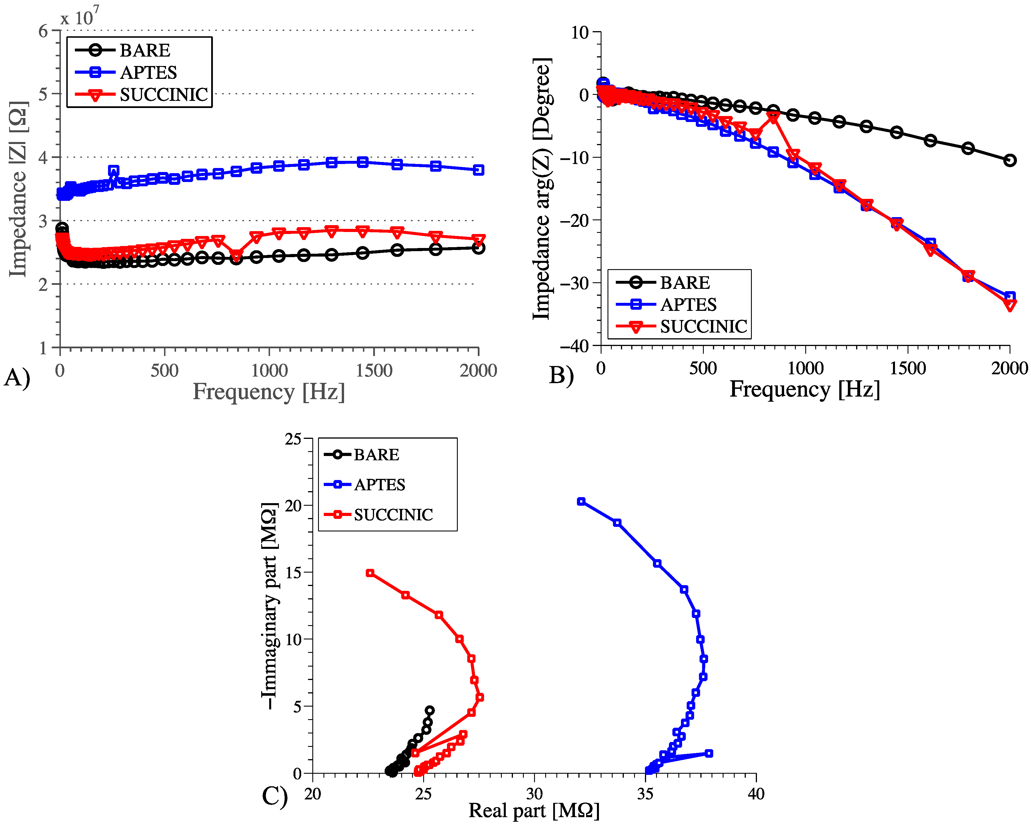
These DC results were confirmed using AC sweeps of nanowires immersed in 1 mM phosphate buffer solution at pH 7 (Figure 11). For these experiments the custom acquisition board was used, as described in section II. This board can work up to 2 kHz; which is low enough to observe all the dynamics involved in NW sensing, and high enough to demonstrate AC phase sensing. The impedance magnitude is in agreement with the DC measurements confirming the expected behavior of the modulation of conductivity in response to changes in surface charge. The phase plot shows that the APTES and succinic acid nanowires have similar properties, but different to bare nanowires. This could be explained by a variation in the site-binding capacitance CA. We summarize the behavior as follows:
  • The effect of the charge change following functionalization changes the NW resistance, thus the magnitude of the AC impedance is similar to the DC (bare NW and succinic acid showed the same behavior);
  • Surface chemistries with similar effects on NW charge have different properties that can be measured by phase detection and modeled through different values of CA, which should be added in parallel with CDL in the model, as explained in [32].
The behavior can also be represented with a Cole-Cole plot shown in Figure 11C. The bare and succinic response have the same magnitude and the same intercept at f = 0 Hz (as in DC) whilst APTES has larger magnitude values. On the contrary, succinic and APTES have the same phase behavior whilst bare NWs show a much smaller phase shift.

4. Conclusions

Nanowire and nanoribbon sensing is usually performed with either quasi-static measurements (DC) or single-phase lock-in. Those only probe changes in the surface charge on the NW conductance. In this paper we introduce AC phase sensing of nanowires. A compact AC impedance system was developed based on a lock-in technique. pH measurements of different nanowires were used to compare AC sensing against standard DC sensing. The system demonstrates the ability of AC sensing to discriminate between different surface chemistries that are indistinguishable by DC measurement. An equivalent electrical circuit of the nanowire has been proposed to model the complex impedance of the nanowire device.

Acknowledgments

This work was funded by the Engineering and Physical Sciences Research Council (UK) through grant EP/H044795/1 and by EU and National funds (IT) under the ENIAC-JTI project LAB4MEMs. The data for this paper can be obtained from University of Southampton e-prints repository on http://dx.doi.org/10.5258/SOTON/394688.

Author Contributions

Marco Crescentini wrote the paper and analyzed the data contributing to the setup of the architecture and of the approach. Michele Rossi implemented the electronics and microfluidics platform, and performed the experiments. Marco Tartagni contributed to the data analysis, and theoretical framework of electronic sensing. Peter Ashburn, Marta Lombardini contributed to the design and fabrication of the nanowires together with Hywel Morgan that also gave insights into the physics of nanowires in electrolytes. Enrico Sangiorgi contributed to device modeling insights understanding.

Conflicts of Interest

The authors declare no conflict of interest. The founding sponsors had no role in the design of the study; in the collection, analyses, or interpretation of data; in the writing of the manuscript, and in the decision to publish the results.

Abbreviations

The following abbreviations are used in this manuscript:
ACAlternating Current
DCDirect Current
NWNanowire
CMOSComplementary Metal Oxide Semiconductor
Si-NWSilicon Nanowire
PECVDPlasma Enhanced Chemical Vapor Deposited
LPCVDLow-Pressure Chemical Vapor Deposition
RIEReactive Ion Etcher
PCBPrinted Circuit Board
ISFETIon-Sensitive Field Effect Transistor
EDLElectrical Double Layer
IEPIsoelectric Point
DUTDevice Under Test
SMDSurface Mount Device
PDMSPolydimethylsiloxane
APTES3-aminopropyltri-ethoxysilane

References

  1. Ramgir, N.S.; Yang, Y.; Zacharias, M. Nanowire-based sensors. Small 2010, 6, 1705–1722. [Google Scholar] [CrossRef] [PubMed]
  2. Chen, K.-I.; Li, B.-R.; Chen, Y.-T. Silicon nanowire field-effect transistor-based biosensors for biomedical diagnosis and cellular recording investigation. Nano Today 2011, 6, 131–154. [Google Scholar] [CrossRef]
  3. Curreli, M.; Zhang, R.; Ishikawa, F.N.; Chang, H.-K.; Cote, R.J.; Zhou, C.; Thompson, M.E. Real-time, label-free detection of biological entities using nanowire-based FETs. IEEE Trans. Nanotechnol. 2008, 7, 651–667. [Google Scholar] [CrossRef]
  4. Stern, E.; Vacic, A.; Rajan, N.K.; Criscione, J.M.; Park, J.; Ilic, B.R.; Mooney, D.J.; Reed, M.A.; Fahmy, T.M. Label-free biomarker detection from whole blood. Nat. Nanotechnol. 2010, 5, 138–142. [Google Scholar] [CrossRef] [PubMed]
  5. Zhang, G.; Chai, K.T.C.; Luo, H.Z.H.; Huang, J.M.; Tay, I.G.K.; Lim, A.E.; Je, M. Multiplexed detection of cardiac biomarkers in serum with nanowire arrays using readout ASIC. Biosens. Bioelectron. 2012, 35, 218–223. [Google Scholar] [CrossRef] [PubMed]
  6. Krivitsky, V.; Hsiung, L.-C.; Lichtenstein, A.; Brudnik, B.; Kantaev, R.; Elnathan, R.; Pevzner, A.; Khatchtourints, A.; Patolsky, F. Si nanowires forest-based on-chip biomolecular filtering, separation and preconcentration devices: Nanowires do it all. Nano Lett. 2012, 12, 4748–4756. [Google Scholar] [CrossRef] [PubMed]
  7. Hakim, M.M.A.; Lombardini, M.; Sun, K.; Giustiniano, F.; Roach, P.L.; Davies, D.E.; Howarth, P.H.; de Planque, M.R.R.; Morgan, H.; Ashburn, P. Thin film polycrystalline silicon nanowire biosensors. Nano Lett. 2012, 12, 1868–1872. [Google Scholar] [CrossRef] [PubMed]
  8. Chen, S.; Bomer, J.G.; van der Wiel, W.G.; Carlen, E.T.; van den Berg, A. Top-down fabrication of sub-30 nm monocrystalline silicon nanowires using conventional microfabrication. ACS Nano 2009, 3, 3485–3492. [Google Scholar] [CrossRef] [PubMed]
  9. Zeimpekis, I.; Sun, K.; Hu, C.; Thomas, O.; de Planque, M.R.; Chong, H.M.; Morgan, H.; Ashburn, P. Study of parasitic resistance effects in nanowire and nanoribbon biosensors. Nanoscale Res. Lett. 2015, 10. [Google Scholar] [CrossRef] [PubMed]
  10. Accastelli, E.; Scarbolo, P.; Ernst, T.; Palestri, P.; Selmi, L.; Guiducci, C. Multi-wire tri-gate silicon nanowires reaching milli-pH unit resolution in one micron square footprint. Biosensors 2016, 6. [Google Scholar] [CrossRef] [PubMed] [Green Version]
  11. Manickam, A.; Johnson, C.A.; Kavusi, S.; Hassibi, A. Interface design for CMOS-integrated Electrochemical Impedance Spectroscopy (EIS) biosensors. Sensors 2012, 12, 14467–14488. [Google Scholar] [CrossRef] [PubMed]
  12. Xu, J.; Offermans, P.; Meynants, G.; Tong, H.D.; van Rijn, C.J.M.; Merken, P. A low-power readout circuit for nanowire based hydrogen sensor. Microelectron. J. 2010, 41, 733–739. [Google Scholar] [CrossRef]
  13. Offermans, P.; Tong, H.D.; van Rijn, C.J.M.; Merken, P.; Brongersma, S.H.; Crego-Calama, M. Ultralow-power hydrogen sensing with single palladium nanowires. Appl. Phys. Lett. 2009, 94. [Google Scholar] [CrossRef]
  14. Van den Brink, F.T.G.; Gool, E.; Frimat, J.-P.; Bomer, J.; van den Berg, A.; Le Gac, S. Parallel single-cell analysis microfluidic platform. Electrophoresis 2011, 32, 3094–3100. [Google Scholar] [CrossRef] [PubMed]
  15. Zagnoni, M. Miniaturised technologies for the development of artificial lipid bilayer systems. Lab Chip 2012, 12, 1026–1039. [Google Scholar] [CrossRef] [PubMed]
  16. Carlen, E.T.; van den Berg, A. Labs-on-a-chip and nanosensors for medical applications and life sciences. In Proceeding of the 2013 IEEE International Electron Devices Meeting, Washington, DC, USA, 9–11 December 2013.
  17. Zaborowski, M.; Dumania, P.; Tomaszewski, D.; Czupryniak, J.; Kokot, M.; Pałetko, P.; Gotszalk, T.; Grabiec, P. Development of si nanowire chemical sensors. Procedia Eng. 2012, 47, 1053–1056. [Google Scholar] [CrossRef]
  18. Hsueh, H.T.; Hsueh, T.J.; Chang, S.J.; Hung, F.Y.; Weng, W.Y.; Hsu, C.L.; Dai, B.T. Si nanowire-based humidity sensors prepared on glass substrate. IEEE Sens. J. 2011, 11, 3036–3041. [Google Scholar] [CrossRef]
  19. Knopfmacher, O.; Tarasov, A.; Fu, W.; Wipf, M.; Niesen, B.; Calame, M.; Schönenberger, C. Nernst limit in dual-gated Si-nanowire FET sensors. Nano Lett. 2010, 10, 2268–2274. [Google Scholar] [CrossRef] [PubMed]
  20. Ramachandran, V.; Yoon, H.; Varadan, V.K. Potassium ion sensing with nanowire electrodes on a flexible substrate for early detection of myocardial ischemia. J. Nanotechnol. Eng. Med. 2010, 1. [Google Scholar] [CrossRef]
  21. Tena-Zaera, R.; Elias, J.; Lévy-Clément, C.; Mora-Seró, I.; Luo, Y.; Bisquert, J. Electrodeposition and impedance spectroscopy characterization of ZnO nanowire arrays. Phys. Status Solidi A 2008, 205, 2345–2350. [Google Scholar] [CrossRef]
  22. Tirado, M.; Comedi, D.; LaPierre, R.R. Impedance spectroscopy characterization of GaAs nanowire bundles grown by metal-catalyzed molecular beam epitaxy. J. Alloy. Compd 2010, 495, 443–445. [Google Scholar] [CrossRef]
  23. Katz, E.; Willner, I. Probing biomolecular interactions at conductive and semiconductive surfaces by impedance spectroscopy: Routes to impedimetric immunosensors, DNA-sensors, and enzyme biosensors. Electroanalysis 2003, 15, 913–947. [Google Scholar] [CrossRef]
  24. Kulkarni, G.S.; Zhong, Z. Detection beyond the Debye screening length in a high-frequency nanoelectronic biosensor. Nano Lett. 2012, 12, 719–723. [Google Scholar] [CrossRef] [PubMed]
  25. García-Romeo, D.; Valero, M.R.; Medrano, N.; Calvo, B.; Celma, S. A high performance LIA-based interface for battery powered sensing devices. Sensors 2015, 15, 25260–25276. [Google Scholar] [CrossRef] [PubMed]
  26. Masood, M.N.; Chen, S.; Carlen, E.T.; van den Berg, A. All-(111) surface silicon nanowires: Selective functionalization for biosensing applications. ACS Appl. Mater. Interfaces 2010, 2, 3422–3428. [Google Scholar] [CrossRef] [PubMed]
  27. Hong, B.; Sun, A.; Pang, L.; Venkatesh, A.G.; Hall, D.; Fainman, Y. Integration of Faradaic electrochemical impedance spectroscopy into a scalable surface plasmon biosensor for in tandem detection. Opt. Express 2015, 23, 30237–30249. [Google Scholar] [CrossRef] [PubMed]
  28. Wang, H.; Ohnuki, H.; Endo, H.; Izumi, M. Impedimetric and amperometric bifunctional glucose biosensor based on hybrid organic-inorganic thin films. Bioelectrochemistry 2015, 101, 1–7. [Google Scholar] [CrossRef] [PubMed]
  29. Bockris, J.O.; Reddy, A.K.N. Modern Electrochemistry; Springer: Medford, MA, USA, 2001. [Google Scholar]
  30. Morgan, H.; Green, N.G. AC Electrokinetic: Colloids and Nanoparticles; Research Studies Press: Baldock, UK, 2002. [Google Scholar]
  31. Bard, A.J.; Faulkner, L.J. Electrochemical Methods: Fundamentals and Applications, 2nd ed.; Wiley: New York, NY, USA, 2001. [Google Scholar]
  32. Barsoukov, E.; Macdonald, J.R. Impedance Spectroscopy: Theory, Experiment, and Applications, 2nd ed.; John Wiley & Sons: Hoboken, NJ, USA, 2005. [Google Scholar]
  33. Shinwari, M.W.; Deen, M.J.; Landheer, D. Study of the electrolyte-insulator-semiconductor field-effect transistor (EISFET) with applications in biosensor design. Microelectron. Reliab. 2007, 47, 2025–2057. [Google Scholar] [CrossRef]
  34. Bergveld, P. Development of an ion-sensitive solid-state device for neurophysiological measurements. IEEE Trans. Biomed. Eng. 1970, BME-17, 70–71. [Google Scholar] [CrossRef]
  35. Shinwari, M.W.; Deen, M.J.; Selvaganapathy, P. Analytic modelling of biotransistors. IET Circuits Devices Syst. 2008, 2, 158–165. [Google Scholar] [CrossRef]
  36. Cui, Y.; Wei, Q.; Park, H.; Lieber, C.M. Nanowire nanosensors for highly sensitive and selective detection of biological and chemical species. Science 2001, 293, 1289–1292. [Google Scholar] [CrossRef] [PubMed]
  37. Elfström, N.; Juhasz, R.; Sychugov, I. Surface charge sensitivity of silicon nanowires: Size dependence. Nano Lett. 2007, 7, 2608–2612. [Google Scholar] [CrossRef] [PubMed]
  38. Patolsky, F.; Zheng, G.; Lieber, C.M. Fabrication of silicon nanowire devices for ultrasensitive, label-free, real-time detection of biological and chemical species. Nat. Protoc. 2006, 1, 1711–1724. [Google Scholar] [CrossRef] [PubMed]
  39. Choi, S.; Park, I.; Hao, Z.; Holman, H.-Y.N.; Pisano, A.P. Quantitative studies of long-term stable, top-down fabricated silicon nanowire pH sensors. Appl. Phys. A 2012, 107, 421–428. [Google Scholar] [CrossRef]
  40. Cui, Y.; Zhong, Z.; Wang, D.; Wang, W.U.; Lieber, C.M. High performance silicon nanowire field effect transistors. Nano Lett. 2003, 3, 149–152. [Google Scholar] [CrossRef]
  41. Crescentini, M.; Bennati, M.; Tartagni, M. Recent trends for (bio)chemical impedance sensor electronic interfaces. Electroanalysis 2012, 24, 563–572. [Google Scholar] [CrossRef]
  42. Balanced Modulator/Demodulator. AD630 Datasheet, Rev. F. Available online: https://www.digchip.com/datasheets/parts/datasheet/041/AD630.php (accessed on 12 April 2016).
  43. Rossi, M.; Bennati, M.; Thei, F.; Tartagni, M. A Low-cost and Portable system for real-time impedimetric measurements and impedance spectroscopy of sensors. In Proceeding of the SENSORDEVICES 2012: Third International Conference on Sensor Device Technologies and Applications, Rome, Italy, 19–24 August 2012; pp. 101–106.
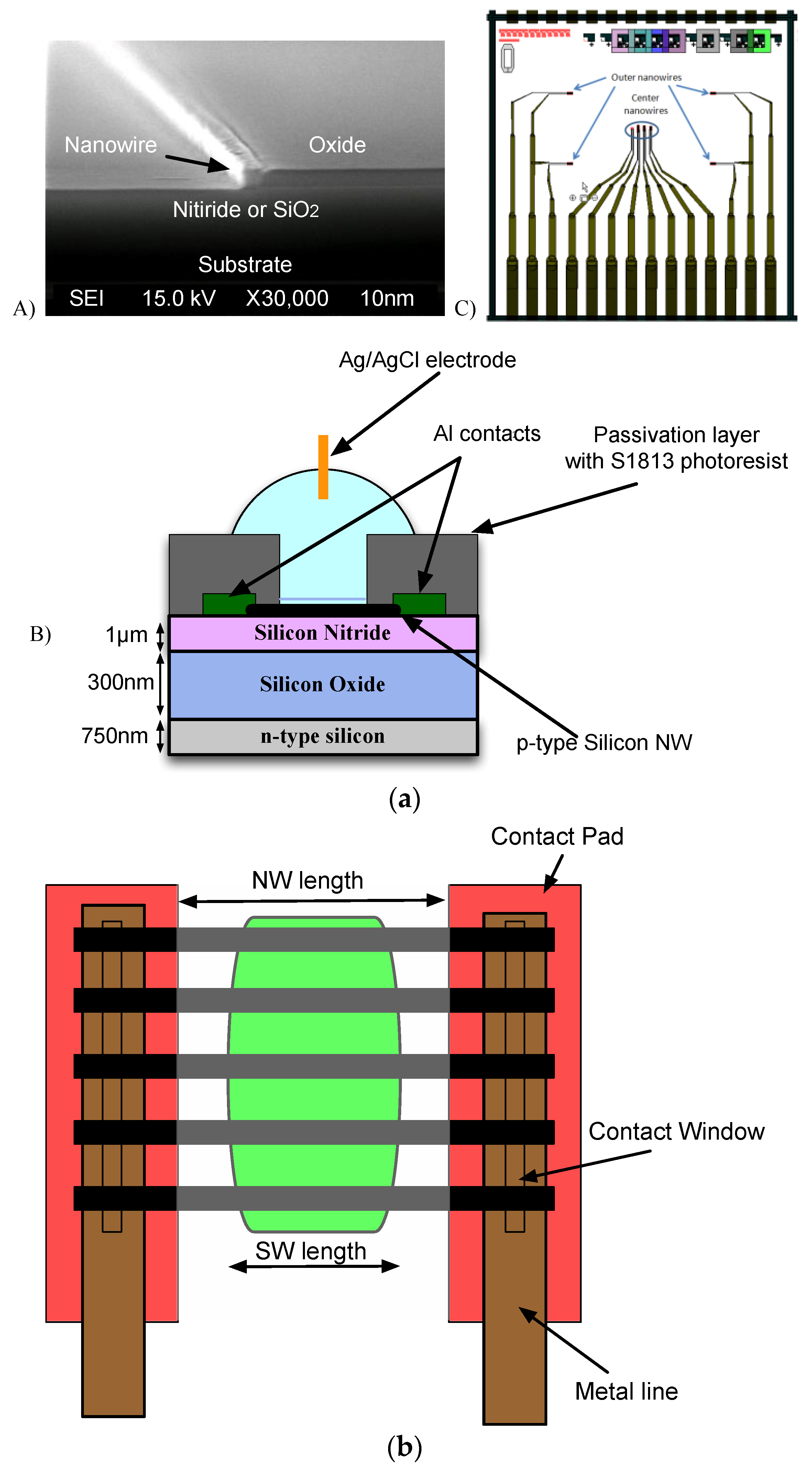
Figure 1. (a) Cross section of the nanowire: (A) SEM image of a fabricated polysilicon nanowire; (B) cross sectional diagram showing the different layers; (C) Layout of a NW chip showing connection pads compatible with standard commercial connectors; (b) Top view of a single NW device. Different numbers of nanowires (from 10 to 320) are connected in parallel depending on the nanowire set. The green area is the sensing window. The remainder of chip is covered with a layer of photoresist. The red area is the source/drain pads.
Biosensors 06 00015 g001
Figure 2. The solid-liquid interface showing the electrical double layer (EDL), the Debye length and electrostatic potential over the entire structure (from electrolyte to nanowire). A simplified version of the equivalent electrical model given by [34,35] is shown on the left, for the case of a small surface potential. CDL, CA, COX, CB are the double layer, surface chemistry, oxide, and bulk capacitances, respectively. RSOL is the solution resistance and RNW is the NW resistance.
Biosensors 06 00015 g002
Figure 3. (A) DC-sensing model described in previous section; (B) AC-sensing model defined by composing a distributed model element based on previous one; (C) Compact representation of the AC-sensing model; (D) Complex impedance sensed in or approach.
Biosensors 06 00015 g003
Figure 4. Typical experimental setup with the buffer potential fixed with a liquid gating electrode and substrate connected to ground. A stimulus voltage is applied at the source and a current read by a transimpedance amplifier at the drain.
Biosensors 06 00015 g004
Figure 5. Scheme describing a lock-in technique.
Biosensors 06 00015 g005
Figure 6. Representation of the adaptive two stage low pass FIR filter implemented in the LabView interface.
Biosensors 06 00015 g006
Figure 7. Pictures of the signal acquisition system.
Biosensors 06 00015 g007
Figure 8. Drawings of the nanowire chip holder highlighting the different components stacked in a “sandwich approach”.
Biosensors 06 00015 g008
Figure 9. Distributed model of the nanowire channel (A) and AC sensing model (B). Comparison of the SPICE model with experimental data (bare nanowires) in impedance module (C) and phase (D). RNW = 3 MΩ, CL = 5 pF, Cstray = 30 pF, CS = COX//CDL = 15 pF, CB = 100 fF, RSOL = 2 MΩ.
Biosensors 06 00015 g009
Figure 10. (a) Change in the surface charge at pH = 7 for different surface chemistry. The surface is deprotonated for both bare and succinic treated NWs while it is slightly protonated for APTES treated NWs; (b) DC measurements on NWs with different surface chemistry, pH = 7.
Biosensors 06 00015 g010
Figure 11. (A) AC impedance magnitude and (B) phase measurements showing how different surface chemistries can be discriminated. Simple DC measurements show no difference; (C) Cole-Cole plot of the same data.
Biosensors 06 00015 g011