Review

Ten Years Progress of Electrical Detection of Heavy Metal Ions (HMIs) Using Various Field-Effect Transistor (FET) Nanosensors: A Review

by
Shaili Falina
1,2,
Mohd Syamsul
2,3,*,
Nuha Abd Rhaffor
1,
Sofiyah Sal Hamid
1,
Khairu Anuar Mohamed Zain
1,
Asrulnizam Abd Manaf
1,* and
Hiroshi Kawarada
2,4
1
Collaborative Microelectronic Design Excellence Center (CEDEC), Universiti Sains Malaysia, Sains@USM, Bayan Lepas 11900, Pulau Pinang, Malaysia
2
Faculty of Science and Engineering, Waseda University, Tokyo 169-8555, Japan
3
Institute of Nano Optoelectronics Research and Technology (INOR), Universiti Sains Malaysia, Sains@USM, Bayan Lepas 11900, Pulau Pinang, Malaysia
4
The Kagami Memorial Laboratory for Materials Science and Technology, Waseda University, 2-8-26 Nishiwaseda, Shinjuku, Tokyo 169-0051, Japan
*
Authors to whom correspondence should be addressed.
Biosensors 2021, 11(12), 478; https://doi.org/10.3390/bios11120478
Submission received: 13 October 2021 / Revised: 13 November 2021 / Accepted: 17 November 2021 / Published: 25 November 2021
(This article belongs to the Section Biosensor and Bioelectronic Devices)

Abstract

:
Heavy metal pollution remains a major concern for the public today, in line with the growing population and global industrialization. Heavy metal ion (HMI) is a threat to human and environmental safety, even at low concentrations, thus rapid and continuous HMI monitoring is essential. Among the sensors available for HMI detection, the field-effect transistor (FET) sensor demonstrates promising potential for fast and real-time detection. The aim of this review is to provide a condensed overview of the contribution of certain semiconductor substrates in the development of chemical and biosensor FETs for HMI detection in the past decade. A brief introduction of the FET sensor along with its construction and configuration is presented in the first part of this review. Subsequently, the FET sensor deployment issue and FET intrinsic limitation screening effect are also discussed, and the solutions to overcome these shortcomings are summarized. Later, we summarize the strategies for HMIs’ electrical detection, mechanisms, and sensing performance on nanomaterial semiconductor FET transducers, including silicon, carbon nanotubes, graphene, AlGaN/GaN, transition metal dichalcogenides (TMD), black phosphorus, organic and inorganic semiconductor. Finally, concerns and suggestions regarding detection in the real samples using FET sensors are highlighted in the conclusion.

1. Introduction

Heavy metals are naturally occurring elements, produced from natural sources such as volcanic eruption, rock weathering, metal corrosion and metal evaporation from soil and water. Increasing human anthropogenic activities, including mining, industrial, agriculture and metallurgical, have escalated the heavy metal ions (HMIs) accumulation in our environment. The HMIs from these sources accumulate in the air, in drinking water, on plants, in animals, on soil, and on the earth’s surface. Consumption of these polluted plants, animals and drinking water can transfer the HMIs to humans, resulting in bioaccumulation. The toxicity of HMIs has a greater impact on children than on adults. A higher dose of HMIs among children may induce organ damage and promote neurotoxicity, which may cause behavioral disorders, learning problems and impaired growth in children’s development [1]. The Environmental Quality Standards Directive List has registered arsenic (As), cadmium (Cd), copper (Cu), chromium (Cr), iron (Fe), lead (Pb), mercury (Hg), nickel (Ni) and zinc (Zn) as prime substances of concern in water quality [2]. HMIs are imperative for life in trace quantity; however, they are hazardous to human health at higher concentrations. Real-time and constant HMIs monitoring is thus critical, reaching low concentrations (<nM). Table 1 summarizes the limit value, toxicity and heavy metal sources for heavy metal ions.
FET chemical sensor and biosensor systems for HMI detection consist of different functional blocks to create and measure analyte-specific signals, as presented in Figure 1. In this system, the recognition element (such as antibody, single-stranded DNA, ion-sensing membrane, etc.) and the transducer are fundamental components. The recognition element enables the binding of the probes-target to generate a signal, which corresponds to the presence of the HMIs and its abundance. In the case of biosensors, the recognition element is often conjugated on a solid surface layer on the transducer by immobilization. A transducer is a material that is responsible for converting the quantitative or semi-quantitative information about the target into a measurable signal (e.g., current, potential, and temperature change). Graphene, carbon nanotubes and silicon are the popular choice as a nanosensor transducer. The potential of these semiconductor and a few other semiconductor materials as transducers in FET/chemiresistive sensor development will be discussed in detail, and their application in HMIs’ electrical detection approach is critically reviewed. To date, different transducer platforms have been used to develop chemical or biosensors for HMIs monitoring, and a significant number of recognition elements has been explored to realize a wide range of HMIs detection.
Conventional detection methods, including atomic absorption spectroscopy (AAS) [4], inductively coupled plasma-atomic emission spectroscopy (ICP-AES) [5] and X-RAY fluorescence [6], are often used to conduct HMIs monitoring. However, these detection methods mostly require bulky equipment and trained personnel to perform the analysis. Recent developments in the field of sensors have led to a renewed interest in the miniaturization of three electrode-based electrochemical and an optical biosensor [7,8,9,10,11]. The newer sensor technology certainly offers the portability of the sensor and is more convenient to use. Nevertheless, most of the three electrode-based electrochemical and fluorescent sensors (regardless of size), require additional reagents for sensing operation, which limits their application as standard and simple analytical tools. Three-electrode electrochemical sensors require a redox mediator to assist the electrochemical activity on the electrode surface. It should be noted that the selection of a mediator could largely affect the sensitivity and selectivity of the electrochemical sensor. A previous study reported that the mediator may react with the heavy metal ions during the assessment, consequently influencing the accuracy of the electrochemical sensor [12]. In the case of a fluorescent biosensors, its sensing operation often requires pre-labelling the target with fluorescent dye [13]. This pre-labelling step in the fluorescent sensor complicates the assay procedure. When compared to electrochemical and fluorescent biosensors, FET biosensors assure rapid and accurate detection without the needs for additional reagents in their analytical assay. Therefore, the FET biosensor has the advantage of simpler handling for on-site application.
There are several types of commercially available HMI sensors on the market, including color test strips and color reagent kits (https://www.simplexhealth.co.uk/product/heavy-metals-test-kit-presence-1-test/, accessed on 16 November 2021) [14]. Both test kits change color with the presence of certain heavy metal ions. Even though it is considered cheap and convenient, there are several drawbacks associated with this kind of detection. Firstly, the test result reading is based on the color chart provided by the manufacturer, which can sometimes be misread by the user. Secondly, the reagent color only changes with the presence of heavy metal ions above µM (Cd = 44.80 µM, Cu = 78.69 µM, Pb = 24.13 µM, Hg = 24.93 µM, Ni = 85.19 µM, Zn = 76.45 µM, etc.) [14]. Finally, this colorimetric test cannot perform multiplex sensing, where the color reagent will turn grey in the presence of more than one species of HMIs at the same time. For these reasons, electrical detection, such as FET-based sensors, appears to be the most promising alternative to existing commercial HMIs sensors. FET offers rapid detection and accurate test results. Moreover, with appropriate receptors, the FET sensor allows for detection of HMIs at levels below nanomolar (nM). Multiple HMI detection is very possible with FET array sensors.
The past 50 years have seen increasingly rapid advances in the field of FET-based sensing since it was first introduced by P. Bergveld [15] for measuring ions’ activity in an electrolyte in a short communication dating back to the 1970s. The ion-sensitive FET (ISFET) derived from the metal-oxide-semiconductor FET (MOSFET) with the metal gate was removed and the gate terminal of the ISFET was governed by a reference electrode inserted into an aqueous solution, which is in contact with the underlying metal gate oxide. The earliest research on ISFET focused on monitoring ion concentration in a solution [16,17,18]; however, 12 years later, ISFET has been employed as a biosensor. For example, Janata et al. developed immunoFET for detection of anti-syphilis and anti-albumin antibodies [19]. To date, a vast body of literature has reported the work on ISFET with various types of gate-modification techniques, electrode materials, and sensing membranes. Not limited to biomolecular sensing, considerable efforts have been made to develop ISFETs for HMIs detection. Due to changes in gate modification or sensing membranes, ISFETs evolved into a variety of shapes and sizes, including the solution-gate field effect transistor (SGFET), chemical sensor FET (Chem-FET) and extended gate FET. The developments in the field of semiconductor fabrication have led to a renewed interest in FET-based sensors.
This review aims to provide an overview of Chem/BioFET sensor studies that have been dedicated to HMI detection for the past 10 years (from 2010 to present). To best of our knowledge, there are many reviews on the development of electrochemical [20,21,22], voltammetry [23,24,25] and fluorescence [26,27] HMI sensor; however, the review specifically on the electrical detection of HMIs is scarcely available in the literature. This review has been prepared in a way that comprehensively covers the information about all the aspects of the Chem/BioFET sensor, which could be useful to provide insights for researchers and scientists to accelerate their innovation for the detection of HMIs. This review begins with an introduction to FET, followed by the configuration and general FET setup. The FET intrinsic issues (screening effect and the Debye length) and their solutions to overcome these shortcomings are discussed in the next section, besides addressing the challenges of the FET sensor deployment. The following section will discuss the development of FET for HMIs sensing based on the types of semiconductors (silicon, carbon, III-V compound, transition metal dichalcogenide (TMD), and other materials, such as black phosphorus, organic-based FET and inorganic-based FET). Finally, the current challenge of using FET sensors for detection in real samples and suggestions to address the issue will be highlighted.

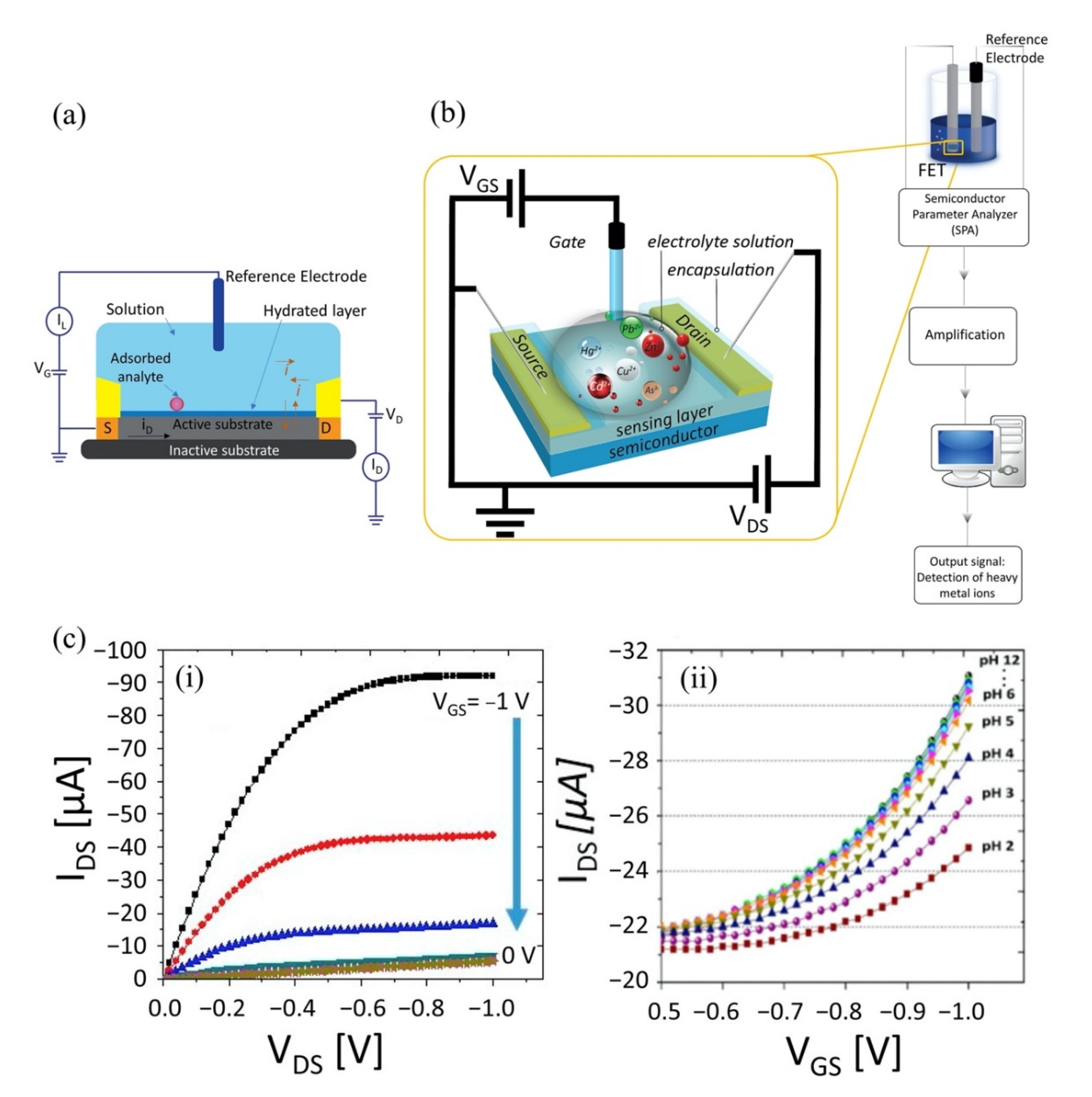
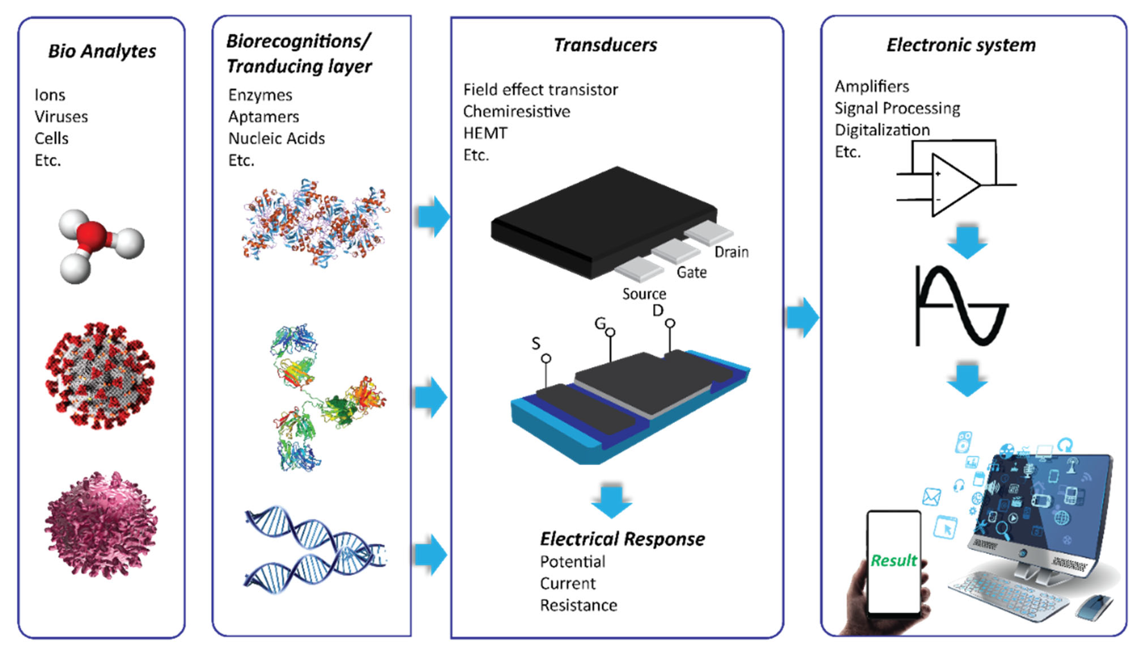
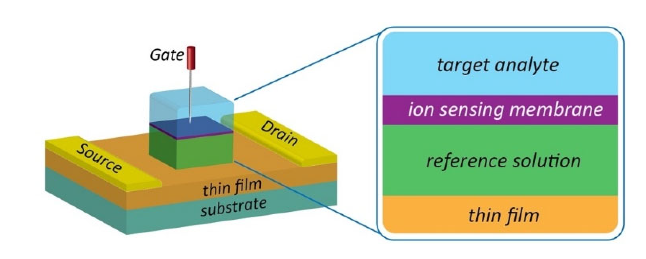
2. FET Configurations and General Experiment Setup for Electrical Detection of Heavy Metal Ions

Electrical detection of HMIs involves the use of FETs to generate a measurable electrical signal corresponding to the interaction of HMIs on the FET channel sensing interface. When the HMI bounds onto the channel area and creates an ionic bond with the sensing material, the surface potential changes, subsequently inducing charge accumulation near the semiconductor/analyte interface, thus modulates the carrier density in the channel area. For example, the negative ions on the sensing surface of an n-channel FET repel the electron carriers in the channel, resulting in a decrease of drain current, thus reflecting a low output signal. However, positive ions that are bound on the sensing surface will attract more electrons in the channel area, so there will be an increase in drain current. While explaining the detection mechanism of an FET in this manner appears to be straightforward, in practice, a few other parameters are involved, including the screening effect, the Debye length and the gate capacitance discussed in Section 3.
A typical FET configuration comprises three terminals: source, drain and gate, as shown in Figure 2a. The source and drain are symmetrical metal pads separated by a narrow channel area. In the FET setup, a voltage is applied at the drain (D) to enable current flow from the source to the drain terminal. While a gate voltage is applied at the gate, terminal (G) produces field-effect to control the current flow, and the source (S) terminal is usually connected to the ground. For HMI detection, the FET sensor is designed to adapt to the aqueous environment as most detection is carried out in solution. The FET that operates in an aqueous/electrolyte environment is customarily known as a solution-gate field-effect transistor (SGFET) or an electrolyte-gate field-effect transistor (EGFET). Both the source and drain of the SGFET/EGFET are passivated with waterproof materials to prevent ions from the analyte penetrating the circuit, while the metal gate electrode is replaced with a silver chloride (AgCl/Cl) reference electrode to control the field-effect between the source and drain terminals. The channel area is modified with a specific sensing interface or probe, such as nanoparticles, deoxrybozyme (DNAzymes), proteins, and aptamers for detection purposes. The selectivity and sensitivity performance of the SGFET/EGFET sensor is determined by the sensing interfaces. A typical FET sensor device requires gate dielectric layers to avoid unstable potential and impedance at the semiconductor/analyte interface. Earlier, silicon dioxide (SiO2) was a popular material used for the gate dielectric and semiconductor/liquid interface because of its stability when in contact with the electrolyte [28]. However, researchers eventually replaced SiO2 with other oxides (Si3N4, Al2O3, or Ta2O5) due to drift issues [29]. It is worth noting that some of the FET sensors, such as graphene SGFET [30,31] and diamond SGFET [32], allow for direct detection without requiring a gate dielectric or insulating interface. In such cases, the recognition probes are affixed directly on the semiconductor surface.
The electrical detection of HMIs in the laboratory is illustrated in Figure 2b. The setup consists of a SGFET sensor immersed in an analyte that contains HMIs, the AgCl/Cl reference electrode is used to supply gate voltage (VG), and external voltages to supply the excitation signal at the drain and gate terminals simultaneously to measure the sensor response. A semiconductor device parameter analyzer is used for this purpose. Voltages at the drain and gate terminals are varied, depending on the respective semiconductor material potential window, whereas the source terminal is kept constant (grounded). The electrical signal response upon detection of HMIs can be observed with the changes in the current-voltage characteristics of the SGFET sensor. Figure 2c(i) is an example of the current-voltage characteristics of a SGFET with p-type behavior, measured with gate voltage (VGS) values from 0 V to 1 V with 0.2 V of step (ΔVGS), while in Figure 2c(ii) is an example of changes in current-voltage characteristics of the SGFET sensor at different pH values (pH 2 to pH 12). HMI detection in a significantly low analyte concentration results in weak signals, hence amplification is needed prior to sending the response signal to any handheld device reader to interpret and analyze the recognition event. The amplification strategy is imperative to improve the signal-to-noise ratio (SNR) to detect target analytes in the case of high extrinsic noise. The silicon nanowire FET biosensor with rolling circle amplification (RCA) strategy exhibited an impressive signal-to-noise ratio (SNR) of >20, which could simplify the demand on the readout system [33].

3. FET Sensor Challenges

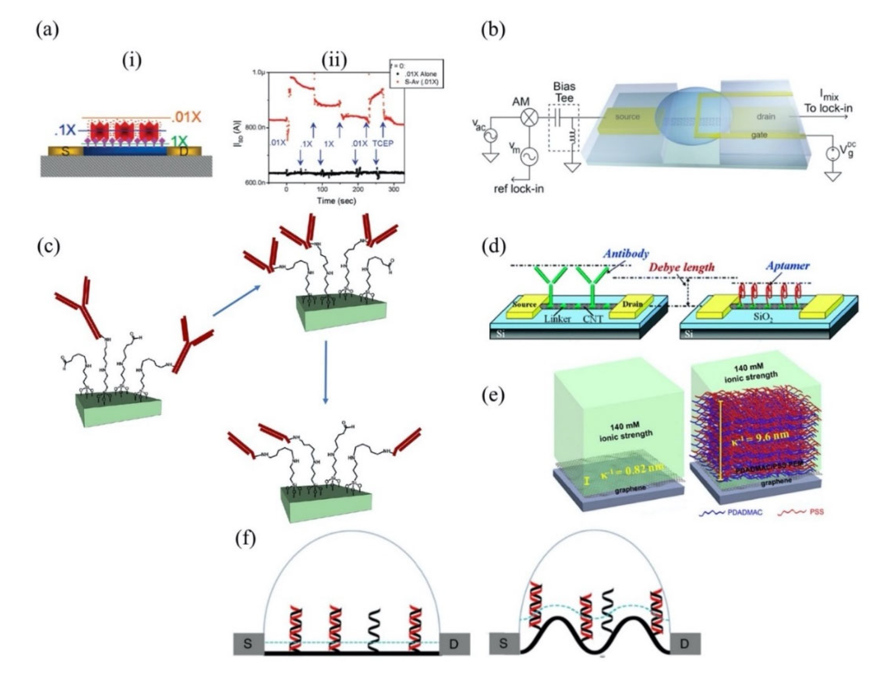
3.1. Screening Effect and Debye Length

Over the past decade, there has been exciting progress in FET sensor development. Researchers report various FET sensing interface designs that can specifically bind to the target of interest [35,36]. However, the sensitivity of the FET sensor is limited by the ionic screening effect, which remains a challenge, especially in high ionic concentration solutions (10× phosphate buffered saline) or physiological conditions. When a semiconductor solid surface is in contact with an electrolyte, some of the free mobile ions in the electrolyte approach the semiconductor surface and rearrange themselves as one layer of screening ions, creating an electric double layer, EDL. At a Debye length of ~1 nm (comparable to 100 mM in ionic concentration), the target charges can be electrically detected on the sensing surface [37]. However, when a captured target charge is located at a distance further than the Debye length, the electrostatic potential is shielded by these screening ions; therefore, the FET sensing surface could not detect this binding event. Moreover, the Gouy–Chapman–Stern diffuse double layer model advocates that the mismatch in size between Debye length and the target analytes’ charge would hinder the detection at the sensing surface [38]. Generally, in physiological conditions and high concentrated solutions, the Debye length appears to be short (~0.7–1 nm) [39]. Whereas most of the target charges are in medium-sized and large-sized molecules (the size radius can be up to 10 nm). Both circumstances contribute to a challenge in FET real-time detection in clinical samples. This section will discuss the Debye screening length and approaches that have been explored to overcome this limitation on the FET sensor. We note that the approaches presented in this review are not limited only to HMIs detection, but also include methods and strategies to overcome screening effects in general.
The sensitivity of a FET is strongly correlated with the Debye length. Certainly, the Debye length is an important parameter to be considered when designing a FET sensor. Many efforts have been made over recent years to overcome this FET shortcoming. A common technique to reduce screening effects is by diluting the test sample with buffer solution to reduce ion concentration [40]. A study by Stern et al. demonstrated the sensitivity of the FET sensor is significantly improved in low-concentrated electrolyte compared to a high ionic strength solution [41]. Figure 3a(i) elucidates the relationship between Debye length and ionic strength according to Stern et al. A 10-fold decrease in ionic strength extends Debye length from the device surface. Biotin-functionalized FET sensor for the detection of streptavidin has confirmed that the dilution of an electrolyte affects the Debye length. The sensor response depends on ionic strength resulting from different Debye lengths, as shown in Figure 3a(ii). While this method is effective for minimizing the screening effect, it also affects the binding of ligand–protein and protein–protein interactions. Therefore, this method is impractical for real-time detection. Kulkarni et al. exploited high transconductance silicon nanowires (SiNWs) to operate the FET sensor at high frequency [42]. This method presents outstanding sensor performance in highly concentrated solutions up to 100 mM. However, the complex sensor device geometry complicates its application in cellular or vivo sensing, as shown in Figure 3b. A study by Elnathan et al. [43] found that the fragmentation of biorecognition probes can improve the sensitivity of FET sensors in physiological conditions such as serum and blood without sample pre-treatment. In the study, Elnathan disintegrated antigen binding from antibodies for detection of proteins to reduce the size of the sensing probe, so that it is closer to the sensing surface and falls within the Debye screening length for high sensitivity detection. Figure 3c illustrates two steps in which the antibody degrades into fragments to reduce the antibody receptor size as proposed by Elnathan. One way to diminish the screen effect is the use of aptamers as biorecognition probes. Because the size of the aptamer is smaller than the Debye length (Figure 3d), this allows for binding events to occur within the electrical double layer and yields a high sensitivity sensor response. On this basis, Maehashi et al. developed an FET sensor functionalized with aptamer for immunoglobulin E (IgE) detection [44]. In another report, the use of polyelectrolyte layers effectively increased the sensing range, as depicted in Figure 3e. Paccinini et al. introduced PDADMAC/PSS polyelectrolyte multilayer (PEM) films on the graphene FET sensor to increase the sensing range [45]. Interestingly, the Debye length was found to increase from 0.8 to 10 nm, enabling detection of bigger biomolecules. Furthermore, Lieber et al. suggested the use of a biomolecule-permeable polyethylene glycol (PEG) polymer layer on the SiNWs FET sensing area to extend the Debye length in high ionic strength solution [46]. They showed the FET sensor device with PEG-modified exhibits real-time detection of prostate specific antigen (PSA) in concentrations as high as 150 mM. To validate their hypothesis, the outcome was compared to the performance of the FET sensor without PEG-modified as the control, and it was found the control only enables detection of PSA in concentration ≤10 nM. In this study, it was proven that the FET sensor with a PEG layer is effective for PSA detection and demonstrates real-time detection in a 1× PBS solution, which mimics the physiological environment. A recent study showed that the screening effect of an FET can be reduced using rippled sensing area (channel). The study particularly demonstrated the crumpled (deformed and bent) graphene FET biosensor for ultrasensitive detection of DNA/RNA molecules [47]. The crumpled form of graphene was attained by manipulation of the two-dimensional (2-D) layer with controlled heat to induce deformation of the underlying substrate. With a crumpled sensing surface, the Debye length fluctuated at the peaks and the valleys, as shown in Figure 3f. The performance of the crumpled graphene FET as a biosensor was compared with that of the flat graphene FET, which was used as a negative control. The first set of analyses examined crumpled graphene FET responses in different pH solutions. Compared to the control group, the crumpled graphene FET demonstrated a larger shift in Dirac point from pH 3 to pH 11. Turning now to the experimental evidence on DNA sensing of crumpled graphene FET in DNA solution, the flat graphene FET showed a total Dirac point shift of 80 mV, whereas the crumpled graphene FET exhibited a total Dirac point shift up to 180 mV. They further evaluated the performance of the crumpled graphene FET sensor in a clinical sample (undiluted human serum) to detect miRNA. Even in high ionic and complex matrices of biological components, the sensor demonstrated excellent potential as a highly sensitive biosensor, which showed detection of miRNA molecules in the human serum as low as 20 aM of concentration. These experimental data have supported the hypothesis that the screening limitation of a graphene FET can be eliminated by using crumpled graphene on the sensing area. Their computational simulation data revealed that the fluctuated area (peaks and valleys of crumpled graphene) had higher DNA adsorption energies, especially on the concave area (−532.187 kcal mol−1). They deduced that the extraordinary performance of the crumpled graphene FET sensor was contributed by these valleys’ regions (concave areas). Due to the nature of a concave region with deep and narrow trenches, the free mobile ions in the tested solution were excluded and farther away, which allowed the DNA to get closer to the graphene surface, thereby inducing more graphene carrier density, resulting in a larger Dirac point shift. However, this method is only applicable to 2-D materials or thin films that can create ripple effects.

3.2. Sensor Deployment

Sensor portability is a popular solution to conventional benchtop laboratory sensors for ease of implementation and cost-effectiveness. Recent advancements in nanoscale devices have led to the miniaturization of biosensors, which show promising potential to be deployed as self-contained lab-on-chip devices. While the research of nanosensors in the laboratory shows significant sensing performance, several important challenges remain to be addressed before the portable sensors can be deployed on a large scale. In this review, the focus is on three challenges to deploy FET sensors, which are in terms of selectivity, platform integration/reading and real-time measurement.
The important aspects concerning a sensor are sensitivity and selectivity, which are determined by the recognition elements or receptors on the sensing surface. An appropriate sensor receptor must be carefully chosen to obtain a high sensitivity sensor. With regard to selectivity, the recognition elements often show cross-selectivity with interference ions in complex matrices. In general, the lower the detection limit is required, the more difficult for a sensor to identify a specific target in the given matrix, so the sensor may give misleading (false positive) results. This is an important issue that needs to be addressed, especially for self-operating system sensors. One possible solution is to fabricate the sensors in an array for multiplex detection, in which each sensor is functionalized with different receptors. The sensor signal would contain a vector of responses, which is treated as a detection pattern by the end users. In this way, false results can be avoided when the samples of complex matrices are assayed. The conventional approach to realizing multiplex detection is to fabricate a multiple-channel FET either with a one-shared gate terminal or an individual side gate terminal on each channel to allow individual access to each FET [48]. In this approach to sensing multiple target ions, each FET channel is immobilized with different biorecognition molecules. A proof-of-concept study demonstrated multiplex detection of prostate specific antigen (PSA) and PSA-α1-antichymotrypsin (PSA-ACT) with a silicon nanowire FET array [49]. The individual FET sensor devices were modified with different monoclonal antibodies (mAbs) that corresponded to the target proteins. The first FET (NW1) was functionalized with mAbs for free PSA (Ab1). While the second FET (NW2) was functionalized with cross-react mAbs of free PSA and PSA-ACT (Ab2). This study found that the FET conductance changes were observed in both NW1 and NW2 when free PSA was introduced to the sensor. The introduction of PSA-ACT yielded conductance changes only in NW2, suggesting specific binding of PSA-ACT on the sensor device NW2. These findings suggest that the FET sensor array has the potential for multiplex detection of free PSA and PSA-ACT proteins at the same time. The study also investigated the selective detection of either cancer biomarker in a single real-time assay, with the help of an additional blocking solution to block off the other target. For example, a solution of Ab1 was mixed into the mixture of free PSA and PSA-ACT solution before being introduced to the sensor array to block off the free PSA target, resulting in conductance changes in NW2, but not in NW1.
Most single chemical- and biosensors (including FET) exhibit limitations in multiple detections in complex matrices. As demonstrated above, they can only be used to determine one or two types of analytes simultaneously. Therefore, a multisensory system is needed to overcome this challenge. Such a sensor system has been widely studied and recognized as electronic tongue (e-tongue) [50]. Generally, e-tongue was developed to mimic human chemical senses for liquid analysis, especially for food and beverages. However, its application to date has extended to biology, pharmaceutical and environmental fields. The e-tongue is comprised of poorly selective and lower-specificity chemical sensor arrays coupled with pattern recognition math methods (PARCs) to analyze multiple target analytes simultaneously. Common e-tongue pattern recognition uses chemometric tools, which have been used to translate hundreds or thousands of signal data onto visualization maps [51]. E-tongue is a promising low-cost detection system, and it can be integrated into the internet of things (IoT). Additionally, the combination of e-tongue with a pattern recognition algorithm is a powerful analytical tool for the rapid and accurate detection of ions in complex media. From our perspective, the performance of e-tongue cannot be compared to that of a FET biosensor, as e-tongue is a complete sensor system, while FET performance is often evaluated at a single device level. However, a FET biosensor can be incorporated into an e-tongue system to achieve rapid and accurate multiple detection. Several studies attempted to develop FET ion sensors towards e-tongue applications [52,53,54]. The e-tongue for heavy metal ions detection has been comprehensively discussed elsewhere [55].
Detection of low abundance of HMI in a real sample can be divided into two steps: (1) separation of high-abundant non-specific target molecules and (2) increasing efficiency of mass transfer target (HMI) to the sensing area. A common problem faced by a biosensor assay in a raw sample is being unable to distinguish between target and non-target molecules. Therefore, the target molecule needs to be isolated from non-specific molecules before being analyzed by a biosensor. It has been demonstrated that the detection of raw samples that undergo a separation step prior to introduction to a biosensing surface is more efficient [56]. The separation of the target molecules can be realized with different tools/techniques, such as micromixing [57], immunomagnetic beads [58], dielectrophoresis (DEP) [59], filtration [60] and centrifugation [61]. Among these separation methods/techniques, centrifugation is popular for isolating target molecules due to its simplicity and efficiency compared to the other methods. Although centrifugation could not separate the HMI-contaminated solution into different ion species; however, it could aid in the separation of HMI from complex water matrices [62,63,64,65]. One significant advantage of the centrifugation step in the HMI detection assay is that it discards impurities and interfering non-target species on the sensor surface, thereby promoting better selectivity of the sensor. Moving on to look at DEP implementation in biosensors to improve the sensitivity and selectivity of the biosensor assay. In brief, DEP is a non-uniform electric field that is applied to the biological fluid to manipulate the position of the biomolecules in a given region. The inhomogeneity of DEP imposes a net force on biomolecules and pushes them towards/off the electric field region depending upon the polarization between biomolecules and the suspending medium. The DEP force is particle size dependent, which helps to separate molecules into different regions based on their type. This technique is particularly useful for concentrating the target sample on the recognition probe to enhance the sensitivity of a biosensor [66]. DEP can also be used to filtrate and purify the biology target samples [67], to discriminate between specific and non-specific bindings of biology components [68], and to deposit biological targets onto desired the location on sensing platform of field-effect based biosensor [69]. In FET application, one study reported DEP for pre-concentrated deoxyribonucleic acid (DNA) analyte on poly-silicon nanowire field-effect transistor (poly-Si NWFET) [70]. In this study, a three-dimensional (3-D) microstructure of poly (ethylene glycol) diacrylate (PEG-DA) was used to shape the electric field on the micro-constricted fluid channel onto the poly-Si NWFET sensing region. The DNA pre-concentration degree increased by 4-fold, 5-fold, and 4-fold in the constriction channels of 6, 10 and 20 µm, respectively. The gate voltage of the poly-Si NWFET sensor shifted by 0.5 V when a DEP condition of 30 Vpp (peak to peak) at 500 Hz was applied for 5 min to a double stranded DNA analyte (20 bp) of 1 nM concentration in sodium phosphate buffer of 10 mM concentration (pH 7). The gate voltage shift suggests increased sensitivity of the poly-Si NWFET.
Another selectivity sensor challenge is closely related to non-specific binding (NSB), a common issue faced by nanomaterial-based sensors, because a small degree of NSB affects the sensor sensitivity substantially. This can be mitigated to a certain extent by the use of PEG-containing polymers as the coating layer on the FET channel surface. The sensing receptors can be affixed on the PEG-coated surface covalently. The PEG-coating provides a high hydrophilic surface and is charge-neutral, thus banishing the hydrophobic interaction of unwanted ions on the FET channel surface. However, this may change the FET channel surface properties [71].
The rapid growth of microfluidic technologies has made the lab-on-a-chip (LoC) FET sensor possible. In general, the system requires fluidic handling to transport the solution of interest to the reaction zone and subsequently makes contact with the FET sensor receptors or probes to selectively capture the target. A transduction mechanism is required to convert the FET sensor responses to electrical signals for the end user to view the results. However, to get an accurate analysis, sample preparation and pre-treatment are necessary for this system. Sample preparation is essential to remove contaminant ions in the analyte of interest and to extract target analytes. A major challenge in microfluidic systems is the complexity of the sample preparation. Too large particles may clog up the micron-sized microfluidic channel. In real-life applications, one size microfluidic channel does not fit all heavy metal ions. Non-specific absorption on the microfluidic wall is another concern that needs to be addressed, because it may result in non-specific signals, changes in flow behavior, and channel clogging [72]. Beyond that, the integration of the microfluidic system and the FET sensor must be seamless to justify the claims of high sensitivity and rapid response times, as this includes the sample preparation period. In regard to sensor signal reading, choosing a strategy for signal amplification is quite a hurdle, as the presence of the target is mostly at trace levels. The amplification strategies have been highlighted in the literature [73,74]. Although the amplification strategy does increase sensor sensitivity, nevertheless, this comes at the expense of an increase in analysis time and complexity. Moreover, an amplification strategy with complex procedures tends to increase the chance of errors and reduce reliability.
Another issue is real-time measurement without cleaning the sensor surface or changing the sensor. Besides the specific target binding, NSB from analyte components tends to adhere to the sensor surface. Both specific target binding and NSB give rise to biofouling, which forms an impermeable layer that inhibits the sensor surface, resulting in false readings and impeding the sensor’s reusability. Biofouling affects sensor performance in terms of sensitivity, stability, reproducibility and reliability [75]. In any case, the FET sensor requires anti-fouling strategies or a self-cleaning surface to avoid surface effects for real-time measurement. A number of publications have proposed anti-fouling strategies to alleviate the biofouling problem on the FET sensor channel surface. For example, Yang et al. used covalent organic frameworks (COFs) to encapsulate the FET sensor channel to prevent it from being fouled [76]. COFs are crystalline mesoporous polymers [77] that allow modification and functionalization on their large specific surface area. Yang et al. reported that the FET sensor performance with anti-fouling COFs was comparable to that of a FET sensor without anti-fouling property. This anti-fouling approach is convenient for FET sensor construction. Another anti-fouling strategy is to separate the sensing surface that accommodates the target analytes from the measuring surface. However, this strategy is only applicable for FET sensors with side gate [78], floating gate [79,80] and dual-gate [81,82]. As an alternative to typical FET sensor construction, a semipermeable lipid membrane coating is used on the FET channel to separate the sensing surface from the target analytes and only allow the target of interest to reach the sensing area [83]. Deployment of the FET device as a monitoring tool for HMIs has to consider self-cleaning sensing surface for long-term use and reusability without compromising its performance. An advantage of the self-cleaning sensor is that it helps to avoid tedious treatment after being used. It is feasible by modifying the sensor transducer with a superhydrophobic and conductive nanocomposite. The nanocomposite superhydrophobicity property helps to mitigate absorption from molecules and oxidation in air, whereas its high conductivity property is very useful for enhancing sensor signals. Zhu et al. fabricated a self-cleaning sensor by implementing a superhydrophobic and conductive nanocomposite of polydimethylsiloxane (PDMS) and multiwall carbon nanotubes (MWCNT) on the sensor electrode [84]. They reported that the sensor electrode integrated with PDMS@MWCNT can be shelved for more than one month with no signal degradation and significant passivation. The sensor is reusable by simple washing. Besides conductive material, PDMS can be grafted with zwitterionic copolymer as a self-cleaning surface material. De Vera et al. grafted PDMS material onto poly (glycidyl methacrylate-co-sulfobetaine methacrylate-co-2-(dimethylamino) ethylmethacrylate) polymer, poly (GMA-co-SBMA-co-DMAEMA) to develop pH dependent self-cleaning surface [85]. Their findings confirmed the reversible attachment and detachment of microorganisms, which paved the way for reusable biosensors. However, the pH target analytes must be reconsidered as this material is pH dependent; therefore, the ionic strength of the analytes may affect the sensor response.

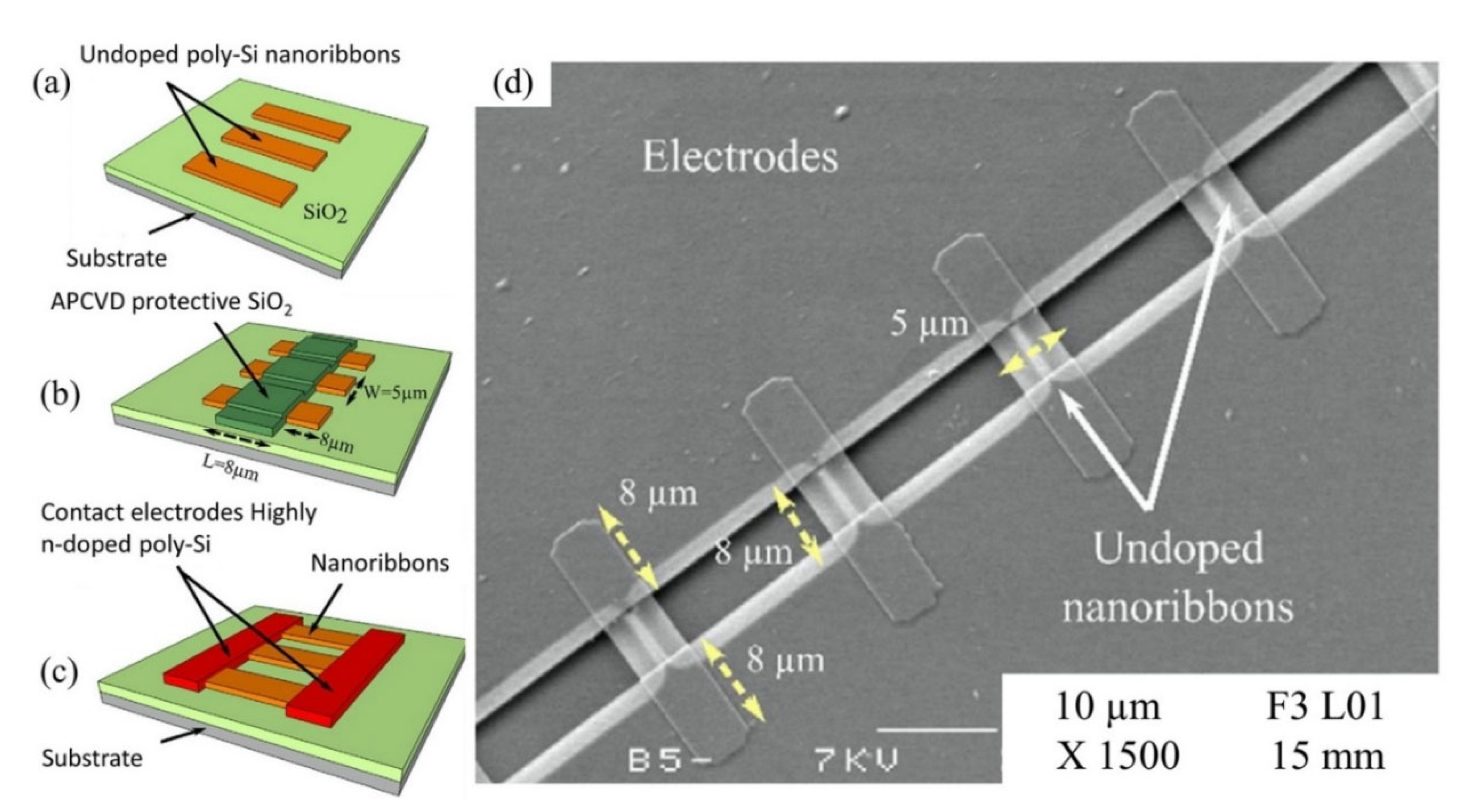
4. Silicon-Based FET

Silicon (Si) semiconductor has drawn great attention as sensor material due to its abundance availability and surface modification flexibility [86]. In addition, silicon can be manipulated into different nanostructures, such as nanowires, nanorods and nanoporous, which offer large surface areas to produce high sensitivity sensors [87]. Moreover, mature silicon technologies enable seamless integration with complementary metal-oxide semiconductor (CMOS) circuits for direct sensing systems [88]. Si materials have shown promise towards the evolution of FET biosensors since the seminal work by Bergveld in the 1970s [15]. To date, considerable efforts have been made to develop a reliable and high sensitivity silicon-based FET sensor for various ions’ detection, including heavy metal ions.
Nguyen et al. and co-workers investigated the potential of hydroxypyridinone derivative modified lipid as an active sensing layer on silicon FET for ferric ions (Fe3+) detection [89]. In this work, Nguyen used pyridinone-phospholipase (an enzyme) to modify an ultrathin (~3 nm) organic lipid to create a receptor compound that selectively binds with Fe3+. Subsequently, the modified lipid was absorbed onto the FET channel surface (Si-H) using the vesicle fusion technique, which is widely employed to create lipid layers [90]. Upon Fe3+ detection, the FET gate-source voltage shifted up to 200 mV, suggesting good sensitivity of the sensor. The most important finding was that the pyridinone-embedded FET sensor exhibited specific detection of Fe3+ in a wide detection range of 5 pM to 50 µM. The remarkable detection results are attributed to the high binding capability of hydroxypyridinone with ferric ions (Fe3+), which is in good agreement with a published article by Chaves et al. [91]. Further, the research group investigated γ-pyrone derivative engineered lipid as a pH-independent sensing layer on silicon FET for Fe3+ detection [92]. A commercial lipid was cleaved with an enzyme before being tethered to γ-pyrone for ferric ion detection. The thickness of the lipid layer was reduced to 2.7 nm to improve the sensor sensitivity. The diagram of the modified γ-pyrone derivative lipid layer is illustrated as in Figure 4a. The results of this study showed that the γ-pyrone monolayer lipid was pH-insensitive. The electrical property of the modified lipid layer was examined in different pH solutions. A commercial DCPC lipid was used in this experiment as a comparison to Nguyen’s γ-pyrone modified lipid. Figure 4b(i,ii) compare the lipid behavior in different pH solutions (pH 2–10). The DCPC lipid (blue) shows the current and VTH change across the pH, while Nguyen’s γ-pyrone modified lipid (red) exhibits a stable current and no VTH shift, especially in the pH range of 2 to 7. In their sensing studies, the γ-pyrone modified lipid FET sensor showed a relative response to Fe3+. This finding broadly supports the work of other studies in this area, linking the high affinity of γ-pyrone towards iron ions [93,94]. Their experiment data conclusively shows that the sensor response was not under pH influence and the modified γ-pyrone lipid layer is suitable to be used as a FET sensing element in medical diagnostic applications such as blood, sweat and urea, in which pH variations tend to occur, especially when patients are treated with drugs. This sensing strategy can discriminate Fe3+ from interfering ions in a concentrated solution as high as 50 GM and as low as 50 fM (detection limit). In another report, a modified lipid with di-2-picolylamine (DPA) was embedded in an FET channel for Cu2+ detection in a solution [95]. This is the first report showing a dual-gate FET sensor with engineered lipid monolayer for HMI detection. The lipid used in this assay was engineered to prevent ion trapping and provided sensor stability. The assay exhibited remarkable sensing potential with sensitivity of 98 ± 3 mV/decade, which exceeds the Nernst limit of 29.5 mV/decade predicted for divalent ion by a factor of three. The authors claimed that this super-Nernstian performance was attributed to dual-gate FET geometry, as the performance of their previous single-gated FET sensor merely exhibited Nernstian behavior [92]. Furthermore, this lipid FET sensor demonstrated exceptionally low limit detection at the femtomolar level (10 fM) and had sufficient specificity towards Cu2+.
A few nanowire silicon-based FET sensors for heavy metal detection have also been published in the literature. The majority of recent work in this field stems from the seminal work of Cui et al., who first explored the potential of SiNWs as a highly sensitive biosensor [96]. Cui and co-workers primarily demonstrated vapor-liquid-solid (VLS) grown SiNWs FET for ion detection, and later they carried out the experiment for the detection of streptavidin binding on the biotin-functionalized SiNWs surface. Their research on SiNWs as biomolecular sensors was extended to the detection of calcium ions (Ca2+). The SiNWs surface was immobilized with calmodulin as a receptor to recognize the Ca2+ ions. These studies have demonstrated the high potential of SiNWs as a material for biosensors. In recent years, there has been an increasing interest in SiNWs-FET for HMIs detection. Jin et al. demonstrated a free-standing SiNWs-based FET sensor that can detect mercury ion (Hg2+) as low as 4.985 mM [97] and has a wide detection window, in a linear range (R2 = 0.9838) between 4.985 mM and 24.926 nM. The sensors were fabricated in an array using the top-down method, which demonstrated the ability to exhibit high selectivity toward Hg2+ ions in real-time detection. The SiNWs electrode surface was functionalized with (3-Mercaptopropyl) trimethoxysilane (MPTMS), an organosilane with a thiol group as receptor to recognize Hg2+ ions. More interesting is that the type of SiNWs used in this investigation were inverted-triangle-shaped. With a highly controllable microfabrication process, the diameter size of the free-standing SiNWs was determined around 100 nm. This SiNWs geometry provided advantages in using all three facets as sensing areas. Therefore, this sensor configuration provided more thiol probes to bind with Hg2+ ions. Accordingly, the performance of the sensor was enhanced. Even though the sensor shows excellent sensitivity and selectivity, the reproducibility and stability data of the sensor were lacking. To address the stability issue, Huang et al. [98] from the same research group produced a better and more stable SiNWs FET-based sensor for the detection of Hg2+. The sensing strategy for this sensor was a little bit different than the previous sensor. With the aim of providing more thiols as sensing probes, the new sensor utilized gold nanoparticles (GNP), which were functionalized on the SiNWs surface with the aid of 3-Aminopropyltriethoxysilane (APTES). Subsequently, the thiol groups were immobilized on top of GNPs as receptors to bind with Hg2+ ions. The use of GNPs has increased the surface area and the number of thiol probes to amplify the response signal. The resulting sensor exhibited high selectivity and ultra-sensitivity of Hg2+ ions with a LOD of 0.06 pM and a wide range of detection of 1 ng/L–10 μg/L−1. Additionally, this sensor also demonstrated very fast response in unknown samples under 1 min. The use of DNAzyme on the SiNW-FET channel as a receptor for HMI recognition has also been reported with promising results. A simple approach for selective detection of silver ions (Ag2+) in aqueous on the basis of C-Ag2+-C coordination chemistry was proposed by Chen et al. [99]. The silver specific oligonucleotide (SSO), which richly contains cytosine mismatched base pairs (C-C), was grafted onto the SiNW FET device. When Ag2+ is introduced into the solution, the mechanism is primarily based on the formation of stable cytosine-Ag2+-cytosine, which converts a single-stranded SSO into a double helix structure. The helix structure accordingly increased the negative charges on the SiNWs surface, resulting in the conductance increased in gate oxide. With this sensing strategy, authors reported the detection of Ag2+ could be up to 100 μM, while the LOD of this sensor was 3 nM. Moreover, the DNAzyme/SiNWs FET sensor demonstrated a linear response with increasing Ag2+ concentration.
Other than SiNWs, silicon nanoribbons (SiNRs) are also receiving a significant amount of attention for biosensor fabrication [100,101,102]. It is a great alternative to SiNWs as a sensor transducer material because it offers compatibility with the top down CMOS process [103]. A recent example of an electrical assay to detect HMI with SiNRs was demonstrated by Synhaivska et al. The research group has designed a SiNRs ISFET functionalized with glysine–glysine–histidine (Gly–Gly–His, GGH), as illustrated in Figure 4c, for the detection of copper ions (Cu2+) [104]. The detection of the Cu2+ using GGH ligands is based on the conformational change of the ligands when the secondary amides are deprotonated in the presence of copper ions, leading to increases of negative ions near the SiNR surface. Figure 4d(i–iv) shows the response of the GGH functionalized SiNR FET sensor in high concentration Cu(NO3)2 solutions (0.05–10 mM) at pH 4, 5, 6, and 7. The sensitivity of the sensor at pH 4, 5, 6, and 7 was 11, 8, 3.9, and 14.1 mV/dec, respectively. These findings suggest that the sensor performance was pH dependent, and these observed results could be attributed to the protonation and deprotonation degrees of secondary amides at different pH. Interestingly, the GGH/SiNR-FET sensor gave a negative differential response in a neutral solution (pH 7), as seen from Figure 4d(iv). A possible explanation for this result was that in pH 7 solution, the Cu2+ ions dominated the interaction on the FET channel surface over hydroxyl (OH-) or hydrogen (H+) ions. The FET sensor demonstrated linear responses in varying Cu2+ concentrations (from 0.1 fM to 0.1 μM) at pH 7 solutions and reached LOD at 10 fM, which is exceptionally lower than any other HMI FET sensor that has been mentioned in this review. However, the main drawback of this sensing approach is that the deprotonation of the secondary amides in GGH by the pH media can limit the sensor application. Also, a poly-silicon nanoribbon resistor sensor grafted with aryl diazonium salts for sensing Pb2+ has been proposed [105]. Similar to a FET sensor, the resistor or chemiresistor type sensor changes its electrical resistance corresponds to potential changes on its channel surface, except that it does not involve field-effect to control the conductivity in the channel region. Construction of the poly-Si nanoribbon resistor sensor for Pb2+ sensing is shown in Figure 5a–c. The SEM image in Figure 5d shows the top view of the resistor sensor with a length and width of 8 µm and 5 µm, respectively. The sensing mechanism of this sensor relies on the positively charged Pb2+ ions that are attracted to negatively charged carboxylate groups (-COOH) on the SiNR surface, resulting in modulation of the quantity of charge flowing through the resistor. The surface functionalization of the poly-silicon nanoribbon FET is relatively easy. A simple dip in aqueous solutions that contain the recognition element for a certain period can give homogenous functionalization coverage on the silicon surface, in this case, aryl diazonium salts. The resistor sensor successfully detected the Pb2+ in a variety of concentrations, from 10 µM to 1 µM. Both of the poly-SiNR sensor devices reviewed in this paper are functionalization of the surface employed by the spontaneous grafting technique. Although the grafting method for SiNR surface functionalization is straightforward, the long exposure time of the SiNR-FET in the receptor contained solution could lead to over functionalization, which may produce a screening effect [106].
Silicon-alloy materials such as silicon carbide (SiC), silicon nitride (Si3N4), and silicon germanium (SiGe) have also been described for FET sensor development to detect biomolecules, ions, and DNA [107,108,109]. Although considerable advancements have been achieved in ion detection, the silicon-alloy-based FET sensor is scarcely explored for HMIs. From our observation, the research in this field has tended to focus on silicon nanostructures rather than silicon-alloy as a sensor material. This focus is because the dimensional similarity of the nanostructures and the subject to sense offers seamless integration of nanoelectronics and life sciences, which enables high sensitivity and revolutionizes the sensing and detection area.

5. Carbon-Based FETs

5.1. Carbon Nanotubes (CNTs) FET

Since its discovery in 1991 by Ijima [110], CNT material has attracted significant attention in scientific research. At the time, CNTs immediately became one of the promising materials for biosensor transducers owing to their physical and electrical properties. CNTs and graphene share many excellent properties, as CNTs are made of single or multiple layers of graphene rolled around seamlessly with the advantage of having an endless, perfect hexagonal structure. CNTs are a popular material with a large surface-to-volume ratio, which makes them a good semiconductor for high sensitivity sensors. One molecule of absorption on the sidewall of CNTs promotes a change in the local electrostatic environment, consequently changing its conductance [111]. Furthermore, its unique electronic transport properties have high potential for sensor device miniaturization. Its atomically thin structure gives it an advantage as an ideal electrostatic control over the channel, which is important for a miniature device sensor [112]. Additionally, on the account of its biocompatibility properties and size compatibility with a single molecule make CNTs an ideal platform for biosensing materials [113]. A large volume of literature has reported the application of carbon nanotube FETs for bio- and chemical sensors [114,115,116]. Over time, the CNT-based FET sensor has been constantly fabricated and its potential has been explored for different target detection.
RNA-cleaving DNAzyme is commonly employed for sensitive and selective HMI detection in biosensors or chemical sensors. DNAzyme possesses unique chemical properties that selectively bind to specific metal ions with multiple turnovers, making it an ideal recognition element [117]. DNAzyme in general consists of an enzyme strand and a substrate strand. The latter accommodates a single ribonucleobase (RNA) linkage functioning as a cleavage site. In the absence of targeted metal ions (cofactor), these two strands are hybridized to form a double helix in buffer solution. While in the presence of the target metal ions, DNAzyme cleaves the substrate strand, releasing a shorter fragment from the duplex. The change in DNAzyme structure can be used to induce the carrier accumulation numbers in nanomaterials. Thereby, DNAzyme is very convenient to be used as an FET sensing probe. DNAzyme being used in other sensing platforms has recently been reviewed elsewhere [118,119].
The group of Wang et al. has made a tremendous contribution to the detection of HMIs based on the single-walled carbon nanotubes (SWCNT)-FET sensor platform. Most of his HMI detection work exploited metal-dependent DNAzyme and aptamer as sensing elements on SWCNT-FET sensors. In 2018, the research group demonstrated a CNT-based FET functionalized with silver specific RNA-cleaving DNAzyme for the detection of silver ions (Ag+) [120]. The FET structure and SEM image of the sensor are shown in Figure 6a(i,ii), respectively. In the presence of Ag+, the substrate strand was fragmented and released from the RNA-base, leading to a change in DNAzyme’s structural and, subsequently, the change the electrical conductivity of the CNT-FET. This sensor exhibited high sensitivity and selectivity towards Ag+ at a linear response range of 101 pM to 106 pM (Figure 6b). The Agzyme/SWNTs-FET sensor’s selectivity was determined by testing the sensor response in various ions found in water environments, including Na+, K+, Pb2+, Mn2+, Cd2+, Zn2+, Cu2+, Ni2+, Ca2+, Fe3+, Al3+ and Cr3+. The result indicated that the Agzyme/SWNTs-FET sensor exhibited the highest relative resistance change in Ag+ solution, suggesting that it has excellent selectivity towards Ag+. The Agzyme/SWNTs-FET demonstrated resistance to change in the Pb2+, Cd2+ and Cu2+ solutions, but the values were less than 5%, as shown in Figure 6d. The limit of detection of 5 pM was obtained. Further, the Agzyme/SWNTs-FET was investigated in a real river water sample. Table 2 shows the results of Ag+ analysis in the river water measured by Agzyme/SWNTs-FET. An atomic absorption/emission spectroscopy (AAS) system was used as a gauge in this experiment. The findings showed that the sensitivity of the Agzyme/SWNTs-FET sensor was comparable with the AAS readings, though it must be pre-treated prior to sensing to remove the undissolved substances in the river water sample. Besides, the Agzyme/SWNTs-FET exhibited a significantly high recovery response that ranged from 92.45% to 105.12% which implied the proposed sensor can quantify the Ag+ ions in real river water with acceptable accuracy. Wang and colleagues also demonstrated new strategies for electrical detection of Pb2+ concerning the potential of GR-5 DNAzyme (Pbzyme) [121] which could cleave the substrate strand at the RNA site in the presence of Pb2+ [122,123]. The sensor structure was similar to the previously mentioned sensor for detection of Ag+ (Figure 6a). An ultrasensitive SWCNT-FET sensor functionalized with GR-5 DNAzyme reported a good linear range detection from 10 pM to 50 pM with a LOD of 7.4 pM. Figure 6c explains the linearity of the sensor response as Pb2+ concentrations in solutions increase. The Pbzyme/SWCNT-FET sensor exhibited excellent Pb2+ discrimination in the electrolyte, due to its higher affinity for Pb2+ over the other competitor ions, as seen from the bar graph in Figure 6e. Although we noted that the relative resistance of Pbzyme/SWCNT-FET also slightly changed when tested in Cd2+, Zn2+, Cr3+ and Fe3+, solutions, the sensor resistance change with these interference ions was much less than the resistance change in Pb2+ solution. The sensor was then used to quantify Pb2+ in woodland soil and paint samples and gave comparable readings to the atomic emission spectrometry (AES) system. Table 3 compares the Pb2+ analysis in woodland soil and paint results obtained by the Pbzyme/SWCNT-FET and AES. The readings by Pbzyme/SWCNT-FET show the measurement error is relatively lower than 10% compared to the AES measurement system across the eight samples, which is sufficiently acceptable. This data concludes that the analysis by Pbzyme/SWCNT-FET is accurate and reproducible. The DNAzyme structural change and RNA cleaving mechanism with the presence of HMIs in Wang’s experiments can be described as in Figure 6f. The DNAzyme structural change on the FET channel altered the CNT surface potential, subsequently changing the density of carrier concentration of CNT material.
Noting that not all the metal ions are sensitive and selectively bind with DNAzyme, detection of other heavy metal ions that do not have specific DNAzyme can remain challenging. For example, detection of Cu2+ with a DNAzyme strategy is difficult, especially in a complex matrix because of interference from Hg2+ ions. Due to extremely high thiophilicity, the Hg2+ secludes the Cu2+ forming a stabilized complex with DNAyzme. Therefore, the sensing of Cu2+ becomes difficult with the presence of Hg2+ at the same time. To address this issue, a SWCNT-FET based biosensor array was proposed for the determination of Cu2+ and Hg2+ using Gaussian process regression (GPR) [124]. The SWCNT surface was immobilized with DNAzyme and its complementary DNA, denoted as PSCu10 and complementary DNA embedded phosphorothioate RNA (CS-DNA), respectively, for recognition of Cu2+. The principle of action of this sensor is similar to any other RNA-cleaving concept that is described earlier. The formation of Cu2+ with the PSCu10 DNAzyme (enzyme strand) facilitates the cleavage of CS-DNA (substrate strand) at the RNA site. In this work, Gaussian process regression [125] was proposed to build a prediction model to estimate the Cu2+ concentration. Both Hgzyme (mercury specific DNAzyme) and PSCu10 DNAzyme were immobilized on the SWCNT-FET sensor electrode with their respective substrate strands. To investigate the sensor response towards targeted Cu2+ and Hg2+, the biosensor array was immersed in solutions with different Cu2+ and Hg2+ concentrations ranging from 0.01 to 10,000 nM. The findings show that the percentage of relative resistance was constantly increased with the ion concentration in the case of Cu2+. In contrast to the response of Hg2+, the relative resistance shows an increasing trend starting from 5 nM to 10,000 nM. This sensor provided LOD Cu2+ and Hg2+ with 6.7 pM and 3.43 nM, respectively. The accuracy of the prediction of Cu2+ concentration was indicated by a correlation coefficient (R0) of 0.985 and the root mean square error between the actual Cu2+ ion concentration and the forecasted Cu2+ concentration, which was 0.038. Recently, an interesting SWCNT-FET sensor was developed using a similar sensing approach for detection and monitoring of Cd2+ in feed [126]. Similar to Cu2+, the determination of Cd2+ ions’ DNAzyme strategy is rather difficult because it lacks specific DNAzymes, and Cd2+ recognition can be hindered by interference from multiple other metal ions, such as Hg2+ and Pb2+. The SWCNT-FET sensors were fabricated in an array and for each sensor’s channel surface was immobilized with three different types of DNAzymes (Cdzyme, Hgzyme and Pbzyme) with their respective substrate strand. The percentage of resistance data was collected before continuing with Gaussian process regression. This sensor reached its LOD at 3.4 × 10⁻² nM. Although the study was successfully demonstrated, SWCNT-FET functionalized with non-specific DNAzyme combining GPR prediction could be used as a sensor to identify a specific metal ion in a complex matrix solution, but it is still necessary to develop a more general method to realize various sensing targets.
Albeit DNAzyme has high sensitivity and selectivity towards a specific HMI, its structure is destroyed in the sensing process (substrate strand is cleaved at the RNA site). Therefore, the reusability of the DNAzyme/FET sensor over a long period of time is impossible. The FET functionalized aptamer was investigated as an alternative probe to detect HMIs. Compared to DNAzyme, aptamer (a single-stranded DNA) is a better choice for sensor recognition elements as the aptamer only changes its structure in the presence of the target. An FET sensor functionalized with G-quadraplex aptamer (G4-DNA) and complementary CS-DNA has been developed for the determination of Pb2+ ions and shows promising for reusable FET sensors [127]. As remarked in previous literature, G4-DNA was identified as a functional DNA molecule that has a specific binding affinity for Pb2+ [128,129]. The main mechanism of the sensor relied on the efficiency of the Pb2+ ions to induce conformational changes in G4-DNA. In the Pb2+ absence, the G4-DNA and CS-DNA were hybridized to form double-stranded DNA (duplex DNA). While in the presence of Pb2+ ions, the duplex DNA was despiralized by the Pb2+ to establish G4/Pb2+ as a stable complex. The sensing mechanism of the aptamer was illustrated as in Figure 7. The structural change of the aptamer (hybridization and despiralization) was used as signaling for detection of Pb2+ on the FET channel surface. The aptamer conformational change had induced the conductivity of the SWCNT, resulting in a resistivity decrease. This sensor provided a wide linear detection range from 1 ng/L to 100,000 ng/L (R2 = 0.9902) and a low LOD of 0.39 ng/L. This sensing approach shows stability, good reproducibility, high sensitivity and selectivity towards Pb2+ ions.
The development of antibodies-antigen based sensors or immunoassays for the detection of heavy metal ions has grown rapidly since the discovery of antibodies against metal chelates in 1985 [130]. To date, a total of 66 antibodies against metal ions have been reported in the published literature [131]. An SWCNT-FET immunoassay functionalized with transferrin antibody for detection of iron (III) in wine has been reported [132]. The transferrin antibodies were non-covalently immobilized and directly absorbed into the SWCNT-FET channel area. The sensing mechanism of this sensor was based on the chelation interaction between Fe3+ and chelating ligands of siderophores to form ferric-siderophores complexes. LOD of <0.05 ng mL−1 was reported with a linear range from 0.05 to 2 ng mL−1. The sensor was evaluated in a wine sample and yielded high accuracy in Fe3+ detection without pre-treatment.

5.2. Graphene FET

Graphene is a zero bandgap semiconductor [133] that emerged as a powerful platform for biosensors due to its unique properties, such as biocompatibility [134] and remarkable high signal-to-noise ratio (SNR) [135], and versatility for surface functionalization. It also has significant potential for mass production and is possible for miniaturization. Graphene also offers direct detection on its functionalized surface, which eliminates the need for additional membrane layers required for sensing purposes. Additionally, graphene is ideal for sensing platforms because of its high surface area, contributing to the sensor’s high sensitivity and selectivity [136].
Thiol group (-SH) are easily chelated with Cd, Zn, Cu, Hg, Au, Ag, Bi and Co because of their high affinity with HMIs. Zhang and co-workers [137] have developed a simple electrical detection approach for Hg2+ determination using graphene FET (GFET), functionalized with 1-Octadecanethiol. Zhang’s work was inspired by previous studies of the absorption of long substituted alkyl chains on highly ordered pyrolytic graphite (HOPG) [138,139,140]. The sensing mechanism of their sensor lies in the chelation interaction between Hg2+ and -SH groups. Consequently, this induces the graphene carrier, resulting in the VDIRAC shift, confirming the bonding of Hg2+ with thiols on the graphene surface. They reported that the GFET sensor had high reproducibility as the other seven devices showed an average VDIRAC shift of (6.2 ± 2.0) V. This sensing approach successfully detected Hg2+ at 4.985 nM. As a comparative study to Zhang’s earlier work, Nasima et al. investigated the effect of two different alkanethiol surface functionalizations on the determination of Hg2+ and Pb2+ ions with a GFET sensor [141]. The research group functionalized the channel surface of the sensors with 1-Octadecanethiol and 1-Dodecanethiol, separately. On the 1-Octadecanethiol surface, the authors reported that their GFET sensor responded towards Hg2+ and Pb2+ ions and the detection of both ions were comparable with Zhang’s data (Hg2+ = 49.85 µM and Pb2+ = 48.263). It was observed that the average VDIRAC shift for Pb2+ was larger than that of Hg2+, possibly due to the stronger affinity binding between thiols-Pb2+ than thiols-Hg2+ [142]. However, the 1-Dodecanethiol functionalized GFET exhibited no shifts in VDIRAC, complicating its application as an HMI probe. Even though both studies successfully demonstrated reproducibility, reliability, and consistency of detection, the papers lack the study of selectivity sensor performances.
The metal-DNA complex formation could be useful as a nanomaterial biosensor signaling for target detection. With one-end of single-strand DNA (ssDNA) confines directly on the graphene surface or any other linker (i.e., gold nanoparticles (AuNPs)), while the other end binds with HMIs based on affinity interaction. In the presence of HMIs, the ssDNA will go through a conformational and structural change. For example, an electrical detection of Pb2+ ions using guanine-rich DNA (G-rich DNA) has been proposed [143] in which the G-rich DNA was tethered to AuNPs before linking to the graphene surface. Owing to AuNPs’ high surface-to-volume ratio, it is an exceptional molecular scaffold or adaptor for nanosensors, which could provide additional sites for intended target probes, which could then improve the sensitivity of the detection [144]. In the presence of Pb2+, the G-rich DNA would transform into a G-quadraplex structure by wrapping itself around the ion. Benefiting from the high affinity of the G-rich DNA toward Pb2+ ions [145], this sensor exhibits excellent sensing performance with detection as low as 20 nM, which is significantly lower than the guideline set by the World Health Organization (WHO) for the maximum level of Pb2+ ions in drinking water (50 nM limit). Li et al. carried out similar studies on a labelled-free Pb2+ sensor with GFET functionalized with G-rich DNA [146]. In this work, G-rich DNA was affixed directly on the graphene surface. The ssDNA bears negative charges [147], thereby leading to the accumulation of holes in the GFET channel. When interacting with Pb2+ in an electrolyte, the DNA will collapse to transform into a G-quadraplex structure, bringing more charged nucleotides to induce holes in the graphene conduction band. With a LOD level down to 163.7 g/L, this experiment has confirmed that Pb2+ ions strongly and selectively bound to the G-rich strand.
Moreover, the use of aptamer to detect heavy metal ions has gained more interest in recent years due to its reliability and chemical simplicity. Tu et al. [148] recently described an approach to yield a consistent response in GFET and its further use for electrical detection of heavy metal ions, particularly by the fabrication of an array of GFETs with ssDNA aptamer modification on the channel area for detection of Hg2+. The GFET array was comprised of 36 common-source FETs, resulting in a larger current response and a consistent sensing result. The sensor exhibited a wide detection range from 100 pM to 100 nM and a low detection limit of 40 pM. Remarkably, this sensor’s response time was less than 1 s and had achieved rapid detection of HMIs. Likewise, An et al. used (30-amine-TTC TTT CTT CCC CTT GTT TGT-C10 carboxylic acid-50) aptamer on a flexible graphene surface aided by 1,5-diaminonaphthalene (DAN) and glutaral-dehyde (GA) to determine Hg2+ in a mussel [149], an organism that contains a variety of heavy metals including Hg2+ [150]. The aptamer was immobilized on the graphene FET channel surface through 1,5-diaminonaphthalene (denoted as blue hexagon) as a linker, as shown in Figure 8a. The interaction of Hg2+ with thymine base pair to form a thermally stabilized duplex structure of T-Hg2+-T has induced the conductivity of the FET sensor. Figure 8b depicts the formation of the T-Hg2+-T coordination on the graphene. Adding Hg2+ to the graphene FET sensing area (channel) led to the carrier of holes near the graphene surface increasing, which subsequently resulted in the increase of FET drain current. This sensor obtained a LOD of 10 pM and exhibited an exceptionally low response time below 1 s. As a confirmatory analysis, the sensor was tested in mussels’ samples that contained a 0.3749 mM concentration of Hg2+ from nature and demonstrated a fast response of Hg2+ mercury discrimination in the complex matrices. Figure 8c,d displays the real-time detection of Hg2+ in a mixture of solutions and in mussel solutions, respectively. Both experimental results show the current signal change when the FET sensor was exposed to the solutions containing Hg2+. The aptamer/graphene-FET sensor proposed by An et al. was flexible and lightweight, offering portability, and is suitable for on-site application as shown in Figure 8e. The group of Li et al. investigated the potential of reduced carboxyl graphene oxide (rGO-COOH) as a screen-printed graphene FET sensor. They further modified the FET active channel with a lead-specific aptamer (LSA) to detect Pb2+ [151]. It is noteworthy that the LSA aptamer was attached directly onto the rGO-COOH surface without any linker. The carbon rings of graphene and the ring atoms of nucleobases LSA aptamer were bound through hydrophobic and π-stacking interactions [152,153]. The detection of the Pb2+ can be observed by the increase in drain current caused by the cleavage effect of the substrate strand. Specificity for Pb2+ was achieved in real sample drinking water and a detection limit of 4.826 pM was obtained.
The use of DNAzyme probes for heavy metal detection (mainly Pb2+ and Hg2+) is established based on two phenomena: (a) RNA-cleaving in the presence of the metal ions and (b) affinity for metal ions (cofactor). Based on this principle, Wen et al. developed a novel DNAzyme/graphene FET sensor to identify Pb2+ ions [154]. The lead dependent DNAzymes were anchored on the graphene site through AuNPs. The Pb2+-dependent DNAzyme is comprised of an enzyme strand (17E) and a thiolated substrate strand (17S). The enzyme strand cleaves the substrate strand when the Pb2+ is present. Immediately, the enzymatic strand and the shorter cleaved substrate strand fragment leave the DNAzyme structure [155,156]. These DNAzyme conformational changes certainly altered the electronic properties of the graphene, similar to what has been discussed in the CNT section (Figure 6f). This system provided detection of Pb2+ on the graphene FET surface with a LOD of 0.02 nM. Furthermore, the authors also reported an upper limit detection of 100 nM, which appeared to be larger than the maximum Pb2+ trace allowed in drinking water (72 nM). Wang et al. reported the use of 8-17 DNAzyme on graphene FET for Pb2+ detection in children’s blood [157]. Generally, as previously mentioned, the DNAzyme-based sensor is dependent on the cleave reaction as a signal for target detection. Nevertheless, in this case, the cofactor (Pb2+) was binding alone without cleaving the substrate strand. This is only possible when the research group replaces the RNA base (adenine) in the substrate strand with a DNA base. They intended to make the Pb2+ interact with the DNAzyme without cleaving the substrate strand. They reported the detection limit of Pb2+ as low as 37.5 ng/L with superior selectivity in competitor ions electrolyte and in real samples of children’s blood. In the same context of detection of metal ions using DNAzyme, Chang et al. demonstrated graphene FET sensor functionalized with mercury-dependent DNAzyme for recognition element for Hg2+ with a detection limit of 1 nM [158]. In this work, the authors utilized 2 nm-thick aluminum oxides (Al2O3) as passivation on the FET channel area to avoid ions intruding from analytes, and for the purpose of GFET sensor stability and accuracy. In order to discriminate Hg2+ in electrolyte, Hg2+-dependent DNAzyme was employed on the FET sensing channel. The detection mechanism of this sensor was based on the thymine–Hg–thymine (T-Hg-T) formation [159,160,161].
Besides the biological recognition probes presented in this review, there are many other effective sensing probes that could be used to detect HMIs on graphene surfaces. Other examples outlining the electrical detection of heavy metal ions on graphene FET are summarized in Table 4.

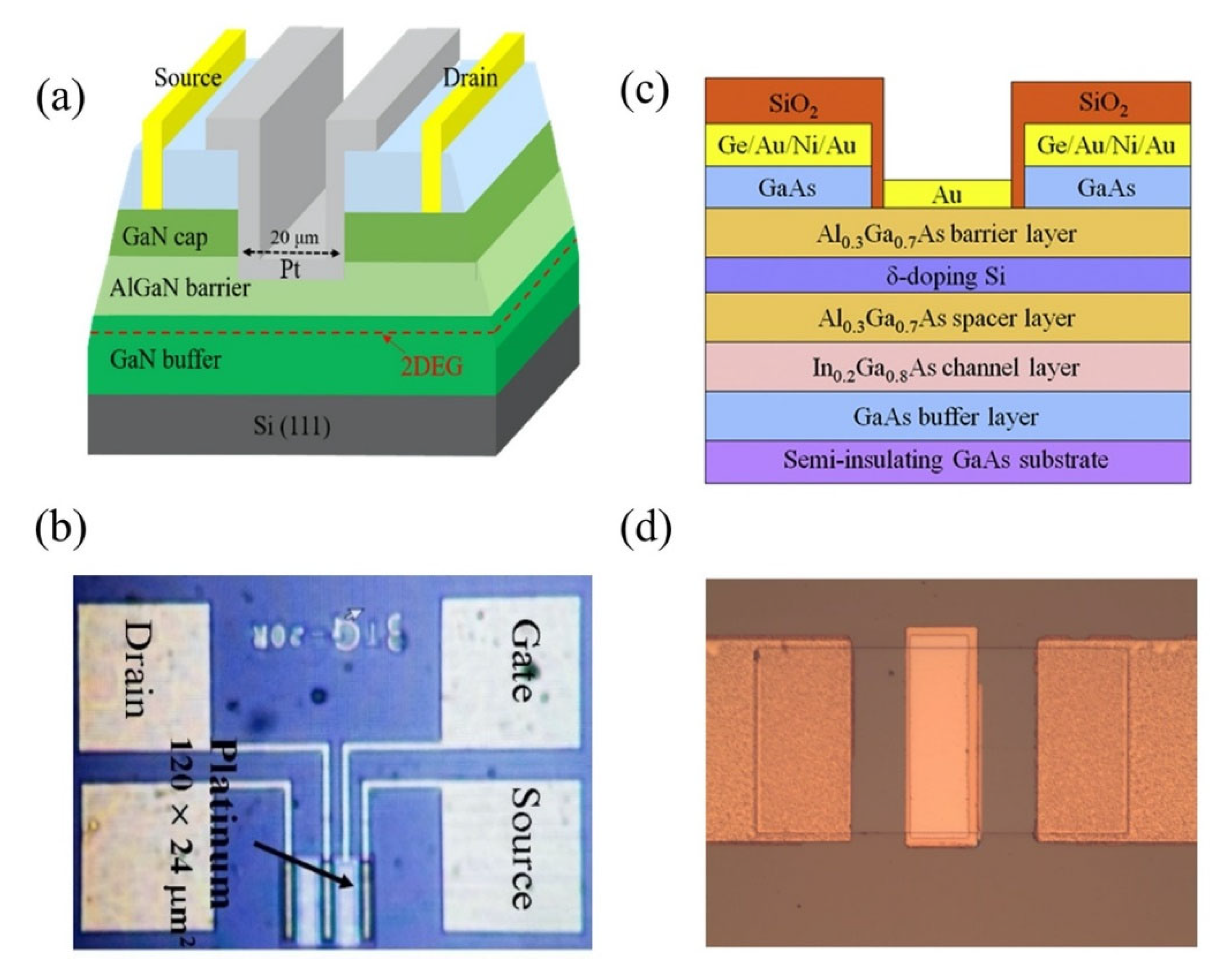
6. III-V Materials High Electron Mobility Transistor (HEMT)

Wide band-gap group III/V compounds, such as gallium nitride (GaN) and gallium arsenide (GaAs), are chemically stable semiconductors with high temperature/high power capability and high electron saturation velocity, which make them excellent materials for sensitive yet robust sensors. Aluminum gallium nitride (AlGaN) on a sapphire substrate is a great combination for the fabrication of high temperature sensors, as the thermal expansion coefficient of the sapphire substrate is in close proximity to Al2O3 or aluminum nitride (AlN) ceramides, which are often used as packaging materials for high temperature devices [170]. Both of the wide band-gap materials have been reported for the high thermal stability and long-term reliability, which is befitting for their use in extreme environments [171,172,173,174].
To date, the AlGaN/GaN high electron mobility transistor (HEMT) devices have been intensively studied for ion and biomolecule sensing applications such as gas sensors, chemical sensors and biosensors [175,176,177]. A typical HEMT epitaxial sensor device structure consists of a substrate (usually Si or sapphire), GaN buffer layer, AlGaN barrier layer, and GaN cap layer. Source and drain terminals were formed on the GaN cap layer, separated by a sensing area (gate). An example of a standard AlGaN/GaN HEMT three terminal device structure with a floating gate is shown in Figure 9a, and its top view microscopic image is in Figure 9b. Unlike conventional FETs in which channel conduction is governed by the majority carrier of holes or electrons (depends on the doping), HEMT’s conducting channel is fueled by two-dimensional electron gas (2DEG) arising from spontaneous piezoelectric polarization at the [0001] axis of the AlGaN/GaN heterostructure. Even though the 2DEG carrier mobility is incomparable to mobility of zero-bandgap graphene [178,179], HEMT has considerable potential as a highly sensitive sensor device with fast response time attributed to its higher 2DEG density and thinner barrier in the AlGaN/GaN layer, enabling direct detection of molecules or charged particles absorbed on top of its sensing area (gate) [180,181].
In recent years, some new sensing strategies for HMIs on AlGaN/GaN HEMT have been brought to light. For example, Nigam et al. and co-workers are currently one of the active groups working on AlGaN/GaN HEMT for the detection of heavy metal ions at the Indian Institute of Technology Jodhpur (India). The group of Nigam established an AlGaN/GaN HEMT functionalized with mercaptopropionic and glutathione (MPA-GSH) on the gate terminal for cadmium (Cd2+) ion identification [183]. GSH, a thiol-containing tripeptide, has been reported to be able to create binding with the Cd2+ ion [184,185]. This is supported by a published article, which reveals that the GSH-Cd binding forms a spherical shaped (GS)4Cd complex [186]. The MPA in this experiment served as a linkage between the Au covered terminal gate and glutathione. This sensor provided a LOD of 2.2685 nM and a sensitivity of 0.241 μA/ppb. Perhaps the most serious disadvantage of this method is the selectivity of the sensor. Even though the sensor demonstrated good selectivity towards Cd2+ ions, there were interferences from other heavy metal ions such as Cu2+, Hg2+ and Pb2+ in the selectivity analysis. It was reasonable to expect the sensor to respond to these HMIs because both Pb2+ and Hg2+ would form linear bonds with GSH, and the binding of Cu2+ by the MPA-GSH functionalized surface has been previously reported [187,188]. In the same year, Nigam and co-workers further reported a similar HEMT device functionalized with 2,5-Dimercapto-1,3,4-Thiadiazole (DMTD) for the detection of Pb2+ ions [189]. The detection of Pb2+ using DMTD ligand has previously been observed with different platforms [190,191]. Exploiting the similar idea, Nigam functionalized the DMTD ligands on the AlGaN/GaN HEMT gate terminal and observed its electrical response. The detection mechanism of this sensor was in a straightforward manner as the Pb2+ binds with the dangling thiol on the DMTD ligands, forming a Pb-DMTD complex. Due to this event, the density of 2DEG increased, which reflected the drain current increase. This investigation was more thorough than the previous one, as Nigam provided us with repeatability, recovery data and detection of Pb2+ in actual contaminated water, which is crucial to prove the practicality of the HEMT sensor in the real world. As disclosed by Nigam in his published article, the detection readings by his proposed HEMT DMTD-functionalized in as-prepared 48.826 nM Pb2+ ions electrolyte solution, tap water and lake water of Kaylana Lake (Jodhpur, India) are compatible with the readings of inductively coupled plasma mass spectroscopy (ICP-MS) that was used as a reference method in the investigation. The HEMT ion sensors achieved a sensitivity of 0.607 μA/ppb with a LOD of 86.87 pM. The sensor had rapid detection (response time approximately 4 s) and excellent repeatability, as only a small variation was observed when performing the sensing operations. Furthermore, the research group also demonstrated a new strategy for detecting mercury ions (Hg2+) using a molybdenum disulfide (MoS2) functionalized HEMT sensor [192], concerning the potential binding of the MoS2 with Hg2+ ions. The MoS2 consists of layers of one molybdenum sheet sandwiched between two sulfur sheets (S-Mo-S), which provide sulfide group layers as a site binding of Hg2+ ions. The authors reported sensor sensitivity of 0.64 μA/ppb with a detection limit of 57.43 pM and a response time of 1.8 s.
Another popular HEMT sensing strategy for HMI detection was integration with an ion-selective membrane (ISM). A sensing membrane is generally comprised of a primary ion (ionophore) and an ion exchanger (lipophilic salt) incorporated into a polymeric membrane [193,194]. The ionophores are employed to selectively bind with target ions, as convincingly reported in various conditions, for instance, laboratory-prepared chemical analyte, environmental sampling, blood or serum [195,196,197,198,199]. Chen et al. and co-workers have demonstrated the detection of Pb2+ with a metal ion selective membrane (metal-ISM) in combination with AlGaN/GaN HEMT [200]. In this work, the author focused more on the HEMT configuration instead of modification of the sensing area to improve the sensitivity of the HEMT sensor. The research group successfully demonstrated the ultra-sensitive Pb-ISHEMT (lead-ions selective high electron mobility transistor) beyond Nernst response. They confirmed that the sensitivity of the HEMT depended on the distance of the gate terminal from the HEMT channel and the applied gate potential. Figure 10a depicts the AlGaN/GaN HEMT test setup for evaluating sensor response with the variation of gate terminal distance and applied gate potential. Their findings show that the shorter the distance between the channel and the gate terminal, the higher the electric field available to modulate the carrier density of the HEMT channel, and the higher the current gain yielded. Moreover, the applied gate potential also plays an important role in the sensitivity of the Pb-ISHEMT sensor. The low applied gate potential yielded small gain currents; higher gate potentials were necessary to obtain larger gain currents. The experiment data of the effect of terminal gate distance and applied gate potential on the sensor response is presented in Figure 10b–g. With the optimized device configuration and gate potential, the Pb-ISHEMT sensor is capable of discriminating Pb2+ as low as 0.1 nM. In another published article, Chen experimentally confirmed that the sensitivity of an ISM-based HEMT sensor was not only reliant on the site binding theory (which observed the number of site binding metal ions depending on the surface porosity and roughness of the ISM), but instead, the linear HEMT device operation contributed to sensor sensitivity beyond Nernst response [201]. Chen mentioned the significant relationship between gate terminal distance and applied gate potential, which renders an ultra-sensitive HEMT sensor, and the authors reported the detection limits of Pb2+ and Hg2+ were 0.1 nM and 0.01 nM, respectively. In a different study, Hsieh et al. also worked on the Pb-ISHEMT sensor and proved Chen’s hypothesis [202]. Similarly, the distance between the gate terminal and the channel area, as well as the applied potential gate have been taken into account in order to reproduce beyond Nernst’s ultra-sensitive sensing performance. The sensor produced a good linear response towards Pb2+ over a wide dynamic range concentration of 0.1 nM to 10 µM with a LOD of between 0.1 nM and 0.01 nM. The results were in a good agreement with Chen’s theoretical and experimental data. Although reporting excellent sensor performance (sensitivity beyond Nernst response, low LOD and wide detection range), the article lacks important performance analysis such as selectivity performance in mixed solutions, detection in real samples and reproducibility data to substantiate the practicality of this sensing method in the real world.
Now we will turn to the mercury ion selective membrane (Hg-ISM) on AlGaN/GaN HEMT sensor for detection of Hg2+. Sukesan et al. constructed an array of Hg-ISHEMT sensors and connected them with a single FET that functioned as a switch to turn on each Hg-ISHEMT sensor [203]. The author reported an LOD and dynamic range of 0.1 pM and 0.1 pM–10 µM, respectively. The main driving force of this sensor, similar to the other ISM-based HEMT sensors, is based on the changes in dielectric capacitance (Cd) when the Hg2+ binds with the ionophore. The electrolyte/semiconductor surface potential dropped as the Hg2+ concentration increased, leading to an increment in current [204,205]. It is worth mentioning that the sensor was independent to pH and conductivity, which means that the sensor could provide an accurate reading in real time. The research group had examined the sensor performance in real tap water samples and the findings demonstrated that it had a similar response to the data in mercury test solutions. Moreover, the sensor had good specificity towards Hg2+ even in complex matrices. Later, they constructed Hg-ISHEMT sensors with a user interface that could estimate the concentration of Hg2+ in an unknown solution [206]. Interestingly, the response time of this sensor was observed to be further improved up to 5 min, compared to previous Hg-ISHEMT sensor response time (~10 min). As could be expected, the sensor achieved a sensitivity of −36 mV/log, which surpasses ideal Nernst slope (−29 mV/log) and detection limit of 0.1 pM. Moreover, the sensor sensitivity and detection limit were found to be autonomous in high concentrations of interfering ions, implying that no pre-treatment or re-calibration is required when testing in various solution test samples. Integration of Hg-ISHEMT with the user interface expanded the possibility for commercialization. Other electrical detection of heavy metal ions on AlGaN/GaN HEMT sensors is summarized in Table 5.
As reported by several papers mentioned above, AlGaN/GaN HEMT is a popular platform for HMIs detection. On the other hand, AlGaAs/GaAs HEMT has been rarely reported as a biosensor in recent years, let alone for HMIs detection. In comparison to the AlGaAs/GaAs HEMT device, the AlGaN/GaN HEMT possesses a larger sheet carrier concentration at the surface owing to a larger piezoelectric effect, which consequently contributes to its popularity as a highly sensitive biosensor [207]. In the past ten years, there has only been one study published on HMIs detection using an AlGaAs/InGaAs HEMT sensor. Wang et al. conjugated one-end thiol modified ssDNA on the Au gate electrode of the AlGaAs/InGaAs HEMT device for specific detection of mercury (II) ions [182]. The AlGaAs/InGaAs HEMT structure and its top view photomicrograph in Wang’s work are shown in Figure 9c,d, respectively. This HEMT sensor sensing mechanism relies on the coordination interaction of Hg2+ with bis-thymine. The Hg2+ presence at the gate electrode changed the surface charges of the HEMT, resulting in the change of 2DEG concentration. The AlGaAs/InGaAs HEMT sensor successfully detected Hg2+ ions as low as 10 nM. This observation provides conclusive evidence that the AlGaAs/GaAs HEMT structure is suited for bio- and chemical sensing applications. However, the only drawback to this AlGaAs/InGaAs HEMT sensor is the complexity of the heteroepitaxial layer growth.

7. Transition Metal Dichalcogenides (TMDs)-Based FETs

Graphene has successfully gained popularity as an electrode material for many applications at nanoscale sizes ranging from electronic devices to sensing and actuation. However, with zero bandgap characteristic, the application of graphene as a nanoelectronic device is limited. This graphene drawback has motivated the search for a more suitable material. Transition metal dichalcogenides (TMDs) materials are a promising candidate for nanoelectronics applications owing to their direct and tunable small bandgap properties. Being physically similar to graphene, the TMDs semiconductor materials have a large surface area and high carrier mobility that is well-suited for sensing applications [213]. Moreover, TMDs have become an attractive material for FET applications as they offer gate-tunable conductance owing to high current on/off ratios [214]. This attractive factor of high current on/off ratios plays an important role in sensor response time. The higher the current on/off ratios, the faster the response speed of the sensor [215].
The TMD materials are a combination of transition metal elements with chalcogen atoms in which their structure can be defined as X-M-X or MX2 (M represents the metal transition while X represents the chalcogen atoms). Simply put, the TMDs are made up of a plane of transition metal that is sandwiched between two layers of chalcogen atoms. An illustration of TMDs’ atomic structure is given in Figure 11. The transition metal candidates include molybdenum (Mo), tungsten (W), titanium (Ti), zirconium (Zr) or Hafnium (Hf), whereas the flexibility of chalcogen element choice is rather limited. Three elements that are often found in the literature are sulfur (S), selenide (Se) and tellurium (Te). Since the seminal work by Dickinson and Pauling synthesized molybdenum disulfide (MoS2) in 1923, the S has been a popular choice of chalcogen atom of TMD material and has shown promise in evolution [216]. Se has been recently gaining popularity as an element in TMDs due to its high electrical conductivity, while Te is an expensive option to synthesize TMDs material; consequently, its potential is only suited for specific applications, making it the least popular option in the family of chalcogens. The application of TMDs as sensing and biosensing materials, began in 2013, which primarily focused on electrochemical fluorescence sensing. Therefore, the TMD material for sensing applications is still considered to be in its infancy stage. So far, only MoS2 and WS2 materials have been reported as FET materials for heavy metal ion detection. In the near future, we can expect the other TMD compounds to be exploited for FET sensing applications.
MoS2 is the most intensely studied TMD material due to its synthesis maturity technology, stability and ruggedness as well as high availability [218]. The TMDs-based FET, pioneered by Radisavljevic et al. in 2011 [219] using MoS2 material as a conductive channel of a FET, paved the way for the development of the TMDs-based FET sensor. In recent years, increasing interest has been paid to TMDs materials as an FET platform for HMI detection. Zhou et al. demonstrated a MoS2-based FET for the detection of Hg2+ using DNA-AuNPs as probes to capture the ions [220]. The changes in MoS2 conductivity upon detection of Hg2+ can be explained by electron transfer from Au NPs to MoS2 film, resulting in a decreasing concentration of holes, which consequently induces its conductivity. This MoS2/DNA/Au-FET sensor demonstrated rapid response within 1–2 s with an ultralow detection limit of 0.1 nM. Notably, this sensor’s response time was faster than that of the electrochemical sensor, which takes 30 s to 180 s to respond [221,222]. One plausible explanation for the ultrasensitivity of this sensing strategy was attributed to MoS2. To verify this hypothesis, the research groups carried out a systematic series of experiments to investigate the relationship between sensing performance and different MoS2 thin film thickness, carrier mobility, and size of the bandgap (of MoS2). Their results indicated that a thinner MoS2 film with greater carrier mobility, and a wider band gap, would result in increased sensitivity (lower detection limit). Detection of Hg2+ on the bare MoS2 thin films has also been reported. Jiang et al. have investigated the performance of the MoS2-FET sensor in the detection of Hg2+ without any sensing probe [223]. In this study, Jiang et al. investigated the absorption of Hg2+ on a few-layers of the MoS2-FET channel. The findings of their studies revealed that, without Hg2+ presence, the MoS2-FET current-voltage curve reflected an n-type semiconductor characteristic. However, upon introducing Hg2+ to the FET channel, the drain current decreased. Furthermore, the authors claimed that as the Hg2+ concentrations increased, the MoS2-FET current-voltage characteristics progressively changed to p-type. This phenomenon suggests that the coordination of Hg2+ with the S2- ligands on the surface of MoS2 leads to a p-type doping effect due to partial electron transfer from MoS2 to Hg2+. On this basis, they further investigated the p-type doping effect of Hg2+ on the MoS2 surface using photoluminescence spectroscopy. The result of photoluminescence studies were in line with the FET measurement. This sensing strategy yielded a detection limit as low as 30 pM.
Li et al. and colleagues demonstrated MoS2-FET with different metal contacts for detection of arsenic [224]. They utilized an ionophore thin film to selectively permeate arsenic dioxide (AsO2-) onto the MoS2 FET channel and serve as a negative gate voltage. When the AsO2- ions bound to the MoS2 surface, the electrons in the bulk were repelled (pristine MoS2 is an n-type semiconductor in nature), resulting in lower MoS2 conductivity. The change in conductance was expected due to the absorption of the target molecules on the MoS2 surface [225]. A schematic diagram of MoS2-FET with an ionophore thin film and its top view optical image are shown in Figure 12a,b, respectively. Further, the research group investigated the Schottky barrier (SB) height at the metal contacts of the source/drain in relation to the sensitivity of the MoS2-FET sensor in an aqueous environment, inspired by the work of Liu et al. who investigated the sensing performance of the MoS2 gas sensor with a different height of Schottky barrier [226]. The sensitivity of the MoS2-FET towards AsO2 was examined using three different metal contact work functions (Φ), namely: platinum (ΦPt = 5.9 eV), Nickel (ΦNi = 5.0 eV) and titanium (ΦTi = 4.3 eV). The relationship of Schottky barrier height with the work function of the metal contact can be described as ΦSB = Φ − Ψ, where Ψ is the MoS2 electron affinity constant. Therefore, the Schottky barrier height of MoS2 FET can be placed in the order of Ti < Ni < Pt according to their work function. Experimental results in Figure 12c show that the shortest Schottky barrier height (titanium) demonstrated the best sensitivity as the FET device showed the biggest resistive change when operating in an aqueous environment. Beyond that, the MoS2 FET with a shorter Schottky barrier height determined better device conductivity. Figure 12d,e present a comparison of FET drain current performance with titanium and platinum metal contacts. From the results, the FET with titanium metal contacts has better conductivity (higher drain current) compared to the FET with platinum metal contacts. This study has shown that the reduction of Schottky barrier height has conclusively improved the MoS2 sensor performance. This sensor was reported to be able to detect As3+ as low as 1.3348 nM with excellent selectivity towards AsO2, owing to the ionophore film to filter out other interference ions. Recently, Li and his research group further explored their interest in the MoS2-FET sensor by investigating the influence of tensile strain on the sensing performance of flexible MoS2-FET ion sensors [227]. Strain is a critical parameter for flexible/stretchable chemical devices. Several studies have concluded that the strain could create a piezoresistive effect on flexible MoS2 material, which the resistivity of the material changes due to band structure changes during mechanical deformation [228,229,230]. The results of the studies showed that the drain current of the FET increased as the strain was increased from −0.17% to 0.17%, suggesting the tensile/compression strain promoted the band gap reduction and consequently enhanced the electrical conductivity. This MoS2-FET ion sensor behavior under strain conditions shows excellent agreement with the experimental results of a recent study by John et al. [231]. For sensing studies, the MoS2-FET ion sensor was fabricated in an array and functionalized with four different ionophores (sodium ionophore, cadmium ionophore, mercury ionophore and lead ionophore). The resulting sensor exhibited merit for simultaneous detection with exceptional selectivity towards sodium, cadmium, mercury and lead ions. Under a strain condition, the MoS2-FET ion sensor was able to detect Cd2+ as low as 5 ng/mL with a response time of 8 s. In addition, the sensor demonstrated promising potential in real-life applications as it successfully monitored Hg2+ ions in tap water and Na2+ ions in human sweat samples. Next, MoS2 material was also reported in the fabrication of the chemiresistor ion sensor. A recent published study by Bazylewski et al. [232] demonstrated that MoS2-chemiresistor functionalized with L-cysteine (Cys) exclusively for the detection of Cd2+. The sensor devices were reported to be able to detect Cd2+ ions in the range of 8.896 nM–4.448 µM at neutral pH with a response time of ~1 s. The studies also explored the effect of pH on the chemiresistor performance. The pH-dependent experiment was carried out in buffered solutions pH 3–10. The results revealed that the sensor struggled with selectivity at lowest pH (<pH 5) and highest pH (>pH 9), limiting the detection window to pH 5–9. It is worth noting that the detection in pH 6–7 demonstrated high selectivity towards Cd2+ despite the presence of other interference metal ions with similar hydrodynamic radii. The resistivity of the chemiresistive sensor also increased by 20 times in water that contained a 44.48 nM concentration of Cd2+ ions.
A three-dimensional (3-D) flower-like MoS2 nanostructure for HMI detection has also been reported. As shown in Figure 13a,b, the 3-D flower-like MoS2 is made up of a large quantity of MoS2 microspheres, each of which is built from nanosheets that tie together at the center to form a 3-D flower-like structure. The unique structure of MoS2 flower-like has attracted a great deal of attention in nano sensor applications. It has the major advantage of maximizing the performance of the sensor, owing to its high surface area, which provides large numbers of potential reaction sites. An et al. developed a 3-D MoS2-based FET aptasensor to detect Arsenic (III) in real river water [233]. In this work, the sensor was fabricated as an interdigitated microelectrodes array (IDA) on a glass substrate. The surface of the glass substrate was treated with 3-aminopropyltrimethoxysilane (APS), to provide amino functional groups as anchors to carboxylic polypyrrole (CPPy)-coated flower-like MoS2 nanospheres (CFMNSs). Finally, arsenic binding aptamer (Ars-3) was immobilized on top of the CFMNSs as a probe to recognize As3+. The resulting sensor could detect As3+ as low as 1 pM, and the sensor response in less than 1 s. The response time of the 3-D flower-like MoS2 FET aptasensor was faster compared to the 3-D flower-like MoS2 functionalized AlGaN/GaN HEMT reported by Nigam et al. which responded on a time scale of 1.8 s [192]. Moreover, the 3-D flower-like MoS2 FET aptasensor had excellent selectivity towards As3+ in real river water samples. The extraordinary performance of this sensor might be contributed by the CPPy coating layer, which enhances the conductivity of the MoS2 and the number of functional groups.
Besides MoS2, tungsten dichalcogenides are also receiving attention from researchers for their application in HMI detection. Neog et al. first described the potential of WS2 as a chemiresistor sensor for the detection of HMIs [235]. The result of his studies showed that the I-V characteristic of the untreated (bare) WS2-chemiresistor was linear in the voltage range of −9 V to 9 V and the maximum current obtained was in nA scale. The linear I-V characteristic reflects WS2 ohmic behavior, where the current flow is proportional to the direct voltage across the chemiresistive device. However, with the presence of 17.906 µM of Fe3+ and 16.968 µM Co2+ in the test solutions, the I-V characteristics of the devices were abruptly changed and the current was raised to µA range. Evidently, the WS2 chemiresistor device was no longer following Ohmic’s law. One unanticipated finding was that the reversible properties of WS2 nanosheet. When all the ions were removed from the WS2 surface, the chemiresistor restored the original electrical behavior. This finding opens the opportunity for the WS2 chemiresistor as a reusable electrical detection for heavy metal sensors. Despite this promising result, repeatability and reproducibility studies of the WS2 chemiresistor devices are recommended to determine its stability and reliability. The LOD of this WS2 chemiresistor was 30 µL to change its electrical behavior to atypical (non-ohmic). In another study, Neog et al. further explored the potential of the WS2 chemiresistor by detecting different HMIs [236]. The WS2 chemiresistor exhibited resistance changes towards eight different ions (As3+, Ni2+, Cu2+, Sn2+, Se4+, Hg2+, Pb2+ and Zn2+), but the most prominent resistance changes of the WS2 chemiresistor occurred in the presence of Zn2+. Later, the Zn2+ content present in the solution was quantified by using the peak and valley difference method. The WS2 chemiresistor showed high selectivity to Zn2+ ions, with a LOD of 14.375 ± 0.7646 nM, and a sensitivity of 0.63 ± 0.05 µA/ppb.

8. Other FETs

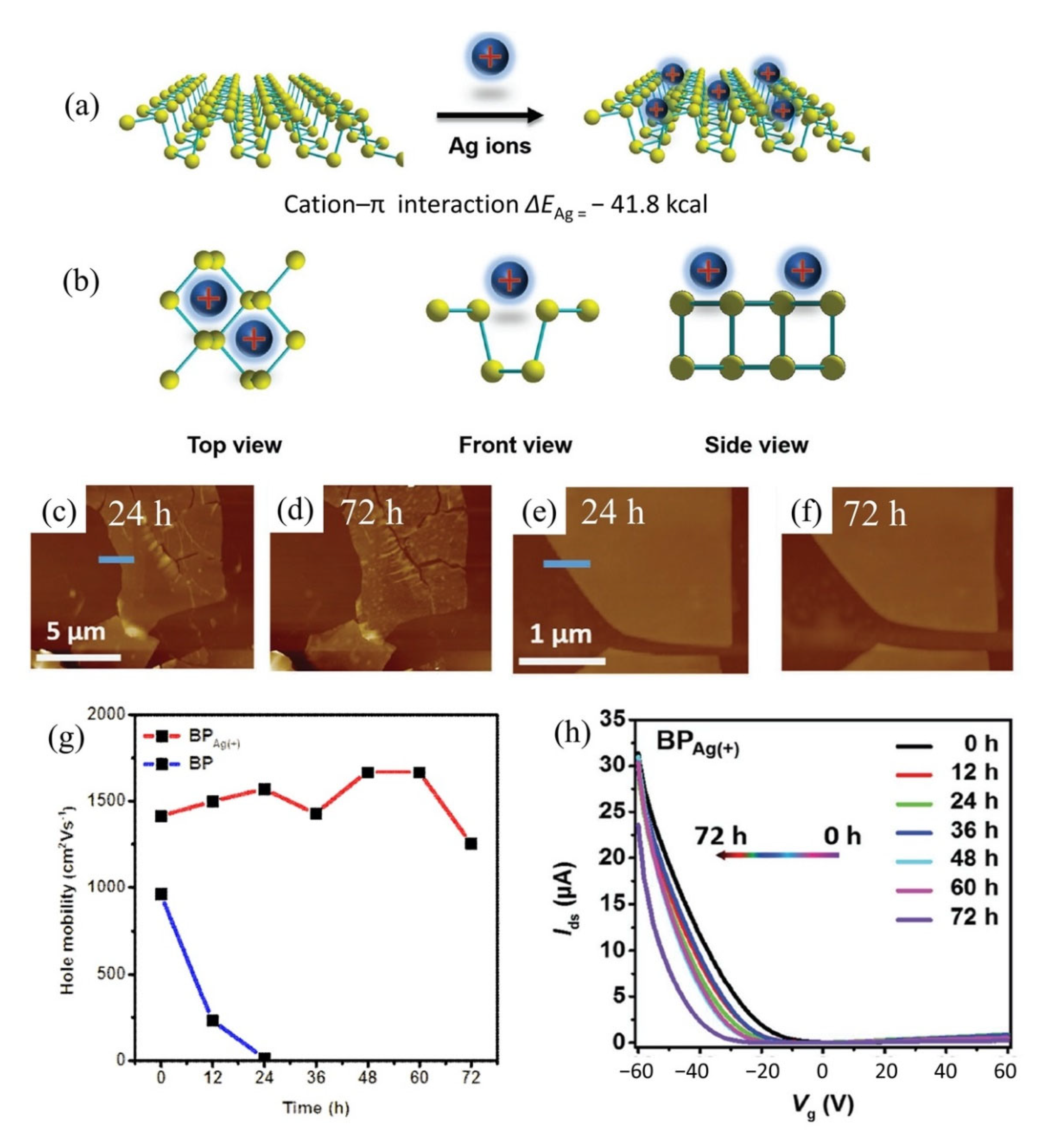
8.1. Black Phosphorus FET

Black phosphorus (BP) is one of the members of a two-dimensional (2D) family of materials that possess unique properties, including biocompatibility, in-vivo biodegradability, large surface-to-volume ratio and tunable bandgap [237]. BP’s electronic properties are superior to those of other semiconductor materials. BPFET is reported to have higher carrier mobility (1000 cm2.V−1.s−1) than TMD-FET [238]. Moreover, the BP current on/off ratio (103–105) is larger than published graphene transistors [239,240]. On top of that, BP’s molecule absorption energies are larger than those of graphene and MoS2 [241]. Despite these remarkable properties, BP appears to be unstable in ambient conditions [242,243,244]. As a result, it makes BP less attractive for practical application. In recent years, many researchers have attempted to improve BP stability, thereby enabling its potential for biosensor application. Firstly, the implementation of passivation has been proven as a possible approach to stabilize the black phosphorus in the air. Upon passivation, different materials have been suggested to be incorporated onto the BPFET sensing channel, aiming to improve stability. For example, Li et al. reported [245] the use of lead ionophore as passivation on their BPFET. The specified ionophore not only improves the stability of BP, but it also serves as a sensing element to detect a specified ion. An ionophore is a coating film that can discard undesired ions from the environment and only allow specified ions to permeate through it. In this case, only Pb2+ was expected to reach the BP sensing area while other ions are filtered through the ionophore film. The Pb2+ that permeates through the ionophore film functions as a positive gate voltage and, consequently, repels the positively charged holes in the channel area, leading to conductance decrease. The BPFET sensor shows an LOD of 4.826 nM. Another good passivation suggested to promote BP stability is SiO2, Al2O3, aryl diazonium, titanium sulfonate ligands and PEG [246,247].
Dithiothreitol (DTT) conjugated with AuNPs was functionalized on the BPFET for the detection of As3+ in water [248]. In addition to functioning as an As3+ recognition element, DTT is also well known as a reducing agent of As5+ to As3+ [249,250,251], suggesting that the proposed BPFET sensor would be able to detect As5+ as well. The detection of this sensor was based on the simple interaction of thiol-containing ligands at DTT with As3+ [4]. A detection limit of 1 nM was obtained, and this ultrarapid sensor demonstrated a fast response of 1–2 s. Since thiol is a versatile probe for many metal ions, the selectivity of the sensor was a bit complicated. Hence, ethylenediaminetetraacetate (EDTA) was added into the test solution during selectivity analysis to suppress the activities of other metal ions [252], resulting in a significantly improved specificity of the sensor towards As3+.
The direct detection of metal ions on the BP without any surface functionalization or passivation has also been reported. Wang et al. described a simple approach for electrical detection of Ag+ using black phosphorus FET (BPFET) [253]. The sensing mechanism of this sensor relies on the direct absorption of Ag+ on the BPFET sensing surface. The HMIs Ag+ interacts directly with the conjugated π bond derived by the lone pairs of phosphorus atom in the surface layer as illustrated in Figure 14a. There are three different possible views of the Ag+ absorption on the BP layer shown in Figure 14b. This sensor could detect Ag+ at a detection limit of 10−10 mol/L (92.7 pM), which was lower than the safe limit of Ag+ in drinking water set by the World Health Organization (0.927 µM). The response of this sensor was averaged at 60 s for each sample. While the sensor yielded good sensitivity towards single ion detection of Ag+, the selectivity of this BPFET sensor in multi-ions electrolyte was unknown. Evidence shows that the conjugated π bond on the phosphorus layer can also bind with other metal ions (Mg2+, Fe3+ and Hg2+) [254]. Therefore, an extended study to determine the sensor selectivity towards Ag+ in complex matrices is needed. It is also worth pointing out that the absorption of Ag+ could stabilize the BP layer. Guo et al. carried out a series of experiments to investigate the stability of BP material with Ag+ absorption [255]. Figure 14c–f compares the atmospheric stability of bare BP and BPAg+ from day 1 to day 3, consecutively. It was observed that there were bubbles formed on bare BP after 24 h exposed to the atmosphere, and after day 3, the bubbles increased in size. Whereas in the case of BPAg+, the surface layer was preserved and showed no obvious bubble formation. The hole mobility of BPAg+ was also stable (1500 cm2Vs−1) at least up to 72 h when compared to bare BP, which degraded to 0 cm2Vs−1 after 24 h, as demonstrated in Figure 14g. The drain current of a BPAg+-FET was degraded by 28% only after 72 h (Figure 14h). These multiple analyses revealed that the absorption of Ag+ on the BP surface layer promotes the stability of BP materials.
Chang et al. and colleagues introduced a semi-quantitative FET model to estimate and describe the direct absorption metal ion density, LOD, and sensing mechanism on the FET channel surface [256]. In this work, the research group developed a BP nanosheet FET sensor to validate the FET model. Based on ion concentration and intrinsic FET material properties, such as band gap and carrier density, they developed a statistical thermodynamics model that will be able to predict the LOD of a FET sensor. On top of that, the semi-quantitative model could also describe the sensing mechanism of the FET by relying on the relative size of the Debye length and the distance between absorbed ions. From the findings, they concluded the detection mechanism at low ion adsorption density was dominated by the charge transfer effect. While at high ion adsorption density, the detection of metal ions was predicted to be controlled by a gating effect. Application of the semi-quantitative FET model was evaluated in Na+, Mg2+, Zn2+, Cd2+, Pb2+ and Hg2+ solutions. Among the other metal ions, Hg2+ was found to be more responsive with this BP-FET sensor. The LOD of Hg2+ is predicted to be 0.1 nM in tap water and 0.1 fM in deionized water. The implication of this study raises the possibility that the BP-FET can be used as a probe-free detection sensor in a wide range of ion sensing applications.

8.2. Organic Field-Effect Transistor (OFET)

The organic field-effect transistor (OFET) belongs to the thin film transistor (TFT) family, which employs organic semiconductors (OSCs) as an active electrode. The OSCs are flexible, unbreakable, lightweight and have a low power consumption, which makes them an ideal electrode for TFT applications [257]. Many mistake OFET as an MOSFET. However, OFET is different than MOSFET in several ways. First, the principal operation of the OFET is rather straightforward compared to the MOSFET. OFET operates under accumulation mode [258], for which its conductance is directly controlled by the gate voltage applied. Secondly, the mobility of OSC is often lower (10−1~10−2 cm2/Vs−1) than that of crystalline silicon. OFET has been extensively used for biosensors, but only a few studies have reported on OFETs for heavy metal detection. Herein, we will discuss some of the recently developed OFETs for determination of HMIs.
Minami et al. developed an OFET sensor for detection of Hg2+ in sea water [259]. In this sensor, L-cysteine, which can selectively bind to Hg2+ ions through an Hg–S bond, was conjugated onto an extended-gate gold electrode as a recognition element. The main driving force of this sensor was laid on the interaction of Hg2+ with cysteine to form an Hg–Cys complex, which consequently, changed the OFET conductance. Even though the OFET sensor confirmed its sensitivity and provides a detection limit (LOD) of 154.54 nM, the performance of this sensor did not meet the expectations for measurement in real sea water samples. This is because the mercury level in the sea water sample is comparatively low (below 0.997 nM). Therefore, a sensor with better LOD is anticipated. It is worth mentioning here that the OFET sensor exhibits good selectivity towards Hg2+ ions, which is attributed to the high binding affinity of thiols in the L-cysteine structure for Hg2+. In another approach, an artificial receptor was used at the gate electrode of OFET to detect Hg2+ [260]. The extended-gate gold electrode was functionalized with thiolated DPA self-assembled monolayer (SAM) to probe Hg2+ in a prepared solution with the interference of Na+. Similar to the work described previously, the detection mechanism of the sensor was also based on the affinity binding of thiols with Hg2+. This method has achieved a detection limit of 49.35 nM, which is lower or comparable to the other sensors [261,262,263]. Further, the sensor was tested in a multi-ion electrolyte to evaluate its selectivity towards Hg2+. The findings reported that all the other interference ions’ responses are almost negligible, suggesting the sensor’s excellent selectivity. In this work, the reusability of the sensor has also been investigated. Surprisingly, the sensors exhibit no degradation after a few washes with an EDTA solution. In practical application, the reusability of a sensor is important for cost effectiveness.
Knopfmacher et al. used a high mobility polyisoindigo-based polymer with siloxane-containing solubilizing chains (PII2T-Si) as an active semiconductor material to efficiently detect Hg2+ in the marine environment [264]. In order to selectively detect Hg2+, the PII2T-Si surface was functionalized with DNA conjugated gold nanoparticles (AuNPs) prior to sensing in sea water. The DNA-AuNPs probes formed a hairpin structure upon binding with the Hg2+. This conformational change resulted in a negatively charged increase on the OFET’s surface, consequently resulting in hole carrier accumulation in the organic semiconductor. This sensing method allowed for an Hg2+ detection limit down to 10 μM. The most striking finding to emerge from this experiment is that the OFET sensor has the ability to detect Hg2+ in a high concentration of salt in sea water (~600 mM) without any sample pre-treatment. To the best of our knowledge, this is the first selective sensing strategy using polymer OFET in the marine environment. In practice, the OFET sensor easily deteriorates when in contact with aqueous media alongside high operating voltages. The instability of the organic semiconductor has restricted the application of OFET as a reproducible and reliable chemical or biological sensor in the real world. To overcome this shortcoming in OFET, recently, Sayyad et al. reported the incorporation of carbon nanomaterial in organic semiconductor [265]. In the analysis, reduced graphene oxide (rGO) was incorporated into the PEDOT: PSS to form a new hybrid material, the PEDOT: PSS/rGO nanocomposite, which has improved structural, morphological and electrical properties. Later, the PEDOT: PSS/rGO was utilized to fabricate an OFET for detection of Hg2+. PEDOT: PSS/rGO OFET exhibited a good linear response towards mercury ions over a wide range of concentrations, from 1 nM to 60 nM, with a LOD of 2.4 nM. In another study, Hg2+ detection was realized using polyaniline nanowires (PANI NWs) OFET functionalized with EDTA [266]. In the presence of Hg2+, the drain current was observed to be increased, indicating Hg-EDTA complex formation on the OFET surface. The OFET sensor sensitivity of 0.766 mA/ppb was obtained and the LOD of the sensor was down to 0.7214 nM.
In order to detect copper (II) ions in water, Sasaki et al. [267] proposed an unlabeled extended-gate OFET sensor decorated with nitrilotriacetic acid (NTA) monolayer. This simple approach achieved an LOD of 1.5106 µM for Cu2+ detection. The sensing mechanism of this sensor relies on the interaction of Cu2+ with NTA, which has induced a decrease in FET channel conductance. In selectivity analysis, the sensor showed no response to the other metal ions, however there had been a little response to the presence of Ni2+. The Ni2+ might be competing with Cu2+ to electrostatically bind with the receptor. Thus, the use of a masking agent to seclude the Ni2+ prior to sensing is essential to improve the sensitivity and selectivity of the sensor. In a related study, Ramesh et al. demonstrated the determination of Cu2+ using a pentacene/Schiff base pyrene derivative that would change to star-shaped in the presence of Cu2+ [268]. Figure 15a,b illustrates the before and after detection of Cu2+ on OFET functionalized with pyrene derivatives, respectively. The mechanism of the sensor mainly relies on the formation of excimer pyrene (P−P*). Chemically, upon the presence of Cu2+, monomer OH- functional group was deprotonated to let the hetero atoms (O and N) and Cu2+ (chelator) engage in the formation of an excimer P−P* [269], thereby leading to the VTH and off current change. At the same time, the non-uniform pyrene thick rods on the OFET surface were broken into pieces and re-assembled into star shapes, as shown by the AFM image in Figure 15c. The OFET sensor demonstrated exceptionally good selectivity and sensitivity towards copper ions as the VTH and off current changed significantly in the presence of Cu2+ as seen in Figure 15d,e, respectively. This approach yielded sensitivity in the range of 20–350 μM and a LOD of 50 μM.

8.3. Inorganic-Based FETs

Among the metal oxides (inorganic semiconductors), zinc (Zn), indium (In), gallium (Ga) and tin (Sn) are the most studied materials for electronic applications because they are non-toxic [270]. Binary compounds of these elements, such as SnO2, ZnO, In2O3 and Ga2O3, have been employed as an active layer of TFTs [271,272,273,274]. Contrary to organic semiconductors, amorphous metal oxide or inorganic semiconductor materials have not received much attention in the sensor field, primarily due to their mechanical instability and mediocre performance compared to vacuum-processed inorganic devices [275,276]. Additionally, the oxide metal formation by the sol–gel technique requires a high processing temperature in order to obtain optimal electrical performance [277]. Metal oxide binary compounds have also been reported to have poor device performance (e.g., high electrical resistivity, unstable and low on-off ratio) [278], limiting their use in electronic device applications. Despite these drawbacks, metal oxide semiconductors do have notable advantages for sensing transducers, such as straightforward device fabrication, large surface area and fast deposition [279]. Therefore, many researchers have focused on these advantages for next-generation sensing devices. The present studies show that the metal oxides can still be feasible in sensing applications. We follow with a review the recent work on the metal oxides TFT specifically for heavy metal detection.
Alqahtani et al. investigated SnO2 water-gated TFT (SnO2 WGTFT) to detect Pb2+ and Cu2+ [280]. In this investigation, the research group has employed natural zeolite clinoptilolite ionophore as a sensing element in a polyvinylchloride (PVC) membrane. The configuration of the SnO2 WGTFT sensor device was described as a twin-pool gating setup, which consists of two pools of tap water separated by a PVC based ion-selective membrane, inspired by the classical potentiometric ion sensor. The tap water at the bottom pool was as drawn (without added ions and functioning as a reference solution) and directly in contact with the SnO2 substrate, while the latter was added with a known concentration of lead or copper ions (target analytes). A tungsten (W) needle was immersed in the latter pool, acting as a reference electrode. For a proper understanding of this sensor configuration, we illustrated a cross-section of this TFT sensor in Figure 16. The sensing mechanism of the TFT sensor relies on the ion movement on the target/membrane interface, resulting in a potential difference between target analytes and reference solution, observed with the threshold voltage, VTH shift. If the ion activities in the target analytes match those in the reference electrolyte, no VTH shift will be observed. This potentiometric-TFT ion sensor offers several advantages over typical TFT. For example, it can be manipulated to sense various ions by introducing an appropriate sensing membrane. Clearly, this type of sensor does not require direct modification to the semiconductor TFT channel, which provides stability for the overall device. Moreover, since the TFT semiconductor channel does not involve any probe binding (e.g., aptamer or proteins), the potentiometric-TFT sensor allows for a simple recovery process. The sensitivity and detection limit of the TFT sensor can also be tuned by altering the properties of the sensing membrane [281]. This SNO2 WGTFT sensing strategy provided Pb2+ and Cu2+ detection with LOD of 0.9 nM and 14 nM, respectively. In another study of metal oxide based TFT for HMIs detection, Kim et al. utilized nanoglobules of ZnO/GO and ZnO/rGO for the development of multiple ion field-effect transistors (MI-FETs) sensor [282]. The sensitivity of the MI-FETs sensor was examined for a variety of ions, including Ni2+, Co2+, Cu2+, Cr3+, Fe2+ and Bi2+. However, the ZnO/GO and ZnO/rGO MI-FET only showed significant response towards Cr3+ and Cu2 for which the sensitivity was 49.28 mA µM−1·cm−2 and 185.32 mA µM−1·cm−2, respectively. The MI-FET nanoglobules ZnO/GO channel exhibited an LOD of 7.05 µM while the LOD of nanoglobules ZnO/rGO MI-FET was 14.9 µM.
Indium (III) oxide (In2O3) and tin-doped indium oxide (ITO) have been addressed as an interested field recently [283,284,285]. Both the In2O3 and ITO materials exhibit metal-like behaviors. ITO belongs to the transparent conducting oxides (TCOs). Its carrier density can be up to 1021 cm−3 and resistivity can be down to 10−5 Ω cm. The use of In2O3 and ITO as HMI FET sensors has not been investigated. However, ITO has been reported to be used in the OFET structure as a supporting material to detect Hg2+ [286]. ITO thin film served as the bottom channel material to increase the channel carrier concentration and maximum channel current of the OFET sensor. Cong et al. earlier used ITO in their TFT structure for similar purposes [287]. The OFET sensor in this work was conjugated with pyrene, which has been widely employed as recognition probes for mercury (II) ions owing to strong affinity binding between pyrene-thiol functional groups towards Hg2+. The LOD of the TFT sensor was observed to be 25 µM in tap, drinking and sea water samples. The response of the TFT sensor was found to be linear with the concentration of Hg2+ in the range of 1 mM to 0.01 µM.
A recent study by Qu et al. has unveiled the potential of ITO and In2O3 as transducer material for electrolyte gate FET [288]. In this study, Qu et al. developed ITO and In2O3 electrolyte gated FETs (Figure 17a) and studied their electrical behavior. In2O3 thin film and ITO (with Sn doping of 1.7% and 10%) have demonstrated FET current-voltage characteristics, as shown in Figure 17b–d. We noticed that the FET behavior was evaluated under different temperatures, suggesting the robustness of these thin films as FET sensor materials. Furthermore, Qu’s study also discussed the ligand binding options on these thin films, which established our understanding of ITO and In2O3 surface functionalization. According to Qu, hard acids such as acetic acid are more suitable as ligands for these indium based oxide materials compared to thiols because the hard base nature of In3+ has poor affinity towards thiol ligands [289]. These findings not only extend the application of ITO and In2O3 as potential materials for FET devices, but also stimulate new opportunities for investigating these thin films for HMIs detection.

9. Conclusions and Future Scopes

In the past 10 years, a significant effort has been made to realize high sensitivity and specificity of electrical detection for heavy metal ions (HMIs). Nanomaterial silicon, CNT, graphene, AlGaN/GaN, TMD, black phosphorus, organic and inorganic semiconductors have been demonstrated as a powerful and effective sensing platform for HMI detection in combination with different types of molecular recognition. At the same time, many detection strategies were explored on the FET platform to achieve ultrasensitive sensor performance. The lowest LOD obtained so far is as low as 10 fM, and most of the detection was achieved in real time. Within the past 10 years, graphene FET and AlGaN/GaN HEMT have rapidly shown an advancement in monitoring HMIs compared to other semiconductor nanomaterials. We believe that because of graphene’s versatility and availability, it has emerged as the preferred transducer material for FET sensors. Contrary to the AlGaN/GaN material, even though it is slightly expensive and has a complex fabrication process compared to the other materials, it nevertheless offers high sensitivity detection in high concentration solutions, and it has been proven that AlGaN/GaN HEMT can operate beyond the Debye length in physiological solutions (i.e., human serum).
Despite this progress, the FET sensing method still has room for improvement. It offers a satisfied sensing platform for monitoring different kinds of HMIs. However, there are a few concerns that need to be addressed before an FET-based sensor can be realized commercially for HMI detection. So far, the majority of the works reviewed here have only been demonstrated as proof-of-concept sensors capable of detecting HMIs in prepared solutions in laboratories. Only a minor study shows FET practicality of HMIs sensor in real samples. De facto, it remains a challenge to implement FET sensors to monitor HMIs in real world samples. First, real world samples such as industrial water waste, blood, tap or river water and soils are complex matrices that contain unknown elements or ion species. Unknown ions could interfere with the sensor signal. Therefore, the accuracy of the FET sensors is debatable in this case. Multiple sensing HMIs using FET array sensors might be an effective solution to address this problem. Secondly, nearly all the studies in laboratories reported the performance of the FET sensor testing in single ion HMIs buffer solutions. But in reality, the HMIs exist as metal-organic complexes. Prior to sensing with the FET sensor, real HMI analyte samples are often pre-treated (extraction, separation, dilution, or filtration). An extended study using real-world samples is necessary to evaluate the possibility of present FET designs for detection of free metal ions as well as metal-organic complex ions. Otherwise, the current sensing strategies must be reconsidered. Another solution to this challenge is to integrate the FET assay with a microfluidic system to isolate free ions from the metal-organic complexes prior to sensing. Finally, real samples are commonly associated with high ionic strength electrolytes, whereby the FET sensor will be subjected to an intrinsic issue known as the screening effect. Even though nearly all the works reviewed in this paper provide FET sensitivity data in a wide range of solution concentrations, the concentration of real sample solutions may differ from what was anticipated. Under some circumstances, especially in highly concentrated real samples, the FET assay would suffer from the screening effect, which could not yield any response in the presence of the HMIs. Another area that needs to be focused on is the durability of the FET assay when exposed to real world samples over a long period. Eventually, the FET sensing interface will be degraded. Therefore, chemical surface treatment is required to protect the transducer from fouling and corrosion, which could lead to sensor malfunction.

Author Contributions

Conceptualization, S.F.; writing—original draft preparation, S.F.; writing—review and editing, S.F., H.K., and M.S.; visualization, M.S., data curation, N.A.R., S.S.H. and K.A.M.Z.; supervision, M.S. and A.A.M.; project administration, A.A.M.; funding acquisition, A.A.M. All authors have read and agreed to the published version of the manuscript.

Funding

This research was funded by AUN/SEED-NET JICA, grant number ”304/PCEDEC/6050452” and Top Down Research University Grant Universiti Sains Malaysia with grant number “1001/PCEDEC/870050”.

Institutional Review Board Statement

Not applicable.

Informed Consent Statement

Not applicable.

Acknowledgments

A part of this study was supported by project of Creation of Life Innovation Materials for Interdisciplinary and International Researcher Development (MEXT), and Kawarada Laboratory, Waseda University, Tokyo (Japan).

Conflicts of Interest

The authors declare no conflict of interest. The funders had no role in the design of the study; in the collection, analyses, or interpretation of data; in the writing of the manuscript, or in the decision to publish the results.

References

  1. Alias, N.; Rosli, S.A.; Sazalli, N.A.H.; Hamid, H.A.; Arivalakan, S.; Umar, S.N.H.; Khim, B.K.; Taib, B.N.; Keat, Y.K.; Razak, K.A.; et al. Metal Oxide for Heavy Metal Detection and Removal; Elsevier: Amsterdam, Netherlands, 2020; ISBN 9780128175057. [Google Scholar]
  2. Borrill, A.J.; Reily, N.E.; Macpherson, J.V. Addressing the Practicalities of Anodic Stripping Voltammetry for Heavy Metal Detection: A Tutorial Review. Analyst 2019, 144, 6834–6849. [Google Scholar] [CrossRef] [PubMed]
  3. Gumpu, M.B.; Sethuraman, S.; Krishnan, U.M.; Rayappan, J.B.B. A Review on Detection of Heavy Metal Ions in Water―An Electrochemical Approach. Sensors Actuators B Chem. 2015, 213, 515–533. [Google Scholar] [CrossRef]
  4. Hung, D.Q.; Nekrassova, O.; Compton, R.G. Analytical Methods for Inorganic Arsenic in Water: A Review. Talanta 2004, 64, 269–277. [Google Scholar] [CrossRef] [PubMed]
  5. Kos, V.; Budic, B.; Hudnik, V.; Lobnik, F.; Zupan, M. Determination of Heavy Metal Concentrations in Plants Exposed to Different Degrees of Pollution using ICP-AES. Fresenius. J. Anal. Chem. 1996, 354, 648–652. [Google Scholar] [CrossRef]
  6. Zarazua, G.; Ávila-Pérez, P.; Tejeda, S.; Barcelo-Quintal, I.; Martínez, T. Analysis of Total and Dissolved Heavy Metals in Surface Water of a Mexican Polluted River by Total Reflection X-ray Fluorescence Spectrometry. Spectrochim. Acta Part B At. Spectrosc. 2006, 61, 1180–1184. [Google Scholar] [CrossRef]
  7. Kim, S.; Lee, B.; Reeder, J.T.; Seo, S.H.; Lee, S.U.; Hourlier-Fargette, A.; Shin, J.; Sekine, Y.; Jeong, H.; Oh, Y.S.; et al. Soft, skin-interfaced microfluidic systems with integrated immunoassays, fluorometric sensors, and impedance measurement capabilities. Proc. Natl. Acad. Sci. USA 2020, 117, 27906–27915. [Google Scholar] [CrossRef]
  8. Sekine, Y.; Kim, S.B.; Zhang, Y.; Bandodkar, A.J.; Xu, S.; Choi, J.; Irie, M.; Ray, T.R.; Kohli, P.; Kozai, N.; et al. A fluorometric skin-interfaced microfluidic device and smartphone imaging module for: In situ quantitative analysis of sweat chemistry. Lab Chip 2018, 18, 2178–2186. [Google Scholar] [CrossRef]
  9. Bandodkar, A.J.; Wang, J. Non-invasive wearable electrochemical sensors: A review. Trends Biotechnol. 2014, 32, 363–371. [Google Scholar] [CrossRef]
  10. Yang, Y.; Song, Y.; Bo, X.; Min, J.; Pak, O.S.; Zhu, L.; Wang, M.; Tu, J.; Kogan, A.; Zhang, H.; et al. A laser-engraved wearable sensor for sensitive detection of uric acid and tyrosine in sweat. Nat. Biotechnol. 2020, 38, 217–224. [Google Scholar] [CrossRef] [Green Version]
  11. Gao, W.; Emaminejad, S.; Nyein, H.Y.Y.; Challa, S.; Chen, K.; Peck, A.; Fahad, H.M.; Ota, H.; Shiraki, H.; Kiriya, D.; et al. Fully integrated wearable sensor arrays for multiplexed in situ perspiration analysis. Nature 2016, 529, 509–514. [Google Scholar] [CrossRef] [Green Version]
  12. Yang, Y.; Fang, D.; Liu, Y.; Liu, R.; Wang, X.; Yu, Y.; Zhi, J. Problems analysis and new fabrication strategies of mediated electrochemical biosensors for wastewater toxicity assessment. Biosens. Bioelectron. 2018, 108, 82–88. [Google Scholar] [CrossRef]
  13. Yoon, S.; Miller, E.W.; He, Q.; Do, P.H.; Chang, C.J. A Bright and Specific Fluorescent Sensor for Mercury in Water, Cells, and Tissue. Angew. Chemie 2007, 119, 6778–6781. [Google Scholar] [CrossRef]
  14. Heavy Metal Test Kit. Available online: https://www.simplexhealth.co.uk/product/heavy-metals-test-kit-presence-1-test/ (accessed on 16 November 2021).
  15. Bergveld, P. Short Communications: Development of an Ion-Sensitive Solid-State Device for Neurophysiological Measurements. IEEE Trans. Biomed. Eng. 1970, BME-17, 70–71. [Google Scholar] [CrossRef]
  16. Moss, D.; Janata, J.; Johnson, C.C. Potassium Ion-Sensitive Field Effect Transistor. Anal. Chem. 1975, 47, 2238–2243. [Google Scholar] [CrossRef]
  17. Moss, S.D.; Johnson, C.C.; Janata, J. Hydrogen, Calcium, and Potassium Ion-Sensitive FET Transducers: A Preliminary Report. IEEE Trans. Biomed. Eng. 1978, BME-25, 49–54. [Google Scholar] [CrossRef]
  18. Esashi, M.; Matsuo, T. Integrated Micro Multi Ion Sensor Using Field Effect of Semiconductor. IEEE Trans. Biomed. Eng. 1978, BME-25, 184–192. [Google Scholar] [CrossRef]
  19. Collins, S.; Janata, J. A critical Evaluation of the Mechanism of Potential Response of Antigen Polymer Membranes to the Corresponding Serum. Anal. Chim. Acta 1982, 136, 93–99. [Google Scholar] [CrossRef]
  20. Aragay, G.; Merkoçi, A. Nanomaterials application in electrochemical detection of heavy metals. Electrochim. Acta 2012, 84, 49–61. [Google Scholar] [CrossRef]
  21. Martín-Yerga, D.; González-García, M.B.; Costa-García, A. Electrochemical determination of mercury: A review. Talanta 2013, 116, 1091–1104. [Google Scholar] [CrossRef]
  22. Wang, L.; Peng, X.; Fu, H.; Huang, C.; Li, Y.; Liu, Z. Recent advances in the development of electrochemical aptasensors for detection of heavy metals in food. Biosens. Bioelectron. 2019, 111777. [Google Scholar] [CrossRef]
  23. Lu, Y.; Liang, X.; Niyungeko, C.; Zhou, J.; Xu, J.; Tian, G. A review of the identification and detection of heavy metal ions in the environment by voltammetry. Talanta 2018, 178, 324–338. [Google Scholar] [CrossRef]
  24. Barón-Jaimez, J.; Joya, M.R.; Barba-Ortega, J. Anodic stripping voltammetry―ASV for determination of heavy metals. J. Phys. Conf. Ser. 2013, 466. [Google Scholar] [CrossRef] [Green Version]
  25. Sawan, S.; Maalouf, R.; Errachid, A.; Jaffrezic-Renault, N. Metal and metal oxide nanoparticles in the voltammetric detection of heavy metals: A review. TrAC Trends Anal. Chem. 2020, 131, 116014. [Google Scholar] [CrossRef]
  26. Ullah, N.; Mansha, M.; Khan, I.; Qurashi, A. Nanomaterial-based optical chemical sensors for the detection of heavy metals in water: Recent advances and challenges. TrAC Trends Anal. Chem. 2018, 100, 155–166. [Google Scholar] [CrossRef]
  27. Terra, I.A.A.; Mercante, L.A.; Andre, R.S.; Correa, D.S. Fluorescent and colorimetric electrospun nanofibers for heavy-metal sensing. Biosensors 2017, 7, 61. [Google Scholar] [CrossRef] [Green Version]
  28. Perrot, H.; Jaffrezic-Renault, N.; De Rooij, N.F.; Van Den Vlekkert, H.H. Ionic detection using differential measurement between an ion-sensitive FET and a reference FET. Sens. Actuators 1989, 20, 293–299. [Google Scholar] [CrossRef]
  29. Bergveld, P. The future of biosensors. Sens. Actuators A Phys. 1996, 56, 65–73. [Google Scholar] [CrossRef] [Green Version]
  30. Dankerl, M.; Hauf, M.V.; Lippert, A.; Hess, L.H.; Birner, S.; Sharp, I.D.; Mahmood, A.; Mallet, P.; Veuillen, J.Y.; Stutzmann, M.; et al. Graphene solution-gated field-effect transistor array for sensing applications. Adv. Funct. Mater. 2010, 20, 3117–3124. [Google Scholar] [CrossRef]
  31. Ang, P.K.; Chen, W.; Thye, A.; Wee, S.; Loh, K.P. Solution-Gated Epitaxial Graphene as pH Sensor. J. Am. Chem. Soc. 2008, 130, 14392–14393. [Google Scholar] [CrossRef] [PubMed]
  32. Song, K.S.; Zhang, G.J.; Nakamura, Y.; Furukawa, K.; Hiraki, T.; Yang, J.H.; Funatsu, T.; Ohdomari, I.; Kawarada, H. Label-free DNA sensors using ultrasensitive diamond field-effect transistors in solution. Phys. Rev. E Stat. Nonlinear Soft Matter Phys. 2006, 74, 1–7. [Google Scholar] [CrossRef] [PubMed]
  33. Gao, A.; Zou, N.; Dai, P.; Lu, N.; Li, T.; Wang, Y.; Zhao, J.; Mao, H. Signal-to-noise ratio enhancement of silicon nanowires biosensor with rolling circle amplification. Nano Lett. 2013, 13, 4123–4130. [Google Scholar] [CrossRef] [PubMed]
  34. Falina, S.; Kawai, S.; Oi, N.; Yamano, H.; Kageura, T.; Suaebah, E.; Inaba, M.; Shintani, Y.; Syamsul, M.; Kawarada, H. Role of Carboxyl and Amine Termination on a Boron-Doped Diamond Solution Gate Field Effect Transistor (SGFET) for pH Sensing. Sensors 2018, 18, 2178. [Google Scholar] [CrossRef] [PubMed] [Green Version]
  35. Sadighbayan, D.; Hasanzadeh, M.; Ghafar-Zadeh, E. Biosensing based on field-effect transistors (FET): Recent progress and challenges. TrAC Trends Anal. Chem. 2020, 133, 116067. [Google Scholar] [CrossRef] [PubMed]
  36. Alkhamis, O.; Canoura, J.; Yu, H.; Liu, Y.; Xiao, Y. Innovative engineering and sensing strategies for aptamer-based small-molecule detection. TrAC Trends Anal. Chem. 2019, 121, 115699. [Google Scholar] [CrossRef]
  37. Woo, J.M.; Kim, S.H.; Chun, H.; Kim, S.J.; Ahn, J.; Park, Y.J. Modulation of molecular hybridization and charge screening in a carbon nanotube network channel using the electrical pulse method. Lab Chip 2013, 13, 3755–3763. [Google Scholar] [CrossRef]
  38. Spijkman, M.J.; Brondijk, J.J.; Geuns, T.C.T.; Smits, E.C.P.; Cramer, T.; Zerbetto, F.; Stoliar, P.; Biscarini, F.; Blom, P.W.M.; De Leeuw, D.M. Dual-gate organic field-effect transistors as potentiometrie sensors in aqueous solution. Adv. Funct. Mater. 2010, 20, 898–905. [Google Scholar] [CrossRef] [Green Version]
  39. Zhang, A.; Lieber, C.M. Nano-Bioelectronics. Chem. Rev. 2016, 116, 215–257. [Google Scholar] [CrossRef] [Green Version]
  40. Kim, K.S.; Lee, H.S.; Yang, J.A.; Jo, M.H.; Hahn, S.K. The fabrication, characterization and application of aptamer-functionalized Si-nanowire FET biosensors. Nanotechnology 2009, 20. [Google Scholar] [CrossRef]
  41. Stern, E.; Wagner, R.; Sigworth, F.J.; Breaker, R.; Fahmy, T.M.; Reed, M.A. Importance of the debye screening length on nanowire field effect transistor sensors. Nano Lett. 2007, 7, 3405–3409. [Google Scholar] [CrossRef] [Green Version]
  42. Kulkarni, G.S.; Zhong, Z. Detection beyond the Debye screening length in a high-frequency nanoelectronic biosensor. Nano Lett. 2012, 12, 719–723. [Google Scholar] [CrossRef]
  43. Elnathan, R.; Kwiat, M.; Pevzner, A.; Engel, Y.; Burstein, L.; Khatchtourints, A.; Lichtenstein, A.; Kantaev, R.; Patolsky, F. Biorecognition Layer Engineering: Overcoming Screening. Nano Lett. 2012, 12, 5245. [Google Scholar] [CrossRef]
  44. Maehashi, K.; Katsura, T.; Kerman, K.; Takamura, Y.; Matsumoto, K.; Tamiya, E. Label-Free Protein Biosensor Based on Aptamer-Modified Carbon Nanotube Field-Effect Transistors. Anal. Chem. 2007, 79, 782–787. [Google Scholar] [CrossRef]
  45. Piccinini, E.; Alberti, S.; Longo, G.S.; Berninger, T.; Breu, J.; Dostalek, J.; Azzaroni, O.; Knoll, W. Pushing the Boundaries of Interfacial Sensitivity in Graphene FET Sensors: Polyelectrolyte Multilayers Strongly Increase the Debye Screening Length. J. Phys. Chem. C 2018, 122, 10181–10188. [Google Scholar] [CrossRef]
  46. Gao, N.; Zhou, W.; Jiang, X.; Hong, G.; Fu, T.M.; Lieber, C.M. General strategy for biodetection in high ionic strength solutions using transistor-based nanoelectronic sensors. Nano Lett. 2015, 15, 2143–2148. [Google Scholar] [CrossRef] [Green Version]
  47. Hwang, M.T.; Heiranian, M.; Kim, Y.; You, S.; Leem, J.; Taqieddin, A.; Faramarzi, V.; Jing, Y.; Park, I.; van der Zande, A.M.; et al. Ultrasensitive detection of nucleic acids using deformed graphene channel field effect biosensors. Nat. Commun. 2020, 11. [Google Scholar] [CrossRef]
  48. Ahn, J.H.; Kim, J.Y.; Choi, K.; Moon, D.I.; Kim, C.H.; Seol, M.L.; Park, T.J.; Lee, S.Y.; Choi, Y.K. Nanowire FET biosensors on a bulk silicon substrate. IEEE Trans. Electron Devices 2012, 59, 2243–2249. [Google Scholar] [CrossRef]
  49. Zheng, G.; Patolsky, F.; Cui, Y.; Wang, W.U.; Lieber, C.M. Multiplexed electrical detection of cancer markers with nanowire sensor arrays. Nat. Biotechnol. 2005, 23, 1294–1301. [Google Scholar] [CrossRef]
  50. Riul, A.; Dantas, C.A.R.; Miyazaki, C.M.; Oliveira, O.N. Recent advances in electronic tongues. Analyst 2010, 135, 2481–2495. [Google Scholar] [CrossRef]
  51. Paulovich, F.V.; Moraes, M.L.; Maki, R.M.; Ferreira, M.; Oliveira, O.N.; De Oliveira, M.C.F. Information visualization techniques for sensing and biosensing. Analyst 2011, 136, 1344–1350. [Google Scholar] [CrossRef]
  52. Melzer, K.; Bhatt, V.D.; Schuster, T.; Jaworska, E.; Maksymiuk, K.; Michalska, A.; Scarpa, G.; Lugli, P. Multi ion-sensor arrays: Towards an “electronic tongue”. In Proceedings of the 2016 IEEE 16th International Conference on Nanotechnology (IEEE-NANO), Sendai, Japan, 22–25 August 2016; pp. 475–478. [Google Scholar] [CrossRef]
  53. Chung, W.Y.; Chang, K.C.; Hong, D.Y.; Cheng, C.; Cruza, F.; Liu, T.S.; Yang, C.H.; Chiang, J.L.; Pijanowska, D.G.; Dawgul, M.; et al. An electronic tongue system design using ion sensitive field effect transistors and their interfacing circuit techniques. Bienn. Univ. Microelectron. Symp. Proc. 2008, 44–48. [Google Scholar] [CrossRef]
  54. Moreno, L.; Merlos, A.; Abramova, N.; Jiménez, C.; Bratov, A. Multi-sensor array used as an “electronic tongue” for mineral water analysis. Sens. Actuators B Chem. 2006, 116, 130–134. [Google Scholar] [CrossRef]
  55. Shimizu, F.M.; Braunger, M.L.; Riul, A. Heavy metal/toxins detection using electronic tongues. Chemosensors 2019, 7, 36. [Google Scholar] [CrossRef] [Green Version]
  56. Bridle, H. Miniaturized Detection Systems; Academic Press: London, UK, 2013; ISBN 9780444595430. [Google Scholar]
  57. Lynn, N.S.; Bocková, M.; Adam, P.; Homola, J. Biosensor enhancement using grooved micromixers: Part II, experimental studies. Anal. Chem. 2015, 87, 5524–5530. [Google Scholar] [CrossRef]
  58. Wang, Z.; Fan, Y.; Chen, J.; Guo, Y.; Wu, W.; He, Y.; Xu, L.; Fu, F. A microfluidic chip-based fluorescent biosensor for the sensitive and specific detection of label-free single-base mismatch via magnetic beads-based “sandwich” hybridization strategy. Electrophoresis 2013, 34, 2177–2184. [Google Scholar] [CrossRef]
  59. Jones, P.V.; Salmon, G.L.; Ros, A. Continuous Separation of DNA Molecules by Size Using Insulator-Based Dielectrophoresis. Anal. Chem. 2017, 89, 1531–1539. [Google Scholar] [CrossRef]
  60. Jirage, K.B.; Hulteen, J.C.; Martin, C.R. Nanotubed-based Molecular-Filtration Membranes. Science 1997, 278, 655–658. [Google Scholar] [CrossRef]
  61. Spinnrock, A.; Cölfen, H. Putting a New Spin on It: Gradient Centrifugation for Analytical and Preparative Applications. Chem. A Eur. J. 2019, 25, 10026–10032. [Google Scholar] [CrossRef]
  62. Norberg, A.B.; Persson, H. Accumulation of Heavy-Metal Ions. Biotechnol. Bioeng. 1984, 26, 239–246. [Google Scholar] [CrossRef]
  63. Say, R.; Yilmaz, N.; Denizli, A. Removal of heavy metal ions using the fungus penicillium canescens. Adsorpt. Sci. Technol. 2003, 21, 643–650. [Google Scholar] [CrossRef]
  64. Zhang, R.; Richardson, J.J.; Masters, A.F.; Yun, G.; Liang, K.; Maschmeyer, T. Effective Removal of Toxic Heavy Metal Ions from Aqueous Solution by CaCO3 Microparticles. Water. Air. Soil Pollut. 2018, 229. [Google Scholar] [CrossRef]
  65. Yavuz, O.; Guzel, R.; Aydin, F.; Tegin, I.; Ziyadanogullari, R. Removal of Cadmium and Lead from Aqueous Solution by Calcite. Polish J. Environ. Stud. 2007, 16, 467–471. [Google Scholar] [CrossRef]
  66. Park, S.; Zhang, Y.; Wang, T.H.; Yang, S. Continuous dielectrophoretic bacterial separation and concentration from physiological media of high conductivity. Lab Chip 2011, 11, 2893–2900. [Google Scholar] [CrossRef] [PubMed]
  67. Kim, H.J.; Park, D.; Baek, S.Y.; Yang, S.H.; Kim, Y.S.; Lim, S.M.; Kim, J.; Hwang, K.S. Dielectrophoresis-based filtration effect and detection of amyloid beta in plasma for Alzheimer’s disease diagnosis. Biosens. Bioelectron. 2019, 128, 166–175. [Google Scholar] [CrossRef] [PubMed]
  68. Liu, C.; De Palma, R.; Reekmans, G.; Laureyn, W.; Stakenborg, T.; Lagae, L. Discrimination of specific and non-specific bindings by dielectrophoretic repulsion in on-chip magnetic bio-assays. Biosens. Bioelectron. 2009, 24, 2294–2297. [Google Scholar] [CrossRef]
  69. Kumar, N.; Wang, W.; Ortiz-Marquez, J.C.; Catalano, M.; Gray, M.; Biglari, N.; Hikari, K.; Ling, X.; Gao, J.; van Opijnen, T.; et al. Dielectrophoresis assisted rapid, selective and single cell detection of antibiotic resistant bacteria with G-FETs. Biosens. Bioelectron. 2020, 156, 112123. [Google Scholar] [CrossRef]
  70. Puttaswamy, S.V.; Lin, C.H.; Sivashankar, S.; Yang, Y.S.; Liu, C.H. Electrodeless dielectrophoretic concentrator for analyte pre-concentration on poly-silicon nanowire field effect transistor. Sens. Actuators B Chem. 2013, 178, 547–554. [Google Scholar] [CrossRef]
  71. Star, A.; Gabriel, J.C.P.; Bradley, K.; Grüner, G. Electronic detection of specific protein binding using nanotube FET devices. Nano Lett. 2003, 3, 459–463. [Google Scholar] [CrossRef]
  72. Cui, F.; Rhee, M.; Singh, A.; Tripathi, A. Microfluidic Sample Preparation for Medical Diagnostics. Annu. Rev. Biomed. Eng. 2015, 17, 267–286. [Google Scholar] [CrossRef]
  73. Khan, N.I.; Song, E. Lab-on-a-chip systems for aptamer-based biosensing. Micromachines 2020, 11, 220. [Google Scholar] [CrossRef] [Green Version]
  74. Dutta, G. Electrochemical biosensors for rapid detection of malaria. Mater. Sci. Energy Technol. 2020, 3, 150–158. [Google Scholar] [CrossRef]
  75. Hanssen, B.L.; Siraj, S.; Wong, D.K.Y. Recent strategies to minimise fouling in electrochemical detection systems. Rev. Anal. Chem. 2016, 35, 1–28. [Google Scholar] [CrossRef]
  76. Yang, L.; Jin, Y.; Wang, X.; Yu, B.; Chen, R.; Zhang, C.; Zhao, Y.; Yu, Y.; Liu, Y.; Wei, D. Antifouling Field-Effect Transistor Sensing Interface Based on Covalent Organic Frameworks. Adv. Electron. Mater. 2020, 6, 1–7. [Google Scholar] [CrossRef]
  77. Lohse, M.S.; Bein, T. Covalent Organic Frameworks: Structures, Synthesis, and Applications. Adv. Funct. Mater. 2018, 28. [Google Scholar] [CrossRef] [Green Version]
  78. White, S.P.; Sreevatsan, S.; Frisbie, C.D.; Dorfman, K.D. Rapid, Selective, Label-Free Aptameric Capture and Detection of Ricin in Potable Liquids Using a Printed Floating Gate Transistor. ACS Sensors 2016, 1, 1213–1216. [Google Scholar] [CrossRef]
  79. Meyburg, S.; Goryll, M.; Moers, J.; Ingebrandt, S.; Böcker-Meffert, S.; Lüth, H.; Offenhäusser, A. N-Channel field-effect transistors with floating gates for extracellular recordings. Biosens. Bioelectron. 2006, 21, 1037–1044. [Google Scholar] [CrossRef]
  80. Meyburg, S.; Stockmann, R.; Moers, J.; Offenhäusser, A.; Ingebrandt, S. Advanced CMOS process for floating gate field-effect transistors in bioelectronic applications. Sens. Actuators B Chem. 2007, 128, 208–217. [Google Scholar] [CrossRef]
  81. Wu, T.; Alharbi, A.; You, K.D.; Kisslinger, K.; Stach, E.A.; Shahrjerdi, D. Experimental Study of the Detection Limit in Dual-Gate Biosensors Using Ultrathin Silicon Transistors. ACS Nano 2017, 11, 7142–7147. [Google Scholar] [CrossRef]
  82. Ahn, J.H.; Choi, S.J.; Han, J.W.; Park, T.J.; Lee, S.Y.; Choi, Y.K. Double-gate nanowire field effect transistor for a biosensor. Nano Lett. 2010, 10, 2934–2938. [Google Scholar] [CrossRef]
  83. Chen, X.; Zhang, H.; Tunuguntla, R.H.; Noy, A. Silicon Nanoribbon pH Sensors Protected by a Barrier Membrane with Carbon Nanotube Porins. Nano Lett. 2019, 19, 629–634. [Google Scholar] [CrossRef] [Green Version]
  84. Zhu, X.; Chen, Y.; Feng, C.; Wang, W.; Bo, B.; Ren, R.; Li, G. Assembly of Self-Cleaning Electrode Surface for the Development of Refreshable Biosensors. Anal. Chem. 2017, 89, 4131–4138. [Google Scholar] [CrossRef]
  85. De Vera, J.S.; Venault, A.; Chou, Y.N.; Tayo, L.; Chiang, H.C.; Aimar, P.; Chang, Y. Self-Cleaning Interfaces of Polydimethylsiloxane Grafted with pH-Responsive Zwitterionic Copolymers. Langmuir 2019, 35, 1357–1368. [Google Scholar] [CrossRef]
  86. Bandaru, P.R.; Pichanusakorn, P. An outline of the synthesis and properties of silicon nanowires. Semicond. Sci. Technol. 2010, 25. [Google Scholar] [CrossRef] [Green Version]
  87. Zheng, G.; Gao, X.P.A.; Lieber, C.M. Frequency domain detection of biomolecules using silicon nanowire biosensors. Nano Lett. 2010, 10, 3179–3183. [Google Scholar] [CrossRef] [Green Version]
  88. Gao, A.; Lu, N.; Wang, Y.; Dai, P.; Li, T.; Gao, X.; Wang, Y.; Fan, C. Enhanced sensing of nucleic acids with silicon nanowire field effect transistor biosensors. Nano Lett. 2012, 12, 5262–5268. [Google Scholar] [CrossRef]
  89. Nguyen Duc, T.; El Zein, R.; Raimundo, J.M.; Dallaporta, H.; Charrier, A.M. Label free femtomolar electrical detection of Fe(iii) ions with a pyridinone modified lipid monolayer as the active sensing layer. J. Mater. Chem. B 2013, 1, 443–446. [Google Scholar] [CrossRef]
  90. Cremer, P.S.; Boxer, S.G. Formation and spreading of lipid bilayers on planar glass supports. J. Phys. Chem. B 1999, 103, 2554–2559. [Google Scholar] [CrossRef]
  91. Chaves, S.; Canário, S.; Carrasco, M.P.; Mira, L.; Santos, M.A. Hydroxy(thio)pyrone and hydroxy(thio)pyridinone iron chelators: Physico-chemical properties and anti-oxidant activity. J. Inorg. Biochem. 2012, 114, 38–46. [Google Scholar] [CrossRef]
  92. Nguyen, T.D.; Labed, A.; El Zein, R.; Lavandier, S.; Bedu, F.; Ozerov, I.; Dallaporta, H.; Raimundo, J.M.; Charrier, A.M. A field effect transistor biosensor with a γ-pyrone derivative engineered lipid-sensing layer for ultrasensitive Fe3+ ion detection with low pH interference. Biosens. Bioelectron. 2013, 54, 571–577. [Google Scholar] [CrossRef]
  93. Liu, Z.D.; Hider, R.C. Design of iron chelators with therapeutic application. Coord. Chem. Rev. 2002, 232, 151–171. [Google Scholar] [CrossRef]
  94. Thirumurugan, P.; Perumal, P.T. The synthesis and photophysical studies of pyridinyl-1,2,4-triazine derivatives and use as a fluorescent sensor for ferric salts. Dye. Pigment. 2011, 88, 403–412. [Google Scholar] [CrossRef]
  95. Kenaan, A.; Brunel, F.; Raimundo, J.M.; Charrier, A.M. Femtomolar detection of Cu2+ ions in solution using super-Nernstian FET-sensor with a lipid monolayer as top-gate dielectric. Sens. Actuators B Chem. 2020, 316, 128147. [Google Scholar] [CrossRef]
  96. Cui, Y.; Wei, Q.; Park, H.; Lieber, C.M. Nanowire nanosensors for highly sensitive and selective detection of biological and chemical species. Science 2001, 293, 1289–1292. [Google Scholar] [CrossRef] [PubMed]
  97. Jin, Y.; Gao, A.; Jin, Q.; Li, T.; Wang, Y.; Zhao, J. Ultra-sensitive and selective Detection of Mercury Ion (Hg2+) using free- standing Silicon Nanowire Sensors. Nanotechnology 2018, 29, 135501. [Google Scholar] [CrossRef] [PubMed]
  98. Huang, Z.; Chen, S.; Wang, Y.; Li, T. Gold nanoparticle modified silicon nanowire array based sensor for low-cost, high sensitivity and selectivity detection of mercury ions. Mater. Res. Express 2020, 7. [Google Scholar] [CrossRef]
  99. Chen, Y.; Muhammad, H. High Sensitive Detection of Ag + Ions in Aqueous Solution Using Silicon Nanowires and Silver-Specific Oligonucleotide. IFMBE Proc. 2014, 43, 428–431. [Google Scholar] [CrossRef]
  100. Sun, K.; Zeimpekis, I.; Hu, C.; Ditshego, N.M.J.; Thomas, O.; De Planque, M.R.R.; Chong, H.M.H.; Morgan, H.; Ashburn, P. Effect of subthreshold slope on the sensitivity of nanoribbon sensors. Nanotechnology 2016, 27. [Google Scholar] [CrossRef] [Green Version]
  101. Zeimpekis, I.; Sun, K.; Hu, C.; Ditshego, N.M.J.; Thomas, O.; De Planque, M.R.R.; Chong, H.M.H.; Morgan, H.; Ashburn, P. Dual-gate polysilicon nanoribbon biosensors enable high sensitivity detection of proteins. Nanotechnology 2016, 27. [Google Scholar] [CrossRef]
  102. Chang, H.K.; Wang, X.; Aroonyadet, N.; Zhang, R.; Song, Y.; Datar, R.; Cote, R.; Thompson, M.; Zhou, C. Top-down fabricated polysilicon nanoribbon biosensor chips for cancer diagnosis. Mater. Res. Soc. Symp. Proc. 2013, 1569, 213–218. [Google Scholar] [CrossRef]
  103. Sun, K.; Zeimpekis, I.; Lombardini, M.; Ditshego, N.M.J.; Pearce, S.J.; Kiang, K.S.; Thomas, O.; De Planque, M.R.R.; Chong, H.M.H.; Morgan, H.; et al. Three-mask polysilicon thin-film transistor biosensor. IEEE Trans. Electron Devices 2014, 61, 2170–2176. [Google Scholar] [CrossRef] [Green Version]
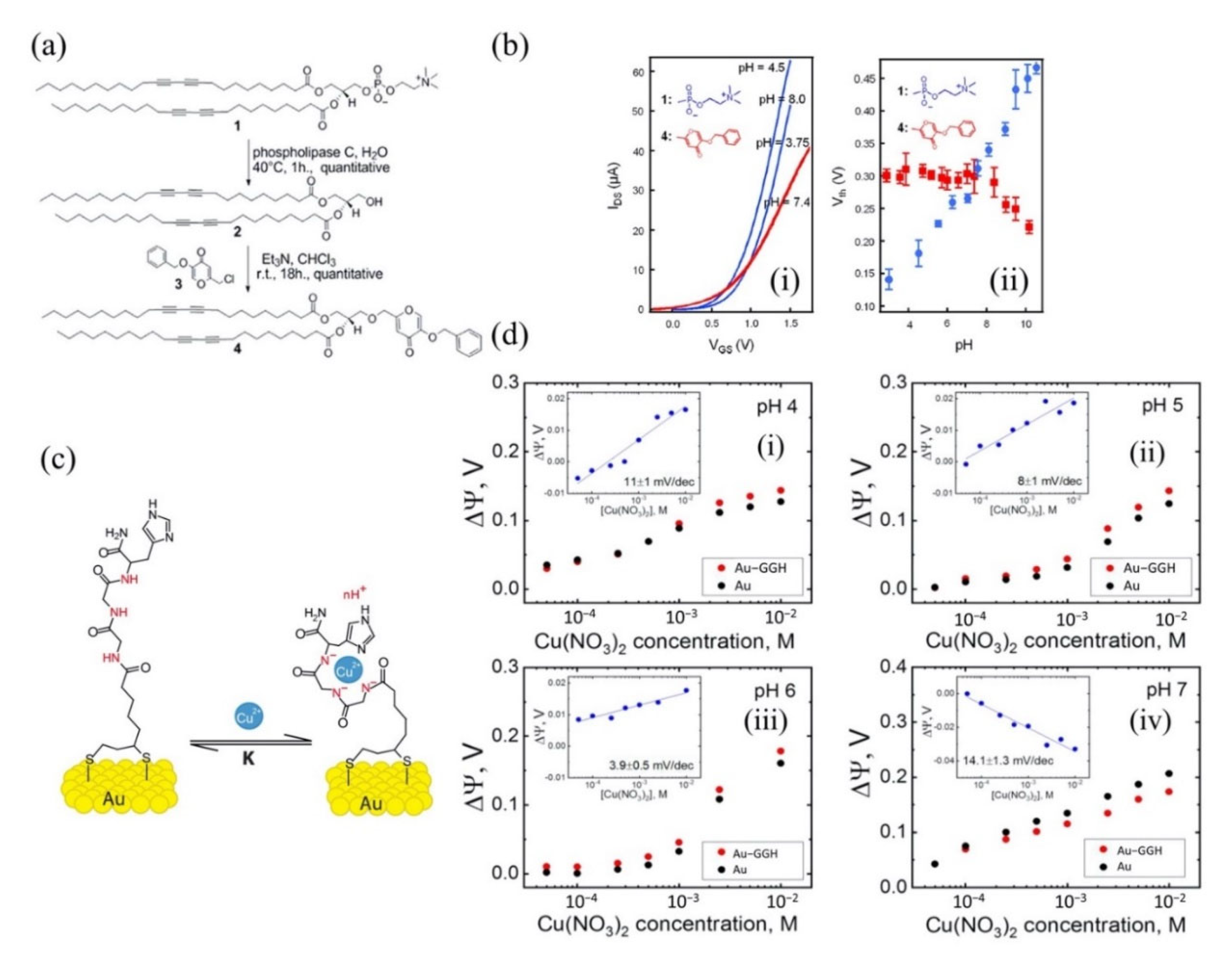
  104. Synhaivska, O.; Mermoud, Y.; Baghernejad, M.; Alshanski, I.; Hurevich, M.; Yitzchaik, S.; Wipf, M.; Calame, M. Detection of Cu2+ Ions with GGH Peptide Realized with Si-Nanoribbon ISFET. Sensors 2019, 19, 4022. [Google Scholar] [CrossRef] [Green Version]
  105. Le Borgne, B.; Girard, A.; Cardinaud, C.; Salaün, A.C.; Pichon, L.; Geneste, F. Covalent functionalization of polycrystalline silicon nanoribbons applied to Pb(II) electrical detection. Sens. Actuators B Chem. 2018, 268, 368–375. [Google Scholar] [CrossRef]
  106. Nair, P.R.; Alam, M.A. Screening-limited response of NanoBiosensors. Nano Lett. 2008, 8, 1281–1285. [Google Scholar] [CrossRef] [Green Version]
  107. Puglisi, D.; Eriksson, J.; Bur, C.; Schütze, A.; Spetz, A.L.; Andersson, M. Silicon carbide field effect transistors for detection of ultra-low concentrations of hazardous volatile organic compounds. Mater. Sci. Forum 2014, 778–780, 1067–1070. [Google Scholar] [CrossRef]
  108. Singh, A.; Amin, S.I.; Anand, S. Label Free Detection of Biomolecules Using SiGe Sourced Dual Electrode Doping-Less Dielectrically Modulated Tunnel FET. Silicon 2020, 12, 2301–2308. [Google Scholar] [CrossRef]
  109. Uno, T.; Tabata, H.; Kawal, T. Peptide-nucleic acid-modified ion-sensitive field-effect transistor-based biosensor for direct detection of DNA hybridization. Anal. Chem. 2007, 79, 52–59. [Google Scholar] [CrossRef]
  110. Iijima, S. Helical microtubules of graphitic carbon. Nature 1991, 354, 56–58. [Google Scholar] [CrossRef]
  111. Minot, E.D.; Janssens, A.M.; Heller, I.; Heering, H.A.; Dekker, C.; Lemay, S.G. Carbon nanotube biosensors: The critical role of the reference electrode. Appl. Phys. Lett. 2007, 91, 1–4. [Google Scholar] [CrossRef] [Green Version]
  112. Yao, X.; Zhang, Y.; Jin, W.; Hu, Y.; Cui, Y. Carbon nanotube field-effect transistor-based chemical and biological sensors. Sensors 2021, 21, 995. [Google Scholar] [CrossRef]
  113. Allen, B.L.; Kichambare, P.D.; Star, A. Carbon nanotube field-effect-transistor-based biosensors. Adv. Mater. 2007, 19, 1439–1451. [Google Scholar] [CrossRef]
  114. Oh, J.; Yoo, G.; Chang, Y.W.; Kim, H.J.; Jose, J.; Kim, E.; Pyun, J.C.; Yoo, K.H. A carbon nanotube metal semiconductor field effect transistor-based biosensor for detection of amyloid-beta in human serum. Biosens. Bioelectron. 2013, 50, 345–350. [Google Scholar] [CrossRef]
  115. Meyyappan, M. Carbon Nanotube-Based Chemical Sensors. Small 2016, 12, 2118–2129. [Google Scholar] [CrossRef] [PubMed]
  116. Kim, B.; Lee, J.; Namgung, S.; Kim, J.; Park, J.Y.; Lee, M.S.; Hong, S. DNA sensors based on CNT-FET with floating electrodes. Sens. Actuators B Chem. 2012, 169, 182–187. [Google Scholar] [CrossRef]
  117. Zhang, J. RNA-cleaving DNAzymes: Old catalysts with new tricks for intracellular and in vivo applications. Catalysts 2018, 8, 550. [Google Scholar] [CrossRef] [Green Version]
  118. Zhou, Y.; Tang, L.; Zeng, G.; Zhang, C.; Zhang, Y.; Xie, X. Current progress in biosensors for heavy metal ions based on DNAzymes/DNA molecules functionalized nanostructures: A review. Sens. Actuators B Chem. 2016, 223, 280–294. [Google Scholar] [CrossRef]
  119. Hu, L.; Fu, X.; Kong, G.; Yin, Y.; Meng, H.M.; Ke, G.; Zhang, X.B. DNAzyme-gold nanoparticle-based probes for biosensing and bioimaging. J. Mater. Chem. B 2020, 8, 9449–9465. [Google Scholar] [CrossRef]
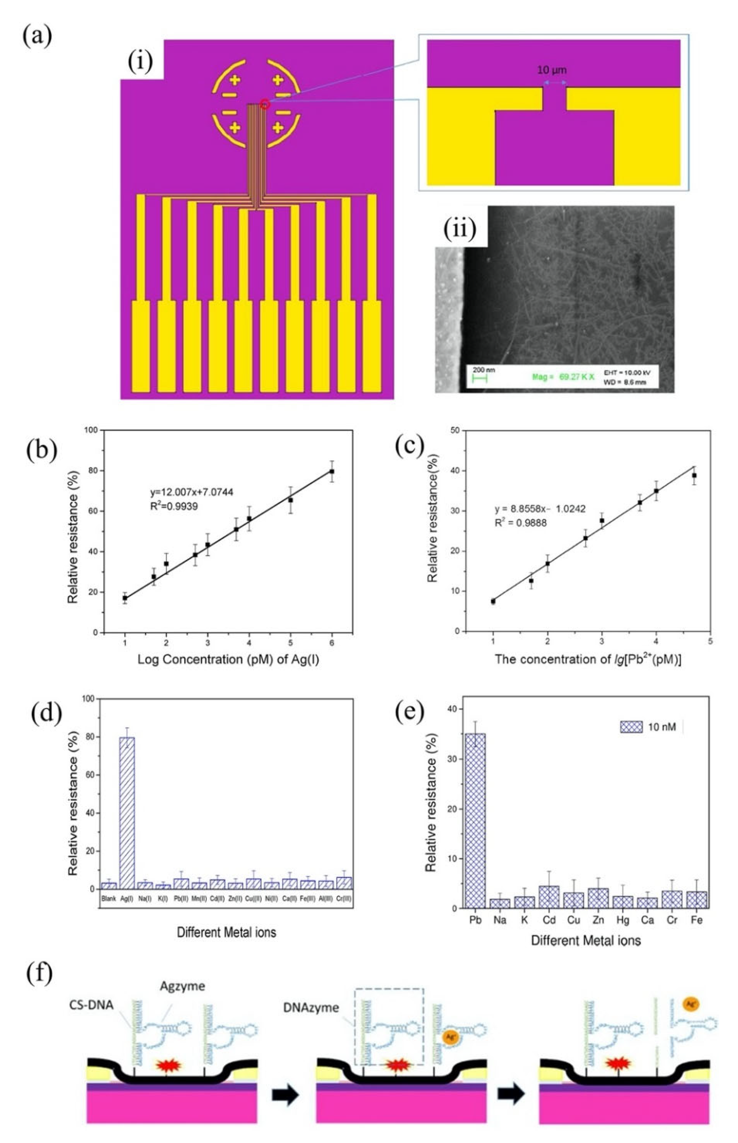
  120. Wang, H.; Liu, Y.; Liu, G. Label-free biosensor using a silver specific RNA-cleaving DNAzyme functionalized single-walled carbon nanotube for silver ion determination. Nanomaterials 2018, 8, 258. [Google Scholar] [CrossRef] [Green Version]
  121. Wang, H.; Yin, Y.; Gang, L. Single-gap Microelectrode Functionalized with Single-walled Carbon Nanotubes and Pbzyme for the Determination of Pb2+. Electroanalysis 2019, 31, 1174–1181. [Google Scholar] [CrossRef]
  122. Huang, X.; Li, J.; Zhang, Q.; Chen, S.; Xu, W.; Wu, J.; Niu, W.; Xue, J.; Li, C. A protease-free and signal-on electrochemical biosensor for ultrasensitive detection of lead ion based on GR-5 DNAzyme and catalytic hairpin assembly. J. Electroanal. Chem. 2018, 816, 75–82. [Google Scholar] [CrossRef]
  123. Lan, T.; Furuya, K.; Lu, Y. A highly selective lead sensor based on a classic lead DNAzyme. Chem. Commun. 2010, 46, 3896–3898. [Google Scholar] [CrossRef] [Green Version]
  124. Wang, H.; Liu, Y.; Wang, J.; Xiong, B.; Hou, X. Electrochemical impedance biosensor array based on DNAzyme-functionalized single-walled carbon nanotubes using Gaussian process regression for Cu(II) and Hg(II) determination. Microchim. Acta 2020, 187. [Google Scholar] [CrossRef]
  125. Yang, K.; Jin, H.; Chen, X.; Dai, J.; Wang, L.; Zhang, D. Soft sensor development for online quality prediction of industrial batch rubber mixing process using ensemble just-in-time Gaussian process regression models. Chemom. Intell. Lab. Syst. 2016, 155, 170–182. [Google Scholar] [CrossRef]
  126. Wang, H.; Zheng, S.; Nan, X.; Zhao, Y.; Wang, Y.; Zhang, F.; Yang, L.; Lixing, X.; Xiong, B. Non-specific DNAzyme-based biosensor with interfering ions for the Cd2+ determination in feed. Sens. Actuators B Chem. 2021, 329. [Google Scholar] [CrossRef]
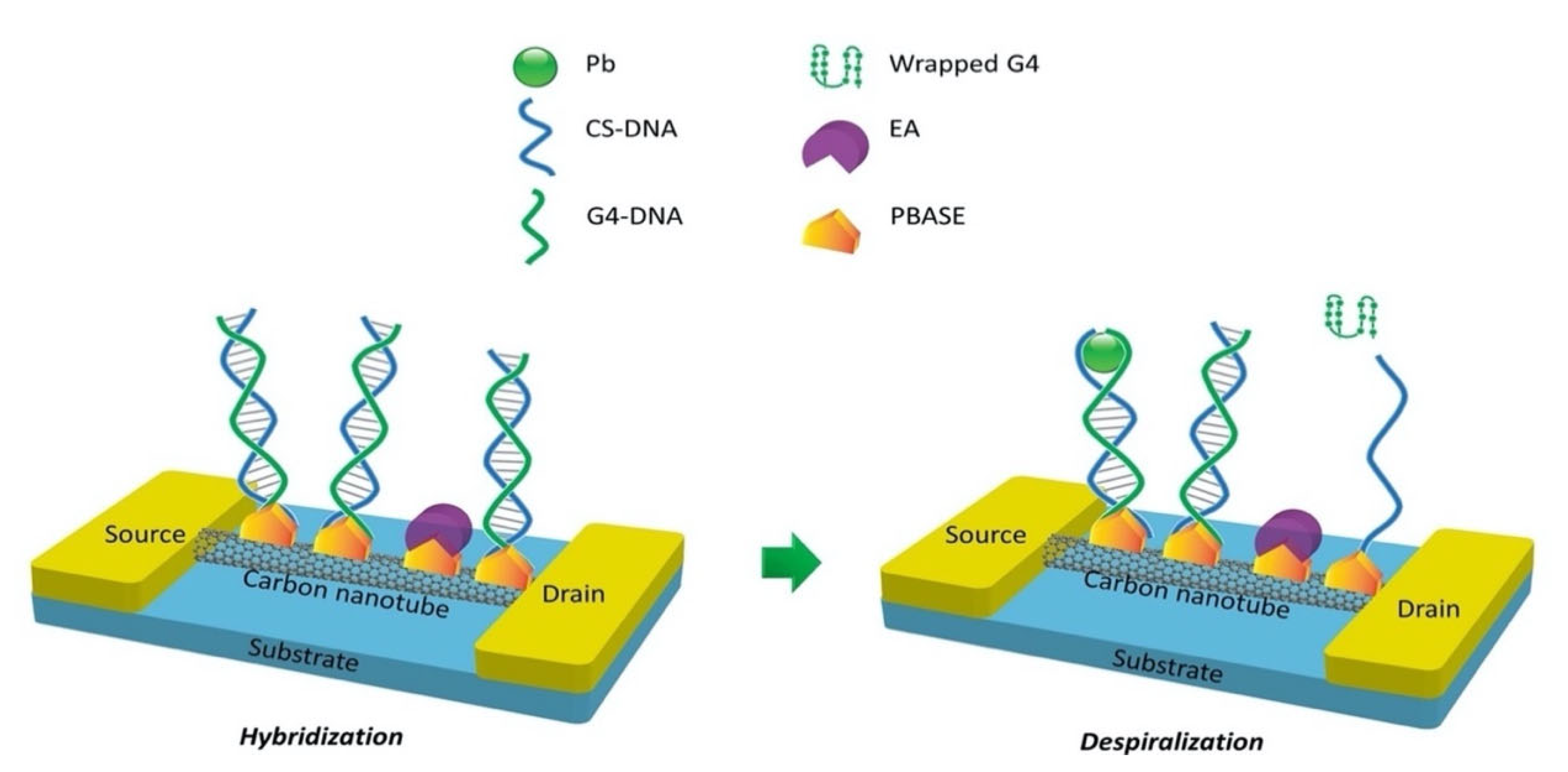
  127. Wang, H.; Liu, Y.; Liu, G. Reusable resistive aptasensor for Pb(II) based on the Pb(II)-induced despiralization of a DNA duplex and formation of a G-quadruplex. Microchim. Acta 2018, 185, 1–8. [Google Scholar] [CrossRef]
  128. Long, F.; Zhu, A.; Wang, H. Optofluidics-based DNA structure-competitive aptasensor for rapid on-site detection of lead(II) in an aquatic environment. Anal. Chim. Acta 2014, 849, 43–49. [Google Scholar] [CrossRef]
  129. Yang, D.; Liu, X.; Zhou, Y.; Luo, L.; Zhang, J.; Huang, A.; Mao, Q.; Chen, X.; Tang, L. Aptamer-based biosensors for detection of lead(ii) ion: A review. Anal. Methods 2017, 9, 1976–1990. [Google Scholar] [CrossRef]
  130. Reardan, D.T.; Meares, C.F.; Goodwin, D.A.; McTigue, M.; David, G.S.; Stone, M.R.; Leung, J.P.; Bartholomew, R.M.; Frincke, J.M. Antibodies against metal chelates. Nature 1985, 316, 265–268. [Google Scholar] [CrossRef]
  131. Wang, Y.; Zhang, C.; Liu, F. Antibody developments for metal ions and their applications. Food Agric. Immunol. 2020, 31, 1079–1103. [Google Scholar] [CrossRef]
  132. Cámara-Martos, F.; Da Costa, J.; Justino, C.I.L.; Cardoso, S.; Duarte, A.C.; Rocha-Santos, T. Disposable biosensor for detection of iron (III) in wines. Talanta 2016, 154, 80–84. [Google Scholar] [CrossRef]
  133. Ando, T. The electronic properties of graphene and carbon nanotubes. NPG Asia Mater. 2009, 1, 17–21. [Google Scholar] [CrossRef]
  134. Pinto, A.M.; Gonçalves, I.C.; Magalhães, F.D. Graphene-based materials biocompatibility: A review. Colloids Surfaces B Biointerfaces 2013, 111, 188–202. [Google Scholar] [CrossRef]
  135. Basu, J.; RoyChaudhuri, C. Graphene nanogrids FET immunosensor: Signal to noise ratio enhancement. Sensors 2016, 16, 1481. [Google Scholar] [CrossRef] [Green Version]
  136. Falina, S.; Syamsul, M.; Iyama, Y.; Hasegawa, M.; Koga, Y.; Kawarada, H. Carboxyl-functionalized graphene SGFET: pH sensing mechanism and reliability of anodization. Diam. Relat. Mater. 2019, 91, 15–21. [Google Scholar] [CrossRef]
  137. Zhang, T.; Cheng, Z.; Wang, Y.; Li, Z.; Wang, C.; Li, Y.; Fang, Y. Self-assembled 1-octadecanethiol monolayers on graphene for mercury detection. Nano Lett. 2010, 10, 4738–4741. [Google Scholar] [CrossRef]
  138. Patrick A., G.; Andrew R., K.; Xavier, M.; Victor J., M. Scanning tunnelling microscopy. J. Chem. Soc. Faraday Transcations 1994, 90, 2551–2554. [Google Scholar] [CrossRef]
  139. Sheng, H.Y.; Fujita, D.; Ohgi, T.; Dong, Z.C.; Jiang, Q.D.; Nejoh, H. Two-dimensional ordering of octadecanethiol molecules on graphite observed by scanning tunneling microscope. Appl. Surf. Sci. 1997, 121–122, 129–132. [Google Scholar] [CrossRef]
  140. Xu, Q.M.; Wan, L.J.; Yin, S.X.; Wang, C.; Bai, C.L. Effect of chemically modified tips on STM imaging of 1-octadecanethiol molecule. J. Phys. Chem. B 2001, 105, 10465–10467. [Google Scholar] [CrossRef]
  141. Afsharimani, N.; Uluutku, B.; Saygin, V.; Baykara, M.Z. Self-Assembled Molecular Films of Alkanethiols on Graphene for Heavy Metal Sensing. J. Phys. Chem. C 2018, 122, 474–480. [Google Scholar] [CrossRef] [Green Version]
  142. Kagi, J.H.; Kojima, Y. Metallothionein II―1987 Birkhauser Verlag Basel CHEMISTRY AND BIOCHEMISTRY OF METALLOTHIONEIN. Exp. Suppl. 1987, 52, 25–61. [Google Scholar]
  143. Chee, L.H.; Kumar, P.; Kang, C.H.; Burhanudin, Z.A. DNA/AuNP-graphene back-gated field effect transistor as a biosensor for lead (II) ion detection. Proc. 2017 IEEE Reg. Symp. Micro Nanoelectron. RSM 2017 2017, 127–130. [Google Scholar] [CrossRef]
  144. Priyadarshini, E.; Pradhan, N. Gold nanoparticles as efficient sensors in colorimetric detection of toxic metal ions: A review. Sens. Actuators B Chem. 2017, 238, 888–902. [Google Scholar] [CrossRef]
  145. Liu, W.; Zheng, B.; Cheng, S.; Fu, Y.; Li, W.; Lau, T.C.; Liang, H. G-quadruplex formation and sequence effect on the assembly of G-rich oligonucleotides induced by Pb2+ ions. Soft Matter 2012, 8, 7017–7023. [Google Scholar] [CrossRef]
  146. Li, Y.; Wang, C.; Zhu, Y.; Zhou, X.; Xiang, Y.; He, M.; Zeng, S. Fully integrated graphene electronic biosensor for label-free detection of lead (II) ion based on G-quadruplex structure-switching. Biosens. Bioelectron. 2017, 89, 758–763. [Google Scholar] [CrossRef] [PubMed]
  147. Stotzky, G. Persistence and Biological Activity in Soil of Insecticidal Proteins from Bacillus thuringiensis and of Bacterial DNA Bound on Clays and Humic Acids. J. Environ. Qual. 2000, 29, 691–705. [Google Scholar] [CrossRef]
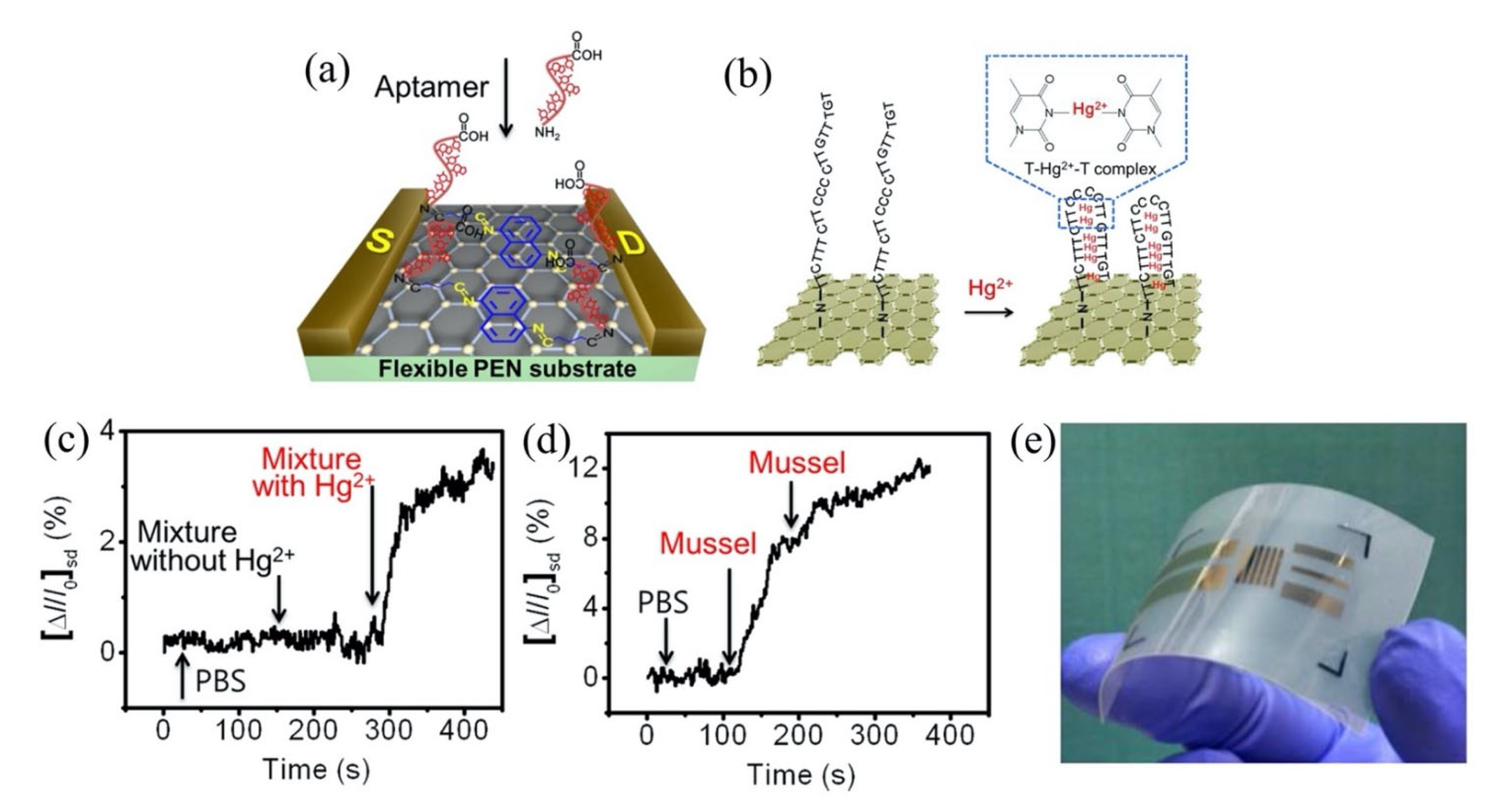
  148. Tu, J.; Gan, Y.; Liang, T.; Hu, Q.; Wang, Q.; Ren, T.; Sun, Q.; Wan, H.; Wang, P. Graphene FET array biosensor based on ssDNA aptamer for ultrasensitive Hg2+ detection in environmental pollutants. Front. Chem. 2018, 6. [Google Scholar] [CrossRef] [Green Version]
  149. An, J.H.; Park, S.J.; Kwon, O.S.; Bae, J.; Jang, J. High-performance flexible graphene aptasensor for mercury detection in mussels. ACS Nano 2013, 7, 10563–10571. [Google Scholar] [CrossRef]
  150. Besada, V.; Fumega, J.; Vaamonde, A. Temporal trends of Cd, Cu, Hg, Pb and Zn in mussel (Mytilus galloprovincialis) from the Spanish North-Atlantic coast 1991–1999. Sci. Total Environ. 2002, 288, 239–253. [Google Scholar] [CrossRef]
  151. Li, F.; Wang, Z.; Jia, Y. Reduced Carboxylate Graphene Oxide Based Field Effect Transistor as Pb2+ Aptamer Sensor. Micromachines 2019, 10, 388. [Google Scholar] [CrossRef] [Green Version]
  152. Wu, M.; Kempaiah, R.; Huang, P.J.; Maheshwari, V.; Liu, J. Adsorption and Desorption of DNA on Graphene Oxide Studied by Fluorescently Labeled Oligonucleotides. Langmuir 2011, 27, 2731–2738. [Google Scholar] [CrossRef] [Green Version]
  153. Park, J.S.; Goo, N.I.; Kim, D.E. Mechanism of DNA Adsorption and Desorption on Graphene Oxide. Langmuir 2014, 30, 12587–12595. [Google Scholar] [CrossRef]
  154. Wen, Y.; Li, F.Y.; Dong, X.; Zhang, J.; Xiong, Q.; Chen, P. The Electrical Detection of Lead Ions Using Gold-Nanoparticle- and DNAzyme-Functionalized Graphene Device. Adv. Healthc. Mater. 2012, 2, 271–274. [Google Scholar] [CrossRef]
  155. Liang, G.; Man, Y.; Li, A.; Jin, X.; Liu, X.; Pan, L. DNAzyme-based biosensor for detection of lead ion: A review. Microchem. J. 2017, 131, 145–153. [Google Scholar] [CrossRef]
  156. Zhang, X.B.; Kong, R.M.; Lu, Y. Metal ion sensors based on DNAzymes and related DNA molecules. Annu. Rev. Anal. Chem. 2011, 4, 105–128. [Google Scholar] [CrossRef] [Green Version]
  157. Wang, C.; Cui, X.; Li, Y.; Li, H.; Huang, L.; Bi, J.; Luo, J.; Ma, L.Q.; Zhou, W.; Cao, Y.; et al. A label-free and portable graphene FET aptasensor for children blood lead detection. Sci. Rep. 2016, 6, 1–8. [Google Scholar] [CrossRef]
  158. Chang, J.; Zhou, G.; Gao, X.; Mao, S.; Cui, S.; Ocola, L.E.; Yuan, C.; Chen, J. Real-time detection of mercury ions in water using a reduced graphene oxide/DNA field-effect transistor with assistance of a passivation layer. Sens. Bio-Sens. Res. 2015, 5, 97–104. [Google Scholar] [CrossRef]
  159. Tanaka, Y.; Oda, S.; Yamaguchi, H.; Kondo, Y.; Kojima, C.; Ono, A. 15 N-15 N J-coupling across HgII: Direct observation of HgII-mediated T-T base pairs in a DNA duplex. J. Am. Chem. Soc. 2007, 129, 244–245. [Google Scholar] [CrossRef]
  160. Clever, G.H.; Kaul, C.; Carell, T. DNA-metal base pairs. Angew. Chemie Int. Ed. 2007, 46, 6226–6236. [Google Scholar] [CrossRef]
  161. Zhu, Z.; Su, Y.; Li, J.; Li, D.; Zhang, J.; Song, S.; Zhao, Y.; Li, G.; Fan, C. Highly sensitive electrochemical sensor for mercury(II) ions by using a mercury-specific oligonucleotide probe and gold nanoparticle-based amplification. Anal. Chem. 2009, 81, 7660–7666. [Google Scholar] [CrossRef]
  162. Zhou, G.; Chang, J.; Cui, S.; Pu, H.; Wen, Z.; Chen, J. Real-time, selective detection of Pb2+ in water using a reduced graphene oxide/gold nanoparticle field-effect transistor device. ACS Appl. Mater. Interfaces 2014, 6, 19235–19241. [Google Scholar] [CrossRef]
  163. Sui, X.; Pu, H.; Maity, A.; Chang, J.; Jin, B.; Lu, G.; Wang, Y.; Ren, R.; Mao, S.; Chen, J. Field-Effect Transistor Based on Percolation Network of Reduced Graphene Oxide for Real-Time ppb-Level Detection of Lead Ions in Water. ECS J. Solid State Sci. Technol. 2020, 9, 115012. [Google Scholar] [CrossRef]
  164. Maity, A.; Sui, X.; Tarman, C.R.; Pu, H.; Chang, J.; Zhou, G.; Ren, R.; Mao, S.; Chen, J. Pulse-Driven Capacitive Lead Ion Detection with Reduced Graphene Oxide Field-Effect Transistor Integrated with an Analyzing Device for Rapid Water Quality Monitoring. ACS Sens. 2017, 2, 1653–1661. [Google Scholar] [CrossRef]
  165. Chen, K.; Lu, G.; Chang, J.; Mao, S.; Yu, K.; Cui, S.; Chen, J. Hg(II) Ion Detection using Thermally Reduced Graphene Oxide Decorated with Functionalized Gold Nanoparticles. Anal. Chem. 2012, 84, 4057–4062. [Google Scholar] [CrossRef]
  166. Takagiri, Y.; Ikuta, T.; Maehashi, K. Selective Detection of Cu2+ Ions by Immobilizing Thiacalix[4]arene on Graphene Field-Effect Transistors. ACS Omega 2019, 5, 877–881. [Google Scholar] [CrossRef] [Green Version]
  167. Sudibya, H.G.; He, Q.; Zhang, H.; Chen, P. Electrical detection of metal ions using field-effect transistors based on micropatterned reduced graphene oxide films. ACS Nano 2011, 5, 1990–1994. [Google Scholar] [CrossRef]
  168. Li, P.; Liu, B.; Zhang, D.; Sun, Y.; Liu, J. Graphene field-effect transistors with tunable sensitivity for high performance Hg (II) sensing. Appl. Phys. Lett. 2016, 109, 1–6. [Google Scholar] [CrossRef]
  169. Ayesh, A.I.; Karam, Z.; Awwad, F.; Meetani, M.A. Conductometric graphene sensors decorated with nanoclusters for selective detection of Hg2+ traces in water. Sens. Actuators B Chem. 2015, 221, 201–206. [Google Scholar] [CrossRef]
  170. Eickhoff, M.; Schalwig, J.; Steinhoff, G.; Weidemann, O.; Görgens, L.; Neuberger, R.; Hermann, M.; Baur, B.; Müller, G.; Ambacher, O.; et al. Electronics and sensors based on pyroelectric AlGaN/GaN heterostructures: Part B: Sensor applications. Phys. Status Solidi C Conf. 2003, 0, 1908–1918. [Google Scholar] [CrossRef]
  171. Bosacchi, A.; Franchi, S.; Gombia, E.; Mosca, R.; Fantini, F.; Franchi, S.; Menozzi, R. Thermal Stability of Al/GaAs and AI/GaAs/AIGaAs(MBE) Schottky Barriers. Electron. Lett. 1993, 29, 651–653. [Google Scholar] [CrossRef]
  172. Dammann, M.; Leuther, A.; Benkhelifa, F.; Feltgen, T.; Jantz, W. Reliability and degradation mechanism of AlGaAs/InGaAs and InAlAs/InGaAs HEMTs. Phys. Status Solidi Appl. Res. 2003, 195, 81–86. [Google Scholar] [CrossRef]
  173. Kikkawa, T.; Makiyama, K.; Ohki, T.; Kanamura, M.; Imanishi, K.; Hara, N.; Joshin, K. High performance and high reliability AlGaN/GaN HEMTs. Phys. Status Solidi Appl. Mater. Sci. 2009, 206, 1135–1144. [Google Scholar] [CrossRef]
  174. Shiojima, K.; Shigekawa, N. Thermal Stability of Electrical Properties in AlGaN/GaN Heterostructures. Jpn. J. Appl. Phys. Part 1 Regul. Pap. Short Notes Rev. Pap. 2004, 43, 100–105. [Google Scholar] [CrossRef]
  175. Vuong, T.A.; Cha, H.Y.; Kim, H. Response enhancement of pt–algan/gan hemt gas sensors by thin algan barrier with the source-connected gate configuration at high temperature. Micromachines 2021, 12, 537. [Google Scholar] [CrossRef] [PubMed]
  176. Sarangadharan, I.; Regmi, A.; Chen, Y.W.; Hsu, C.P.; Chen, P.C.; Chang, W.H.; Lee, G.Y.; Chyi, J.I.; Shiesh, S.C.; Lee, G.B.; et al. High sensitivity cardiac troponin I detection in physiological environment using AlGaN/GaN High Electron Mobility Transistor (HEMT) Biosensors. Biosens. Bioelectron. 2018, 100, 282–289. [Google Scholar] [CrossRef] [PubMed]
  177. Jia, X.; Chen, D.; Bin, L.; Lu, H.; Zhang, R.; Zheng, Y. Highly selective and sensitive phosphate anion sensors based on AlGaN/GaN high electron mobility transistors functionalized by ion imprinted polymer. Sci. Rep. 2016, 6, 1–7. [Google Scholar] [CrossRef] [PubMed]
  178. Bolotin, K.I.; Sikes, K.J.; Jiang, Z.; Klima, M.; Fudenberg, G.; Hone, J.; Kim, P.; Stormer, H.L. Ultrahigh electron mobility in suspended graphene. Solid State Commun. 2008, 146, 351–355. [Google Scholar] [CrossRef] [Green Version]
  179. Siddique, A.; Ahmed, R.; Anderson, J.; Holtz, M.; Piner, E.L. Improved Electrical Properties of AlGaN/GaN High-Electron-Mobility Transistors by in Situ Tailoring the SiNxPassivation Layer. ACS Appl. Mater. Interfaces 2021, 13, 18264–18273. [Google Scholar] [CrossRef]
  180. Tai, T.Y.; Sinha, A.; Sarangadharan, I.; Pulikkathodi, A.K.; Wang, S.L.; Lee, G.Y.; Chyi, J.I.; Shiesh, S.C.; Lee, G.B.; Wang, Y.L. Design and Demonstration of Tunable Amplified Sensitivity of AlGaN/GaN High Electron Mobility Transistor (HEMT)-Based Biosensors in Human Serum. Anal. Chem. 2019, 91, 5953–5960. [Google Scholar] [CrossRef]
  181. Sokolovskij, R.; Zhang, J.; Zheng, H.; Li, W.; Jiang, Y.; Yang, G.; Yu, H.; Sarro, P.M.; Zhang, G. The Impact of Gate Recess on the H Detection Properties of Pt-AlGaN/GaN HEMT Sensors. IEEE Sens. J. 2020, 20, 8947–8955. [Google Scholar] [CrossRef]
  182. Wang, C.; Zhang, Y.; Guan, M.; Cui, L.; Ding, K.; Zhang, B.; Lin, Z.; Huang, F.; Zeng, Y. Specific detection of mercury(II) irons using AlGaAs/InGaAs high electron mobility transistors. J. Cryst. Growth 2015, 425, 381–384. [Google Scholar] [CrossRef]
  183. Nigam, A.; Bhat, T.N.; Bhati, V.S.; Dolmanan, S.B.; Tripathy, S.; Kumar, M. MPA-GSH Functionalized AlGaN/GaN High-Electron Mobility Transistor-Based Sensor for Cadmium Ion Detection. IEEE Sens. J. 2019, 19, 2863–2870. [Google Scholar] [CrossRef]
  184. Leverrier, P.; Montigny, C.; Garrigos, M.; Champeil, P. Metal binding to ligands: Cadmium complexes with glutathione revisited. Anal. Biochem. 2007, 371, 215–228. [Google Scholar] [CrossRef]
  185. Díaz-Cruz, M.S.; Mendieta, J.; Tauler, R.; Esteban, M. Cadmium-binding properties of glutathione: A chemometrical analysis of voltammetric data. J. Inorg. Biochem. 1997, 66, 29–36. [Google Scholar] [CrossRef]
  186. Pei, K.L.; Sooriyaarachchi, M.; Sherrell, D.A.; George, G.N.; Gailer, J. Probing the coordination behavior of Hg2+, CH3Hg+, and Cd2+ towards mixtures of two biological thiols by HPLC-ICP-AES. J. Inorg. Biochem. 2011, 105, 375–381. [Google Scholar] [CrossRef]
  187. Guo, Y.; Zhang, Y.; Shao, H.; Wang, Z.; Wang, X.; Jiang, X. Label-free colorimetric detection of cadmium ions in rice samples using gold nanoparticles. Anal. Chem. 2014, 86, 8530–8534. [Google Scholar] [CrossRef]
  188. Chow, E.; Hibbert, D.B.; Gooding, J.J. Voltammetric detection of cadmium ions at glutathione-modified gold electrodes. Analyst 2005, 130, 831–837. [Google Scholar] [CrossRef]
  189. Nigam, A.; Bhati, V.S.; Bhat, T.N.; Dolmanan, S.B.; Tripathy, S.; Kumar, M. Sensitive and Selective Detection of Pb2+ Ions Using 2,5-Dimercapto-1,3,4-Thiadiazole Functionalized AlGaN/GaN High Electron Mobility Transistor. IEEE Electron Device Lett. 2019, 40, 1976–1979. [Google Scholar] [CrossRef]
  190. Wu, Y.; Bing Li, N.; Qun Luo, H. Electrochemical determination of Pb(II) at a gold electrode modified with a self-assembled monolayer of 2,5-dimercapto-1,3,4-thiadiazole. Microchim. Acta 2008, 160, 185–190. [Google Scholar] [CrossRef]
  191. He, X.; Su, Z.; Xie, Q.; Chen, C.; Fu, Y.; Chen, L.; Liu, Y.; Ma, M.; Deng, L.; Qin, D.; et al. Differential pulse anodic stripping voltammetric determination of Cd and Pb at a bismuth glassy carbon electrode modified with Nafion, poly(2,5-dimercapto-1,3,4-thiadiazole) and multiwalled carbon nanotubes. Microchim. Acta 2011, 173, 95–102. [Google Scholar] [CrossRef]
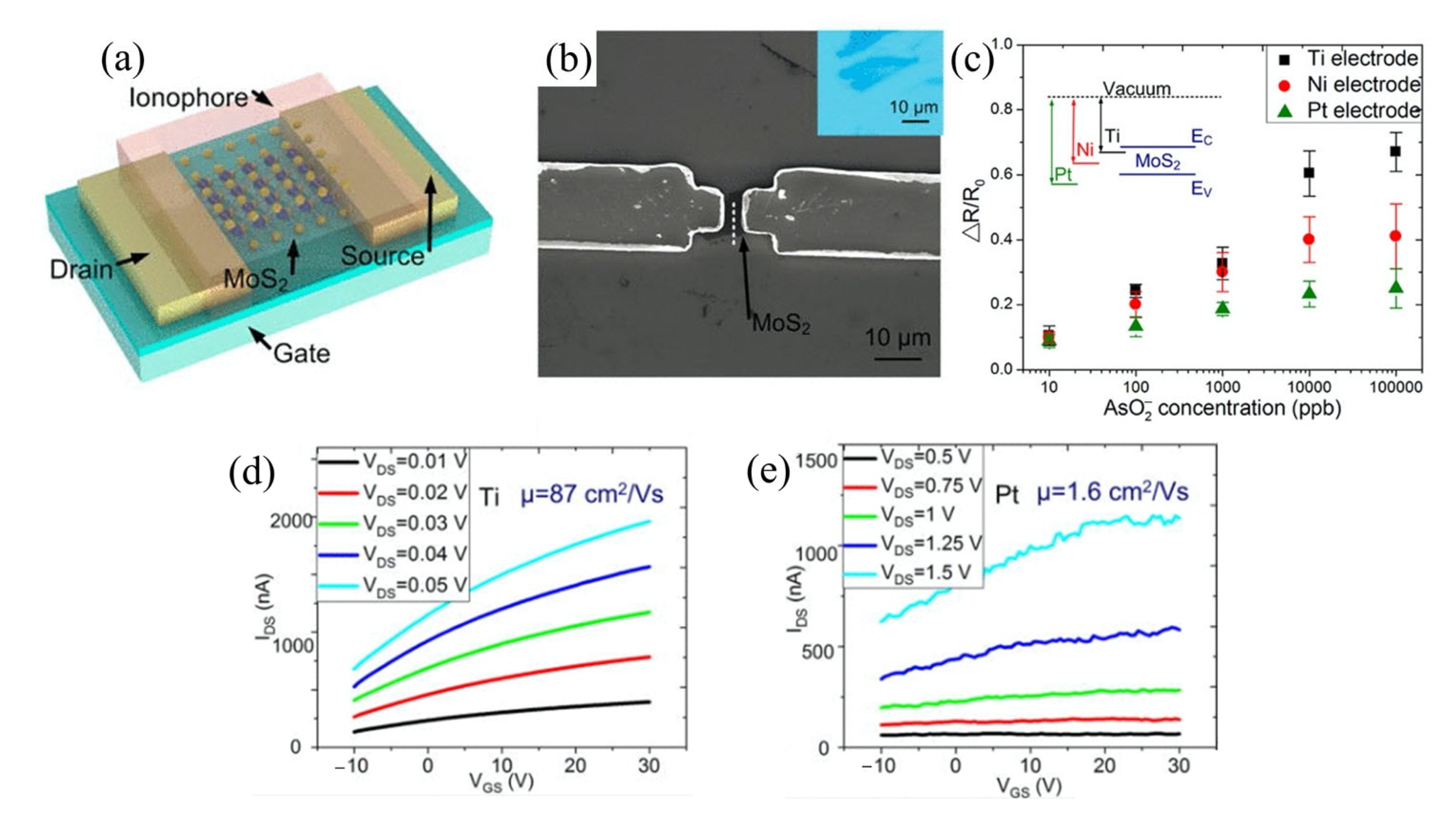
  192. Nigam, A.; Goel, N.; Bhat, T.N.; Tawabur Rahman, M.; Dolmanan, S.B.; Qiao, Q.; Tripathy, S.; Kumar, M. Real time detection of Hg2+ ions using MoS2 functionalized AlGaN/GaN high electron mobility transistor for water quality monitoring. Sensors Actuators, B Chem. 2020, 309, 127832. [Google Scholar] [CrossRef]
  193. Bakker, E.; Bühlmann, P.; Pretsch, E. Carrier-based ion-selective electrodes and bulk optodes. 1. General characteristics. Chem. Rev. 1997, 97, 3083–3132. [Google Scholar] [CrossRef]
  194. Bühlmann, P.; Pretsch, E.; Bakker, E. Carrier-based ion-selective electrodes and bulk optodes. 2. Ionophores for potentiometric and optical sensors. Chem. Rev. 1998, 98, 1593–1687. [Google Scholar] [CrossRef]
  195. Maehashi, K.; Sofue, Y.; Okamoto, S.; Ohno, Y.; Inoue, K.; Matsumoto, K. Selective ion sensors based on ionophore-modified graphene field-effect transistors. Sens. Actuators B Chem. 2013, 187, 45–49. [Google Scholar] [CrossRef]
  196. Zuliani, C.; Diamond, D. Opportunities and challenges of using ion-selective electrodes in environmental monitoring and wearable sensors. Electrochim. Acta 2012, 84, 29–34. [Google Scholar] [CrossRef] [Green Version]
  197. Kamenica, M.; Kothur, R.R.; Willows, A.; Patel, B.A.; Cragg, P.J. Lithium ion sensors. Sensors 2017, 17, 2430. [Google Scholar] [CrossRef] [Green Version]
  198. Singh, A.K.; Jain, A.K.; Upadhyay, A.; Thomas, K.R.J.; Singh, P. Electroanalytical performance of Cd(II) selective sensor based on PVC membranes of 5,5′-(5,5′-benzo[c][1,2,5]thiadiazole-4,7-diyl)bis(thiophene-5,2-diyl))bis(N1,N1,N3,N3-tetraphenylbenzene-1,3-diamine). Int. J. Environ. Anal. Chem. 2013, 93, 813–827. [Google Scholar] [CrossRef]
  199. Kondratyeva, Y.O.; Tolstopjatova, E.G.; Kirsanov, D.O.; Mikhelson, K.N. Chronoamperometric and coulometric analysis with ionophore-based ion-selective electrodes: A modified theory and the potassium ion assay in serum samples. Sens. Actuators B Chem. 2020, 310, 127894. [Google Scholar] [CrossRef]
  200. Chen, Y.-T.; Hseih, C.-Y.; Sarangadharan, I.; Sukesan, R.; Lee, G.-Y.; Chyi, J.-I.; Wang, Y.-L. Beyond the Limit of Ideal Nernst Sensitivity: Ultra-High Sensitivity of Heavy Metal Ion Detection with Ion-Selective High Electron Mobility Transistors. ECS J. Solid State Sci. Technol. 2018, 7, Q176–Q183. [Google Scholar] [CrossRef]
  201. Chen, Y.-T.; Sarangadharan, I.; Sukesan, R.; Hseih, C.Y.; Lee, G.Y.; Chyi, J.I.; Wang, Y.L. High-field modulated ion-selective field-effect-Transistor (FET) sensors with sensitivity higher than the ideal Nernst sensitivity. Sci. Rep. 2018, 8, 1–11. [Google Scholar] [CrossRef] [Green Version]
  202. Hsieh, C.-Y.; Chen, Y.-T.; Sukesan, R.; Wang, Y.-L. Ultra-High Sensitivity for Lead Ion Detection Beyond the Ideal Nernst Response with AlGaN/GaN High Electron Mobility Transistors (HEMTs). ECS Trans. 2018, 85, 3–8. [Google Scholar] [CrossRef]
  203. Sukesan, R.; Chen, Y.-T.; Wang, Y.-L. Mercury Selective GaN HEMT Sensor for Dynamic Water Quality Monitoring. ECS Trans. 2017, 80, 953–957. [Google Scholar] [CrossRef]
  204. Sarangadharan, I.; Pulikkathodi, A.K.; Chu, C.-H.; Chen, Y.-W.; Regmi, A.; Chen, P.-C.; Hsu, C.-P.; Wang, Y.-L. Review—High Field Modulated FET Biosensors for Biomedical Applications. ECS J. Solid State Sci. Technol. 2018, 7, Q3032–Q3042. [Google Scholar] [CrossRef]
  205. Chu, C.H.; Sarangadharan, I.; Regmi, A.; Chen, Y.W.; Hsu, C.P.; Chang, W.H.; Lee, G.Y.; Chyi, J.I.; Chen, C.C.; Shiesh, S.C.; et al. Beyond the Debye length in high ionic strength solution: Direct protein detection with field-effect transistors (FETs) in human serum. Sci. Rep. 2017, 7, 1–15. [Google Scholar] [CrossRef] [PubMed]
  206. Sukesan, R.; Chen, Y.T.; Shahim, S.; Wang, S.L.; Sarangadharan, I.; Wang, Y.L. Instant mercury ion detection in industrial waste water with a microchip using extended gate field-effect transistors and a portable device. Sensors 2019, 19, 2209. [Google Scholar] [CrossRef] [PubMed] [Green Version]
  207. Ambacher, O.; Smart, J.; Shealy, J.R.; Weimann, N.G.; Chu, K.; Murphy, M.; Schaff, W.J.; Eastman, L.F.; Dimitrov, R.; Wittmer, L.; et al. Two-dimensional electron gases induced by spontaneous and piezoelectric polarization charges in N- And Ga-face AIGaN/GaN heterostructures. J. Appl. Phys. 1999, 85, 3222–3233. [Google Scholar] [CrossRef] [Green Version]
  208. Asadnia, M.; Myers, M.; Akhavan, N.D.; O’Donnell, K.; Umana-Membreno, G.A.; Mishra, U.K.; Nener, B.; Baker, M.; Parish, G. Mercury(II) selective sensors based on AlGaN/GaN transistors. Anal. Chim. Acta 2016, 943, 1–7. [Google Scholar] [CrossRef] [Green Version]
  209. Gu, L.; Yang, S.; Miao, B.; Gu, Z.; Wang, J.; Sun, W.; Wu, D.; Li, J. Electrical detection of trace zinc ions with an extended gate-AlGaN/GaN high electron mobility sensor. Analyst 2019, 144, 663–668. [Google Scholar] [CrossRef]
  210. Cheng, J.; Li, J.; Miao, B.; Wang, J.; Wu, Z.; Wu, D.; Pei, R. Ultrasensitive detection of Hg2+ using oligonucleotide- functionalized AlGaN/GaN high electron mobility transistor. Appl. Phys. Lett. 2014, 105. [Google Scholar] [CrossRef]
  211. Ren, F.; Pearton, S.J. Sensors using AlGaN/GaN based high electron mobility transistor for environmental and bio-applications. Phys. Status Solidi Curr. Top. Solid State Phys. 2012, 9, 393–398. [Google Scholar] [CrossRef]
  212. Niu, J.; Zhang, Y.; Guan, M.; Wang, C.; Cui, L.; Yang, Q.; Li, Y.; Zeng, Y. Detection of lead ions with AlGaAs/InGaAs pseudomorphic high electron mobility transistor. J. Semicond. 2016, 37. [Google Scholar] [CrossRef]
  213. Pumera, M.; Loo, A.H. Layered transition-metal dichalcogenides (MoS2 and WS2) for sensing and biosensing. TrAC Trends Anal. Chem. 2014, 61, 49–53. [Google Scholar] [CrossRef]
  214. Mao, S.; Chang, J.; Pu, H.; Lu, G.; He, Q.; Zhang, H.; Chen, J. Two-dimensional nanomaterial-based field-effect transistors for chemical and biological sensing. Chem. Soc. Rev. 2017, 46, 6872–6904. [Google Scholar] [CrossRef]
  215. Li, M.-Z.; Han, S.-T.; Zhou, Y. Recent Advances in Flexible Field-Effect Transistors toward Wearable Sensors. Adv. Intell. Syst. 2020, 2, 2000113. [Google Scholar] [CrossRef]
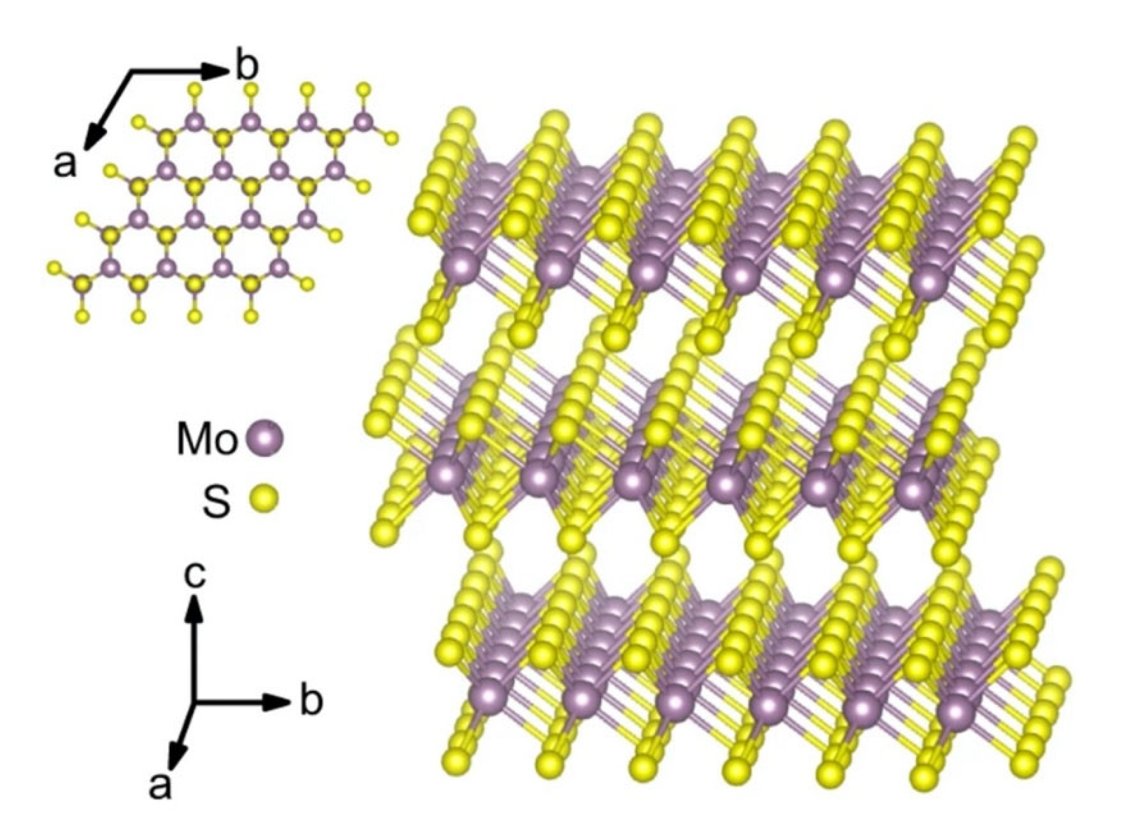
  216. Dickinson, R.G.; Pauling, L. The crystal structure of molybdenite. J. Am. Chem. Soc. 1923, 45, 1466–1471. [Google Scholar] [CrossRef]
  217. Ermolaev, G.A.; Grudinin, D.V.; Stebunov, Y.V.; Voronin, K.V.; Kravets, V.G.; Duan, J.; Mazitov, A.B.; Tselikov, G.I.; Bylinkin, A.; Yakubovsky, D.I.; et al. Giant optical anisotropy in transition metal dichalcogenides for next-generation photonics. Nat. Commun. 2021, 12, 1–8. [Google Scholar] [CrossRef]
  218. Manzeli, S.; Ovchinnikov, D.; Pasquier, D.; Yazyev, O.V.; Kis, A. 2D transition metal dichalcogenides. Nat. Rev. Mater. 2017, 2. [Google Scholar] [CrossRef]
  219. Radisavljevic, B.; Radenovic, A.; Brivio, J.; Giacometti, V.; Kis, A. Single-layer MoS2 transistors. Nat. Nanotechnol. 2011, 6, 147–150. [Google Scholar] [CrossRef]
  220. Zhou, G.; Chang, J.; Pu, H.; Shi, K.; Mao, S.; Sui, X.; Ren, R.; Cui, S.; Chen, J. Ultrasensitive Mercury Ion Detection Using DNA-Functionalized Molybdenum Disulfide Nanosheet/Gold Nanoparticle Hybrid Field-Effect Transistor Device. ACS Sens. 2016, 1, 295–302. [Google Scholar] [CrossRef]
  221. Gong, J.; Zhou, T.; Song, D.; Zhang, L. Monodispersed Au nanoparticles decorated graphene as an enhanced sensing platform for ultrasensitive stripping voltammetric detection of mercury(II). Sens. Actuators B Chem. 2010, 150, 491–497. [Google Scholar] [CrossRef]
  222. Mahajan, R.K.; Kaur, I.; Lobana, T.S. A mercury(II) ion-selective electrode based on neutral salicylaldehyde thiosemicarbazone. Talanta 2003, 59, 101–105. [Google Scholar] [CrossRef]
  223. Jiang, S.; Cheng, R.; Ng, R.; Huang, Y.; Duan, X. Highly sensitive detection of mercury(II) ions with few-layer molybdenum disulfide. Nano Res. 2015, 8, 257–262. [Google Scholar] [CrossRef]
  224. Li, P.; Zhang, D.; Sun, Y.; Chang, H.; Liu, J.; Yin, N. Towards intrinsic MoS2 devices for high performance arsenite sensing. Appl. Phys. Lett. 2016, 109. [Google Scholar] [CrossRef] [Green Version]
  225. Lee, J.; Dak, P.; Lee, Y.; Park, H.; Choi, W.; Alam, M.A.; Kim, S. Two-dimensional layered MoS2 biosensors enable highly sensitive detection of biomolecules. Sci. Rep. 2014, 4, 1–7. [Google Scholar] [CrossRef] [Green Version]
  226. Liu, B.; Chen, L.; Liu, G.; Abbas, A.N.; Fathi, M.; Zhou, C. High-performance chemical sensing using Schottky-contacted chemical vapor deposition grown monolayer MoS2 transistors. ACS Nano 2014, 8, 5304–5314. [Google Scholar] [CrossRef]
  227. Li, P.; Zhang, D.; Wu, Z. Flexible MoS2 sensor arrays for high performance label-free ion sensing. Sens. Actuators A Phys. 2019, 286, 51–58. [Google Scholar] [CrossRef]
  228. Tsai, M.Y.; Tarasov, A.; Hesabi, Z.R.; Taghinejad, H.; Campbell, P.M.; Joiner, C.A.; Adibi, A.; Vogel, E.M. Flexible MoS2 Field-Effect Transistors for Gate-Tunable Piezoresistive Strain Sensors. ACS Appl. Mater. Interfaces 2015, 7, 12850–12855. [Google Scholar] [CrossRef]
  229. Manzeli, S.; Allain, A.; Ghadimi, A.; Kis, A. Piezoresistivity and Strain-induced Band Gap Tuning in Atomically Thin MoS2. Nano Lett. 2015, 15, 5330–5335. [Google Scholar] [CrossRef] [Green Version]
  230. Wu, W.; Wang, L.; Li, Y.; Zhang, F.; Lin, L.; Niu, S.; Chenet, D.; Zhang, X.; Hao, Y.; Heinz, T.F.; et al. Piezoelectricity of single-atomic-layer MoS2 for energy conversion and piezotronics. Nature 2014, 514, 470–474. [Google Scholar] [CrossRef]
  231. John, A.P.; Thenapparambil, A.; Thalakulam, M. Strain-engineering the Schottky barrier and electrical transport on MoS2. Nanotechnology 2020, 31, 1–14. [Google Scholar] [CrossRef] [Green Version]
  232. Bazylewski, P.; Van Middelkoop, S.; Divigalpitiya, R.; Fanchini, G. Solid-State Chemiresistors from Two-Dimensional MoS2 Nanosheets Functionalized with l-Cysteine for In-Line Sensing of Part-Per-Billion Cd2+ Ions in Drinking Water. ACS Omega 2020, 5, 643–649. [Google Scholar] [CrossRef] [Green Version]
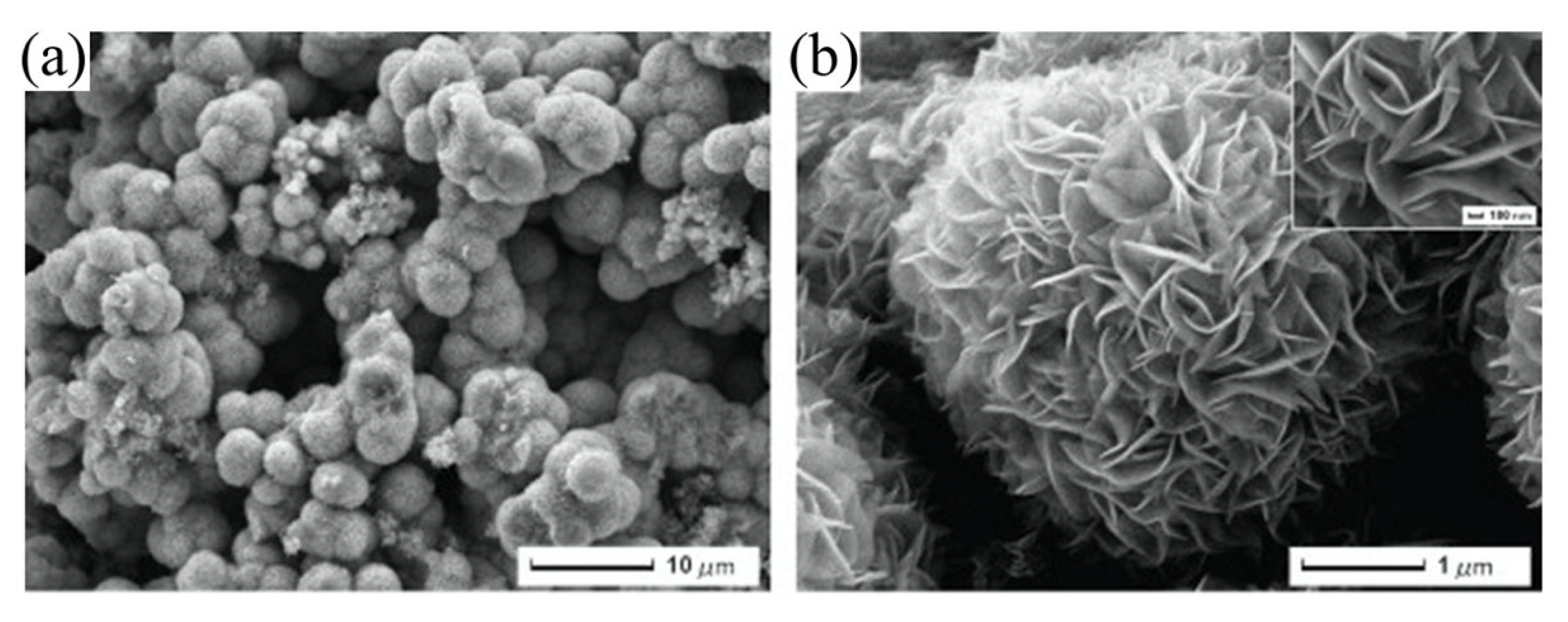
  233. An, J.H.; Jang, J. A highly sensitive FET-type aptasensor using flower-like MoS2 nanospheres for real-time detection of arsenic(III). Nanoscale 2017, 9, 7483–7492. [Google Scholar] [CrossRef]
  234. Zhang, X.; Huang, X.; Xue, M.; Ye, X.; Lei, W.; Tang, H.; Li, C. Hydrothermal synthesis and characterization of 3D flower-like MoS2 microspheres. Mater. Lett. 2015, 148, 67–70. [Google Scholar] [CrossRef]
  235. Neog, A.; Deb, S.; Biswas, R. Atypical electrical behavior of few layered WS2 nanosheets based platform subject to heavy metal ion treatment. Mater. Lett. 2020, 268. [Google Scholar] [CrossRef] [Green Version]
  236. Neog, A.; Biswas, R. WS2 nanosheets as a potential candidate towards sensing heavy metal ions: A new dimension of 2D materials. Mater. Res. Bull. 2021, 144, 111471. [Google Scholar] [CrossRef]
  237. Anju, S.; Ashtami, J.; Mohanan, P.V. Black phosphorus, a prospective graphene substitute for biomedical applications. Mater. Sci. Eng. C 2019, 97, 978–993. [Google Scholar] [CrossRef] [PubMed]
  238. Kim, S.; Konar, A.; Hwang, W.S.; Lee, J.H.; Lee, J.; Yang, J.; Jung, C.; Kim, H.; Yoo, J.B.; Choi, J.Y.; et al. High-mobility and low-power thin-film transistors based on multilayer MoS2 crystals. Nat. Commun. 2012, 3, 1011–1017. [Google Scholar] [CrossRef] [Green Version]
  239. Yan, Z.; Peng, Z.; Tour, J.M. Chemical vapor deposition of graphene single crystals. Acc. Chem. Res. 2014, 47, 1327–1337. [Google Scholar] [CrossRef]
  240. Li, X.; Cai, W.; An, J.; Kim, S.; Nah, J.; Yang, D.; Piner, R.; Velamakanni, A.; Jung, I.; Tutuc, E.; et al. Large-area synthesis of high-quality and uniform graphene films on copper foils. Science 2009, 324, 1312–1314. [Google Scholar] [CrossRef] [Green Version]
  241. Kou, L.; Frauenheim, T.; Chen, C. Phosphorene as a superior gas sensor: Selective adsorption and distinct i - V response. J. Phys. Chem. Lett. 2014, 5, 2675–2681. [Google Scholar] [CrossRef] [Green Version]
  242. Kim, J.S.; Liu, Y.; Zhu, W.; Kim, S.; Wu, D.; Tao, L.; Dodabalapur, A.; Lai, K.; Akinwande, D. Toward air-stable multilayer phosphorene thin-films and transistors. Sci. Rep. 2015, 5, 1–7. [Google Scholar] [CrossRef]
  243. Island, J.O.; Steele, G.A.; Van Der Zant, H.S.J.; Castellanos-Gomez, A.; Wood, J.D.; Wells, S.A.; Jariwala, D.; Chen, K.; Cho, E.; Sangwan, V.K.; et al. Effective Passivation of Exfoliated Black Phosphorus Transistors against Ambient Degradation. Nano Lett. 2014, 14, 6964–6970. [Google Scholar]
  244. Huang, Y.; Qiao, J.; He, K.; Bliznakov, S.; Sutter, E.; Chen, X.; Luo, D.; Meng, F.; Su, D.; Decker, J.; et al. Interaction of black phosphorus with oxygen and water. Chem. Mater. 2016, 28, 8330–8339. [Google Scholar] [CrossRef] [Green Version]
  245. Li, P.; Zhang, D.; Liu, J.; Chang, H.; Sun, Y.; Yin, N. Air-Stable Black Phosphorus Devices for Ion Sensing. ACS Appl. Mater. Interfaces 2015, 7, 24396–24402. [Google Scholar] [CrossRef]
  246. Wan, B.; Yang, B.; Wang, Y.; Zhang, J.; Zeng, Z.; Liu, Z.; Wang, W. Enhanced stability of black phosphorus field-effect transistors with SiO2 passivation. Nanotechnology 2015, 26, 435702. [Google Scholar] [CrossRef]
  247. Abate, Y.; Akinwande, D.; Gamage, S.; Wang, H.; Snure, M.; Poudel, N.; Cronin, S.B. Recent Progress on Stability and Passivation of Black Phosphorus. Adv. Mater. 2018, 30, 1–13. [Google Scholar] [CrossRef]
  248. Zhou, G.; Pu, H.; Chang, J.; Sui, X.; Mao, S.; Chen, J. Real-time electronic sensor based on black phosphorus/Au NPs/DTT hybrid structure: Application in arsenic detection. Sens. Actuators B Chem. 2018, 257, 214–219. [Google Scholar] [CrossRef]
  249. Forzani, E.S.; Foley, K.; Westerhoff, P.; Tao, N. Detection of arsenic in groundwater using a surface plasmon resonance sensor. Sens. Actuators B Chem. 2007, 123, 82–88. [Google Scholar] [CrossRef]
  250. Kreel, A.; Leniak, W.; Jeowska-Bojczuk, M.; Mlynarz, P.; Brasu, J.; Kozlowski, H.; Bal, W. Coordination of heavy metals by dithiothreitol, a commonly used thiol group protectant. J. Inorg. Biochem. 2001, 84, 77–88. [Google Scholar] [CrossRef]
  251. Delnomdedieu, M.; Basti, M.M.; Otvos, J.D.; Thomas, D.J. Reduction and binding of arsenate and dimethylarsinate by glutathione: A magnetic resonance study. Chem. Biol. Interact. 1994, 90, 139–155. [Google Scholar] [CrossRef]
  252. Oviedo, C.; Rodríguez, J. EDTA: The chelating agent under environmental scrutiny. Quim. Nova 2003, 26, 901–905. [Google Scholar] [CrossRef] [Green Version]
  253. Wang, H.D.; Sang, D.K.; Guo, Z.N.; Cao, R.; Zhao, J.L.; Ullah Shah, M.N.; Fan, T.J.; Fan, D.Y.; Zhang, H. Black phosphorus-based field effect transistor devices for Ag ions detection. Chin. Phys. B 2018, 27. [Google Scholar] [CrossRef]
  254. Jiang, X.; Jin, H.; Gui, R. The emerging metal-ion-coordinated black phosphorus nanosheets and black phosphorus quantum dots with excellent stabilities. J. Chem. Soc. Dalt. Trans. 2020, 49, 11911–11920. [Google Scholar] [CrossRef]
  255. Guo, Z.; Chen, S.; Wang, Z.; Yang, Z.; Liu, F.; Xu, Y.; Wang, J.; Yi, Y.; Zhang, H.; Liao, L.; et al. Metal-Ion-Modified Black Phosphorus with Enhanced Stability and Transistor Performance. Adv. Mater. 2017, 29, 1–8. [Google Scholar] [CrossRef]
  256. Chang, J.; Pu, H.; Wells, S.A.; Shi, K.; Guo, X.; Zhou, G.; Sui, X.; Ren, R.; Mao, S.; Chen, Y.; et al. Semi-quantitative design of black phosphorous field-effect transistor sensors for heavy metal ion detection in aqueous media. Mol. Syst. Des. Eng. 2019, 4, 491–502. [Google Scholar] [CrossRef]
  257. Jacob, M.V. Organic semiconductors: Past, present and future. Electronics 2014, 3, 594–597. [Google Scholar] [CrossRef] [Green Version]
  258. Torsi, L.; Magliulo, M.; Manoli, K.; Palazzo, G. Organic field-effect transistor sensors: A tutorial review. Chem. Soc. Rev. 2013, 42, 8612–8628. [Google Scholar] [CrossRef]
  259. Minami, T.; Minamiki, T.; Tokito, S. Detection of mercury(II) ion in water using an organic field-effect transistor with a cysteine-immobilized gold electrode. Jpn. J. Appl. Phys. 2016, 55, 2–5. [Google Scholar] [CrossRef]
  260. Minami, T.; Sasaki, Y.; Minamiki, T.; Koutnik, P.; Anzenbacher, P.; Tokito, S. A mercury(II) ion sensor device based on an organic field effect transistor with an extended-gate modified by dipicolylamine. Chem. Commun. 2015, 51, 17666–17668. [Google Scholar] [CrossRef]
  261. Li, X.; Su, X.; Shi, Z.; Cheng, X.; Liu, S.; Zhao, Q. Highly selective and reversible colorimetric detection of mercury ions by a hydrophilic cycloruthenated complex in water. Sens. Actuators B Chem. 2014, 201, 343–350. [Google Scholar] [CrossRef]
  262. Zhang, R.; Chen, W. Nitrogen-doped carbon quantum dots: Facile synthesis and application as a “turn-off” fluorescent probe for detection of Hg2+ ions. Biosens. Bioelectron. 2013, 55, 83–90. [Google Scholar] [CrossRef] [PubMed]
  263. Afkhami, A.; Madrakian, T.; Sabounchei, S.J.; Rezaei, M.; Samiee, S.; Pourshahbaz, M. Construction of a modified carbon paste electrode for the highly selective simultaneous electrochemical determination of trace amounts of mercury(II) and cadmium(II). Sens. Actuators B Chem. 2012, 161, 542–548. [Google Scholar] [CrossRef]
  264. Knopfmacher, O.; Hammock, M.L.; Appleton, A.L.; Schwartz, G.; Mei, J.; Lei, T.; Pei, J.; Bao, Z. Highly stable organic polymer field-effect transistor sensor for selective detection in the marine environment. Nat. Commun. 2014, 5, 2954. [Google Scholar] [CrossRef] [PubMed] [Green Version]
  265. Sayyad, P.W.; Ingle, N.N.; Al-Gahouari, T.; Mahadik, M.M.; Bodkhe, G.A.; Shirsat, S.M.; Shirsat, M.D. Selective Hg2+ sensor: rGO-blended PEDOT:PSS conducting polymer OFET. Appl. Phys. A Mater. Sci. Process. 2021, 127. [Google Scholar] [CrossRef]
  266. Mahadik, M.M.; Bodkhe, G.A.; Ingle, N.N.; Sayyad, P.W.; Al-Gahouari, T.; Shirsat, S.M.; Datta, K.; Shirsat, M.D. Ethylenediaminetetra Acetic Acid Functionalized Polyaniline Nanowires: Organic Field Effect Transistor for the Detection of Hg2+. J. Electron. Mater. 2021, 50, 2339–2347. [Google Scholar] [CrossRef]
  267. Sasaki, Y.; Minami, T.; Minamiki, T.; Tokito, S. An organic transistor-based electrical assay for copper(II) in water. Electrochemistry 2017, 85, 775–778. [Google Scholar] [CrossRef] [Green Version]
  268. Ramesh, M.; You, Y.R.; Shellaiah, M.; Wu, M.C.; Lin, H.C.; Chu, C.W. Star-shaped self-assembly of an organic thin film transistor sensor in the presence of Cu2+ and CN- ions. Org. Electron. 2014, 15, 582–589. [Google Scholar] [CrossRef]
  269. Shellaiah, M.; Wu, Y.H.; Singh, A.; Ramakrishnam Raju, M.V.; Lin, H.C. Novel pyrene- and anthracene-based Schiff base derivatives as Cu2+ and Fe3+ fluorescence turn-on sensors and for aggregation induced emissions. J. Mater. Chem. A 2013, 1, 1310–1318. [Google Scholar] [CrossRef]
  270. Wager, J.F.; Yeh, B.; Hoffman, R.L.; Keszler, D.A. An amorphous oxide semiconductor thin-film transistor route to oxide electronics. Curr. Opin. Solid State Mater. Sci. 2014, 18, 53–61. [Google Scholar] [CrossRef] [Green Version]
  271. Presley, R.E.; Munsee, C.L.; Park, C.H.; Hong, D.; Wager, J.F.; Keszler, D.A. Tin oxide transparent thin-film transistors. J. Phys. D. Appl. Phys. 2004, 37, 2810–2813. [Google Scholar] [CrossRef] [Green Version]
  272. Yang, P.; Cai, G.; Wang, X.; Pei, Y. Electrolyte-Gated Indium Oxide Thin Film Transistor Based Biosensor with Low Operation Voltage. IEEE Trans. Electron Devices 2019, 66, 3554–3559. [Google Scholar] [CrossRef]
  273. Reyes, P.I.; Ku, C.J.; Duan, Z.; Lu, Y.; Solanki, A.; Lee, K.B. ZnO thin film transistor immunosensor with high sensitivity and selectivity. Appl. Phys. Lett. 2011, 98, 2011–2014. [Google Scholar] [CrossRef] [Green Version]
  274. Xiao, X.; Liang, L.; Pei, Y.; Yu, J.; Duan, H.; Chang, T.-C.; Cao, H. Solution-processed amorphous Ga2O3: CdO TFT-type deep-UV photodetectors. Appl. Phys. Lett. 2020, 116, 192102. [Google Scholar] [CrossRef]
  275. Jo, J.W.; Kang, S.H.; Heo, J.S.; Kim, Y.H.; Park, S.K. Flexible Metal Oxide Semiconductor Devices Made by Solution Methods. Chem. A Eur. J. 2020, 26, 9126–9156. [Google Scholar] [CrossRef]
  276. Kim, D.H.; Lu, N.; Ghaffari, R.; Rogers, J.A. Inorganic semiconductor nanomaterials for flexible and stretchable bio-integrated electronics. NPG Asia Mater. 2012, 4, 1–9. [Google Scholar] [CrossRef] [Green Version]
  277. Han, S.Y.; Herman, G.S.; Chang, C.H. Low-temperature, high-performance, solution-processed indium oxide thin-film transistors. J. Am. Chem. Soc. 2011, 133, 5166–5169. [Google Scholar] [CrossRef]
  278. Fortunato, E.; Barquinha, P.; Martins, R. Oxide semiconductor thin-film transistors: A review of recent advances. Adv. Mater. 2012, 24, 2945–2986. [Google Scholar] [CrossRef]
  279. Rim, Y.S.; Bae, S.H.; Chen, H.; De Marco, N.; Yang, Y. Recent Progress in Materials and Devices toward Printable and Flexible Sensors. Adv. Mater. 2016, 28, 4415–4440. [Google Scholar] [CrossRef]
  280. Alqahtani, Z.; Alghamdi, N.; Grell, M. Monitoring the lead-and-copper rule with a water-gated field effect transistor. J. Water Health 2020, 18, 159–171. [Google Scholar] [CrossRef]
  281. Bakker, E.; Pretsch, E. Potentiometry at trace levels. TrAC Trends Anal. Chem. 2001, 20, 11–19. [Google Scholar] [CrossRef]
  282. Kim, E.-B.; Imran, M.; Lee, E.-H.; Akhtar, M.S.; Ameen, S. Multiple ions detection by field-effect transistor sensors based on ZnO@GO and ZnO@rGO nanomaterials:Application to trace detection of Cr (III) and Cu (II). Chemosphere 2022, 286. [Google Scholar] [CrossRef]
  283. Pham, T.T.T.; Tran, D.P.; Thierry, B. High performance indium oxide nanoribbon FETs: Mitigating devices signal variation from batch fabrication. Nanoscale Adv. 2019, 1, 4870–4877. [Google Scholar] [CrossRef] [Green Version]
  284. Rim, Y.S.; Chen, H.; Zhu, B.; Bae, S.H.; Zhu, S.; Li, P.J.; Wang, I.C.; Yang, Y. Interface Engineering of Metal Oxide Semiconductors for Biosensing Applications. Adv. Mater. Interfaces 2017, 4. [Google Scholar] [CrossRef]
  285. Dasgupta, S.; Gottschalk, S.; Kruk, R.; Hahn, H. A nanoparticulate indium tin oxide field-effect transistor with solid electrolyte gating. Nanotechnology 2008, 19. [Google Scholar] [CrossRef] [PubMed]
  286. Rullyani, C.; Shellaiah, M.; Ramesh, M.; Lin, H.C.; Chu, C.W. Pyrene-SH functionalized OTFT for detection of Hg2+ ions in aquatic environments. Org. Electron. 2019, 69, 275–280. [Google Scholar] [CrossRef]
  287. Cong, Y.; Han, D.; Dong, J.; Zhang, S.; Zhang, X.; Wang, Y. Fully transparent high performance thin film transistors with bilayer ITO/Al-Sn-Zn-O channel structures fabricated on glass substrate. Sci. Rep. 2017, 7, 1–6. [Google Scholar] [CrossRef] [PubMed] [Green Version]
  288. Qu, J.; Livache, C.; Martinez, B.; Gréboval, C.; Chu, A.; Meriggio, E.; Ramade, J.; Cruguel, H.; Xu, X.Z.; Proust, A.; et al. Transport in ITO Nanocrystals with Short- To Long-Wave Infrared Absorption for Heavy-Metal-Free Infrared Photodetection. ACS Appl. Nano Mater. 2019, 2, 1621–1630. [Google Scholar] [CrossRef] [Green Version]
  289. Ito, D.; Yokoyama, S.; Zaikova, T.; Masuko, K.; Hutchison, J.E. Synthesis of ligand-stabilized metal oxide nanocrystals and epitaxial core/shell nanocrystals via a lower-temperature esterification process. ACS Nano 2014, 8, 64–75. [Google Scholar] [CrossRef]
Figure 1. Scheme of a chemical and biosensor comprising of recognition element (receptor) on transducer to selectively recognize target of interest. The transducer changes the biorecognition event on its surface into a measurable signal before sending it for signal processing, which can be read by the end-user.
Biosensors 11 00478 g001
Figure 2. Schematic of (a) cross-section of FET sensor and (b) general equipment setup for HMIs electrical detection in laboratory. (c-i) An example of the current-voltage characteristics of a diamond-based SGFET and (c-ii) changes in cur-rent-voltage characteristics of diamond-based SGFET in a wide range of pH solutions (pH 2–pH 12). Reproduced with permission from [34]. Copyright 2018 MDPI.
Biosensors 11 00478 g002
Figure 3. FET biosensors methodologies to overcome screening limitation (a-i) Debye length (λD) model in different ionic strength by Stern et al. The Debye length in 1 × PBS, 0.1 × PBS and 0.01 × PBS represent by the green line, blue line and orange line, respectively. (a-ii) The response of the biotin-functionalized FET for streptavidin detection in different ionic strength. Reprinted (adapted) with permission from [41]. Copyright 2007 American Chemical Society. (b) Geometry of a FET sensor device with mixing current measurement setup for high-frequency sensor device operation. Reprinted (adapted) with permission from [42]. Copyright 2012 American Chemical Society. (c) Generation of antibody fragments from a whole of antibody molecule as proposed by Elnathan. Reprinted (adapted) with permission from [43]. Copyright 2012 American Chemical Society. (d) Size comparison between aptamer and antibody receptor. The aptamer is smaller and fits well within the Debye length, resulting in higher sensitivity detection compared to other bioreceptors, such antibody. Reprinted (adapted) with permission from [44]. Copyright 2007 American Chemical Society. (e) Construction of PDADMAC/PSS polyelectrolyte multilayer (PEM) films on graphene FET. Reprinted (adapted) with permission from [45]. Copyright 2018 American Chemical Society. (f) Comparison of Debye length represented by blue dot line on flat graphene surface (left) and on crumpled graphene surface (right). Debye length increased at the convex region of crumpled graphene surface. Probe and target DNA represented in black and red, respectively. Reprint with permission from reference [47]. Copyright 2020 Springer Nature.
Biosensors 11 00478 g003
Figure 4. pH insensitive sensing lipid for detection Fe3+ ions (a) A schematic of the hydroxyl γ-pyrone derivatives lipid engineered by Nguyen et al. group. (b-i) and (b-ii) comparison between commercial DCPC lipid (blue) and Nguyen’s modified lipid (red) behavior in pH solutions. Reprinted from [92], Copyright 2013, with permission from Elsevier. SiNR-FET sensor functionalized with Gly–Gly–His (GGH) for detection Cu2+ (c) GGH tethered on gold structure and (d-iiv) sensor response at pH 4,5,6 and 7, respectively. Reproduced with permission from [104]. Copyright 2019 MDPI.
Biosensors 11 00478 g004
Figure 5. Construction of resistor sensor for Pb2+ (a) Deposition of poly-Si nanoribbons electrode on silicon wafer substrate (b) Deposition of insulating layer of SiO2 by atmospheric pressure chemical vapor deposition (APCVD) (c) Deposition of contact electrodes on poly-Si nanoribbons and removal of the SiO2 protective layer and (d) SEM image (top view) of the the resistor sensor. Reprinted from [105], Copyright 2018, with permission from Elsevier.
Biosensors 11 00478 g005
Figure 6. DNAzyme/SWCNTs/FET device proposed by Wang et al. (a-i) There are five FET devices on a chip. The size of each channel width was 10µm (a-ii) SEM image of SWCNTs FET. (b) The linearity response of the Agzyme/SWCNTs/FET with increasing Ag+ concentration. Reproduced with permission from [120]. Copyright 2018 MDPI. (c) The linearity response of the Pbzyme/SWCNTs/FET with increasing Pb2+ concentration. Reprinted with permission from reference [121]. Copyright 2019 John Wiley and Sons. (d) Selectivity performance of Agzyme/SWCNTs/FET in interference ions solutions. Reproduced with permission from [120]. Copyright 2018 MDPI. (e) Selectivity performance of Pbzyme/SWCNTs/FET in interference ions solutions. Reprinted with permission from reference [121]. Copyright 2019 John Wiley and Sons. (f) DNAzyme cleaves its substrate strand at RNA site in the presence of HMIs. Reproduced with permission from [120]. Copyright 2018 MDPI.
Biosensors 11 00478 g006
Figure 7. Hybridization and despiralization of G4-DNA and CS-DNA induced conductivity of CNT-FET sensor.
Biosensors 11 00478 g007
Figure 8. Graphene FET sensor for detection Hg2+ in mussels. (a) Aptamer (30-amine-TTC TTT CTT CCC CTT GTT TGT-C10 carboxylic acid-50) was functionalized on graphene FET channel surface. (b) Interaction of Hg2+ with thymine base pair. (c) Real-time FET sensor response in a solution containing Hg2+ ions. (d) Real-time FET sensor response in a real sample mussels’ solution. (e) Flexible, transparent and lightweight graphene FET sensor device. Reprinted (adapted) with permission from [149]. Copyright 2013 American Chemical Society.
Biosensors 11 00478 g008
Figure 9. High electron mobility transistor devices. (a) A typical epitaxial structure of an Al-GaN/GaN HEMT sensor. (b) Top view image of an AlGaN/GaN HEMT sensor with floating gate. Reproduced with permission from [175]. Copyright 2021 MDPI. (c) AlGaAs/InGaAs HEMT structure. (d) Top view image of AlGaAs/InGaAs sensor proposed by Wang et.al. Reprinted from [182], Copyright 2015, with permission from Elsevier.
Biosensors 11 00478 g009
Figure 10. (a) Test setup to determine the effect of gate terminal distance and applied gate potential on sensor response (bg) relationship of AlGaN/GaN HEMT current gain with different gate terminal distances and applied gate potential. Reprint with permission from reference [201]. Copyright 2018 Springer Nature.
Biosensors 11 00478 g010
Figure 11. Atomic structure of a single layer of transition metal dichalcogenides (TMD). Reprint with permission from reference [217]. Copyright 2021 Springer Nature.
Biosensors 11 00478 g011
Figure 12. Relation of Schottky barrier height with sensitivity of MoS2 FET sensor. (a) Schematic diagram of MoS2 FET sensor with ionophore thin film. (b) An optical image of MoS2 flake (in inset) and top view of MoS2 FET sensor device. (c) Relative resistance of MoS2 FET sensor in different AsNO2- concentrations with different types of metal contact electrodes (titanium (Ti), nickel (Ni) and platinum (Pt). Titanium metal contacts show the best sensitivity. (d) Drain current of MoS2 FET with titanium metal contacts and (e) drain current of MoS2 FET with platinum metal contacts. Reprinted from [224], with the permission of AIP Publishing.
Biosensors 11 00478 g012
Figure 13. SEM images of 3-D flower like MoS2 morphology. (a) flower-like MoS2 composed of a large quantity of uniform MoS2 microspheres. (b) Magnified view of MoS2 microsphere. A MoS2 is built from several dozens of nanosheets that connected through the center to form 3-D flower-like structures. Reprinted from [234], Copyright 2015, with permission from Elsevier.
Biosensors 11 00478 g013
Figure 14. (a) Absorption of Ag+ on BP layer through conjugated π bond. (b) Possible views absorbed Ag+ on BP layer. (c,d) AFM images of bare BP exposed to air day 1 and day 3, respectively (e,f). AFM images of BPAg+ exposed to air day 1 and day 3, respectively. (g) Holes’ mobility of BP and BPAg+ up to 3 days. (h) Drain current performance of BPAg+ up to 72 h. Reprinted with permission from reference [255]. Copyright 2017 John Wiley and Sons.
Biosensors 11 00478 g014
Figure 15. (a) Structure of OFET device functionalized with pyrene derivative. (b) Self-assembly of star-shaped pyrene derivatives in the presence of Cu2+. (c) AFM image of self-assembled star-shaped pyrene derivatives. (d) FET voltage threshold (VTH) change in the presence of Cu2+. (e) Off current change in the presence of Cu2+. Reprinted from [268], Copyright 2014, with permission from Elsevier.
Biosensors 11 00478 g015
Figure 16. Illustration of twin pool gating FET setup.
Biosensors 11 00478 g016
Figure 17. (a) Structure of ITO and In2O3 electrolyte gated FET. (bd) FET characteristics of In2O3 and ITO (with 1.7% and 10% of Sn doping) under different temperatures. Reprinted (adapted) with permission from [242]. Copyright 2019 American Chemical Society.
Biosensors 11 00478 g017
Table 1. Limit, sources, and effects of various heavy metal ion contaminations. Reprinted from [3], Copyright 2015, with permission from Elsevier.
MetalsWHO Limit a (mgL−1)Common SourcesEffects
Lead (Pb)0.05PVC pipes in sanitation, agriculture, recycled PVC lead paints, jewellery, lead batteries, lunch boxes, etc.Penetrates through protective blood brain barrier (BBB) and is proving to be a risk factor for Alzheimer’s disease and senile dementia; leads also to neuro-degenerative diseases, decreases IQ, kidney damage, decreased bone growth, behavioral issues, ataxia, hyperirritability and stupor
Cadmium (Cd)0.005Paints, pigments, electroplated parts, batteries, plastics, synthetic rubber, photographic and engraving process, photoconductors and photovoltaic cellsRenal toxicity, hypertension, weight loss, fatigue, microcytic hypochromic anaemia, lymphocytosis, pulmonary fibrosis, atherosclerosis, peripheral neuropathy, lung cancer, osteomalacia, osteoporosis and hyperuricemia
Mercury (Hg)0.001Combustion of coal, municipal solid waste incineration and volcanic emissionsImpaired neurologic development, effects on digestive system, immune system, lungs, kidneys, skin and eyes, minamata, acrodynia, increases salivation, hypotonia and hypertension
Arsenic (As)0.05Wooden electricity poles that are treated with arsenic based preservatives, pesticides, fertilizers, release of untreated effluents, oxidation of pyrite (FeS) and arseno pyrite (FeAsS)Causes effects on central nervous system (CNS), peripheral nervous system (PNS), cardiovascular, pulmonary diseases, gastrointestinal tract (GI), genitourinary (GU), haemopoietic, dermatologic, foetal and teratogenic diseases, anorexia, brown pigmentation, hyper-pigmentation, localized edema and skin cancer
Chromium (Cr)0.05Leather industry, tanning, and chrome plating industriesReproductive toxicity, embryotoxicity, teratogenicity, mutagenicity, carcinogenicity, lung cancer, dermatitis, skin ulcers, perforation of septum and irritant contact dermatitis
Silver (Ag)0.1Refining of copper, gold, nickel, zinc, jewellery and electroplating industriesArgyria, gastroenteritis, neuronal disorders, mental fatigue, rheumatism, knotting of cartilage, cytopathological effects in fibroblast, keratinocytes and mast cells
Zinc (Zn)5Soldering, cosmetics and pigmentsRespiratory disorders, metal fume fever, bronchiolar leukocytes, neuronal disorder, prostate cancer risks, macular degeneration and impotence
Copper (Cu)1.3Fertilizers, tanning and photovoltaic cellsAdreno-corticol hyperactivity, allergies, anaemia, alopecia, arthritis, autism, cystic fibrosis, diabetes, haemorrhaging and kidney disorders
a World Health Organization (WHO) tolerable limits for heavy metal ions in water.
Table 2. Ag+ analysis of the Agzyme/SWNTs/FET in river water sample. Reproduced with permission from [120]. Copyright 2018 MDPI.
SampleAdding Ag(I)
(nM)
DNAyme/SWNTs/FET
(nM)
AAS
(nM)
Recovery
(%)
1-1.231.17105.12
56.31 102.27
2-1.461.42102.82
56.35 98.91
3-0.981.0692.45
56.14 101.32
Table 3. Pb2+ analysis of Pbzyme/SWCNTs/FET in woodland soil and paint samples. Reprinted with permission from reference [121]. Copyright 2019 John Wiley and Sons.
SamplePbzyme/SWNTs/FET
(nM)
AES
(nM)
Relative Error
(%)
116.39 ± 3.3917.315.31
219.34 ± 4.1121.329.28
316.87 ± 2.6715.568.42
410.21 ± 2.9511.037.43
50.78 ± 0.240.736.85
61.43 ± 0.411.328.33
72.11 ± 0.372.235.38
81.35 ± 0.211.424.93
Table 4. Recent heavy metal ions sensing strategies on the Graphene FET platform.
Surface Functionalization/ModificationTarget IonsReal SampleLinear RangeLimit of Detection (LOD)Reference
Self-assembled 1-octadecanethiol monolayerHg2+ 4.985 nMZhang et al. [137]
Self-assembled monolayer
Alkanethiols
(1-octadecanethiol and 1-Dodecanethiol)
Hg2+ and Pb2+ 4.985 nMAfsharimani et al. [141]
Guanine-rich DNA/AuNPsPb2+ 20 nMChee et al. [143]
G-rich DNAPb2+ 163.7 ng/LLi et al. [146]
ssDNA aptamerHg2+ 0.1 nM–100 nM40 pMTu et al. [148]
Aptamer (3′-amine-TTC TTT CTT CCC CTT GTT TGT-C10 carboxylic acid-5′)Hg2+mussel 10 pMAn et al. [149]
LSA Aptamer (a kind of Pb2+ sensitive DNAzyme)Pb2+Drinking water4.826 nM–48.826 nM4.826 pMLi et al. [151]
Pb2+-dependent DNAzymePb2+ 0.02 nMWen et al. [154]
Aptamer 8-17 DNAzymePb2+Children blood 37.5 ng/LWang et al. [157]
Hg-dependent DNAzymeHg2+ 1 nMChang et al. [158]
L-Glutathione reduce (GSH)/AuNPsPb2+ 10 nM–10 μM10 nMZhou et al. [162]
L-Glutathione reduce (GSH)/AuNPsPb2+ 6.274 nMSui et al. [163]
L-Glutathione reduce (GSH)/AuNPPb2+ < 4.826 nMMaity et al. [164]
Thioglycolic acid
(TGA)/AuNPs
Hg2+ 25 nM–14.2 µM25 nMChen et al. [165]
Thiacalix[4]arene (TCA)Cu2+ 1 μM–1 mM1 μMTakagiri et al. [166]
metallothionein type II protein (MT-II)Hg2+
Cd2+
Lake water 1 nM
(Hg2+ & Cd2+)
Sudibya et al. [167]
Hg ionophoreHg2+ 4.985 nMLi et al. [168]
Gold nanoclusterHg2+ 0.24926 nMAyesh et al. [169]
Table 5. AlGaN/GaN HEMT applications in relation to electrical detection used for heavy metals detection.
Surface Functionalization/ModificationTarget IonsMatrixDetection RangeLimit of Detection
(LOD)
Reference
Mercaptopropionic Acid (MPA) and Glutathione (GSH)Cd2+ 2.2685 nMNigam et al. [183]
2,5-dimercapto-1,3,4-thiadiazole (DMTD)Pb2+Lake water 86.87 pMNigam et al. [189]
molybdenum disulfide (MoS2)Hg2+ 0.4985 nM–498.5 nM57.43 pMNigam et al. [192]
Ion-selective membrane (ISM)Pb2+ and Hg2+ 0.1 nM–10 µM (Pb2+)
10 pM–10 µM (Hg2+)
0.1 nM (Pb2+)
0.01 nM (Hg2+)
Chen et al. [200]
Ion-selective membrane (ISM)Pb2+ 0.1 nMChen et al. [201]
Ion-selective membrane (ISM)Pb2+Tap water0.1 nM–10
µM
0.1 nM–10 pMHsieh et al. [202]
Ion-selective membrane (ISM)Hg2+ 0.1 pMSukesan et al. [203]
Ion-selective membrane (ISM)Hg2+ 0.1 pM–10 µM0.1 pMSukesan et al. [206]
Ion-selective membrane (ISM)Hg2+ 10 nM–0.1 mM<10 nMAsadnia et al. [208]
Schiff baseZn2+ 1 fM - 1μM1 fMGu et al. [209]
Oligonucleotide (DNA)Hg2+ 0.01 pM–10 nM<0.01 pMCheng et al. [210]
self-assembled thioglycolic acids (TGA)Hg2+ 0.1 µMRen et al. [211]
Glutathione (GSH)Pb2+ 0.1 pM–10 pM0.1 pMJiqiang et al. [212]
Publisher’s Note: MDPI stays neutral with regard to jurisdictional claims in published maps and institutional affiliations.

