Abstract
Nanohybrids of graphene and two-dimensional (2D) layered transition metal dichalcogenides (TMD) nanostructures can provide a promising substrate for extraordinary surface-enhanced Raman spectroscopy (SERS) due to the combined electromagnetic enhancement on TMD nanostructures via localized surface plasmonic resonance (LSPR) and chemical enhancement on graphene. In these nanohybrid SERS substrates, the LSPR on TMD nanostructures is affected by the TMD morphology. Herein, we report the first successful growth of MoS2 nanodonuts (N-donuts) on graphene using a vapor transport process on graphene. Using Rhodamine 6G (R6G) as a probe, SERS spectra were compared on MoS2 N-donuts/graphene nanohybrids substrates. A remarkably high R6G SERS sensitivity up to 2 × 10⁻¹² M has been obtained, which can be attributed to the more robust LSPR effect than in other TMD nanostructures such as nanodiscs as suggested by the finite-difference time-domain simulation. This result demonstrates that non-metallic TMD/graphene nanohybrids substrates can have SERS sensitivity up to one order of magnitude higher than that reported on the plasmonic metal nanostructures/2D materials SERS substrates, providing a promising scheme for high-sensitivity, low-cost applications for biosensing.
1. Introduction
Surface-enhanced Raman spectroscopy (SERS) provides an important analytical tool for biosensing with high sensitivity that depends on two mechanisms: an electromagnetic mechanism (EM) and a chemical mechanism (CM) [1,2,3,4]. The measured Raman signal intensity of a molecule is directly related to the electromagnetic field intensity that acts on the molecule. Plasmonic nanostructures can be implemented to generate a much enhanced evanescent field around the molecules through the excitation of so-called localized surface plasmon resonances (LSPR) on plasmonic nanostructures. The SERS EM enhancement factor can be up to 108 and is therefore dominant in SERS enhancement [5,6,7] In addition to the SERS EM enhancement, the CM effect that stems from the charge transfer between the molecule and the substrate can add further SERS enhancement with an enhancement factor up to 103 shown experimentally [8,9,10]. 2D atomic materials such as graphene and transition metal dichalcogenides (TMDs) [11,12] are excellent choices as SERS substrates due to their atomically flat sheet morphology that facilitates adsorption of probe molecules on the substrate surface and enables efficient charge transfer via weak interactions, such as van der Waals (vdW) or π-π interactions, between the probe molecules and substrates. The EM and CM enhancements could be obtained on the same SERS substrate via integration of plasmonic metal nanostructures, such as nanoparticles (NPs), nanorods, etc., with graphene or other 2D heterostructures [8,13] in nanohybrids, allowing higher SERS enhancement factors to be achieved through superposition of the EM and CM effects [14,15,16,17,18].
While metallic plasmonic nanostructures have been the major focus to induce EM enhancement, nonmetallic ones have recently emerged as a promising alternative to address the drawbacks of the metallic plasmonic nanostructures including strong spectra noise background due to contamination on the metal surface, the deformation and distortion of the probe molecules due to the strong metal-adsorbate interactions, the metal-catalyzed side reactions of the probe molecules and substantial joule dissipation [9,10,19,20]. The unique optoelectronic and photonic properties of 2D atomic layers of TMDs [21] make them promising for applications in SERS substrates for both EM and CM enhancement effects with a reduced joule dissipation anticipated on non-metallic plasmonic nanostructures [22,23,24,25]. In a recent exploration of SERS EM enhancement in nanodiscs (N-discs) of TMDs (WS2 and MoS2) of lateral dimension ~500 nm and height ~3–5 nm grown on the monolayer of graphene (TMD N-discs/graphene), [26] a strong LSPR effect was observed and attributed to photo-induced carrier doping of TMD N-discs and TMD/graphene interfacial dipole-dipole interaction. This results in a strong SERS EM enhancement with an extraordinary Rhodamine 6G (R6G) SERS sensitivity of 5 × 10⁻¹² M on the TMDs N-discs/graphene nanohybrids [26]. It should be noted that the LSPR effect in TMD nanostructures could be comparable or higher than that of their metallic or other semiconductor counterparts [27,28]. Using R6G peak intensity at 613 cm−1 on different substrates, the EM enhancement factors could be estimated using graphene only SERS substrate as reference. Specifically, the enhancement factors of 10.3 and 8.7, respectively, are obtained by dividing the intensities of the 613 cm−1 peak on TMDs (WS2) N-discs/graphene and gold nanoparticles (AuNPs) on graphene (or AuNPs/graphene) SERS substrates by that on graphene [29]. While the values confirm both exhibit a strong LSPR effect, the LSPR of the non-metallic TMD N-discs is 40% higher than their metallic counterparts. In addition, further enhancement has been demonstrated via the superposition of the LSPR effects of the TMD N-discs and Au plasmonic nanoparticles [17,30].
Quantitatively, SERS enhancement relies on many factors such as the size and the shape of plasmonic nanostructures and substrate morphology [31,32,33,34]. For example, Hong et al. examined SERS enhancement using 4-nitrothiophenol (4-NTP) and 4-aminothiophenol (4-ATP) as probe molecules by adsorbing them on AuNPs of the average lateral size of 17, 30, 40, 50, 60, and 80 nm [29]. With increasing AuNPs lateral size, the SERS enhancement was found to increase initially until reaching the highest at ~50 nm, followed by a decrease with further AuNP size increase. The observed trend was attributed to the combined effects of AuNP size and shape for maximizing probe molecule adsorption, minimizing light scattering, and optimizing plasmonic electromagnetic field configuration. Stamplecoskie et al. examined the correlation between the SERS enhancement and AgNP lateral size using R6G as a probe [35] and observed a similar trend of SERS enhancement with AgNP size variation with the optimal SERS enhancement at AgNPs of ~50 nm in the lateral dimension. On the other hand, plasmonic nanostructures of different shapes have been fabricated including Au nanospheres [36], Au nanostars [37], Au nanorods [38], and so on [39,40]. Li et al. compared SERS enhancement on Au nanobipyramids and Au nanorods and found much stronger SERS signals in the former [41]. Fan et al. investigated SERS of graphene oxide (GO) hybrids with different Ag nanostructures including nanospheres, nanocubes, and nano-octahedral [14], and observed a strong shape effect on SERS enhancement. The highest SERS enhancement was obtained on the Ag nano-octahedra/GO nanohybrids.
In this work, we explore the growth of MoS2 nanodonuts (N-donuts) by controlling the size of the (NH4)2MoS4 precursor nuclei via variation of its concentration in the range of 0.06−0.40 wt%. The hypothesis is that MoS2 N-donuts could be achieved on large-size precursor nuclei due to the nonuniform conversion to MoS2 along the radial direction while MoS2 N-discs form on smaller nuclei when such nonuniformity is negligible. In addition, the solution-based deposition may lead to nonuniform distribution as the solvent is evaporated, which could also lead to donut-shaped structures. With increasing precursor concentrations, the precursor nuclei dimension increases monotonically and MoS2 N-donuts become predominant at precursor concentration of 0.26 wt% or higher. Interestingly, a resonant (at 532 nm excitation) R6G SERS sensitivity ~2 × 10⁻¹² M has been achieved on these MoS2 N-donuts/graphene SERS substrates, in contrast to 5 × 10⁻¹² M for the 0.06 wt% MoS2 where MoS2 N-discs are more prevalent [26]. More importantly, the obtained SERS sensitivity is more than one order of magnitude higher than that of the AuNPs/graphene and TMDs/metal nanostructure SERS substrates [42,43,44,45], indicating that the nonmetallic TMD plasmonic nanostructures can provide a promising alternative to metallic ones for SERS and other applications that require light management.
2. Materials and Methods
2.1. Growth of Graphene Using Chemical Vapor Deposition
Graphene was synthesized on polycrystalline Cu foils (Alfa Aesar, 99% purity) using chemical vapor deposition (CVD) and the details of the growth procedure have been described in detail in our earlier works [46,47,48]. Briefly, graphene was grown on the copper foil placed inside a quartz tube in the CVD furnace at 1050 °C for a growth time of about 30 min in the flow of a mixed gas of H2 (7 sccm) and CH4 (40 sccm). For graphene transfer on SiO2/Si substrates via a wet transfer procedure [46,47], 3% Poly (methyl methacrylate) (PMMA) was spin-coated at 3000 rpm for 30 s over the graphene/Cu sample, followed with sample baking at 120 °C for 5 min in the air on a hotplate. The Cu foil was removed by soaking the PMMA/graphene/Cu (Cu side facing down) samples in copper etchant (FeCl3 solution) for about 4 h, followed by rinsing the PMMA/graphene samples at least five times with deionized water. The PMMA/graphene samples were then placed onto the SiO2/Si and left overnight to dry at room temperature in air. Afterward, the PMMA/graphene/SiO2/Si stack was soaked in acetone four times to remove PMMA. Finally, the samples were rinsed with isopropanol (IPA) and thermally annealed at 400 °C for 30 min in forming gas (Ar (500 sccm)/H2 (300 sccm)) to remove PMMA residues on graphene.
2.2. Synthesis of MoS2 N-Donuts on Graphene
MoS2 was grown on graphene using a vapor transport process established in our previous works [26,49]. To obtain MoS2 N-donuts, the (NH4)2MoS4 precursor solution of variable concentrations was prepared by dissolving (NH4)2MoS4 powder in (N,N-dimethylformamide, DMF) with different concentrations of 0.06 wt%, 0.10 wt%, 0.20 wt%, 0.26 wt% and 0.40 wt%. It should be noted that continuous layers of MoS2 were achieved at ~0.10 wt% with multiple precursor dips [49]. while MoS2 N-donuts could be obtained on graphene with a single dip of the precursor of low (0.06 wt%) to high (0.40 wt%) precursor concentrations. However, at the lower end of precursor concentrations in this range, MoS2 N-discs seemed preferable due to possibly the small precursor nuclei dimension. The nuclei dimension increases with the precursor concentration, MoS2 N-donuts became predominant at the higher end of precursor concentrations. After the graphene/SiO2/Si samples were dipped in the precursor solution, spinning at 3000 rpm for 30 s was followed to achieve a uniform coating of the precursor on graphene. The samples were annealed afterward in a tube furnace at 450 °C for 30 min in sulfur vapor transported by a mixed gas of H2 (10 sccm) and Ar (50 sccm) from the sulfur powder placed upstream from the sample in a quartz tube at about 200 °C.
2.3. Characterization of MoS2 N-Donuts on Graphene
The sample phase and morphology were characterized using Raman spectroscopy and microscopy (WiTec alpha 300 confocal Raman system), and atomic force microscopy (AFM). For Raman characterization of graphene, 488 nm excitation laser was employed using a 20× microscope objective. The integration time was 3 s and the laser power was ~1–5 mW. For the Raman spectroscopy and maps of TMDs, a 100× microscope objective was used with either 532 or 488 nm laser excitation. For consistency, Raman maps were collected at a minimum of 4 different locations on each sample. AFM images were collected using a Digital Instruments Multimode Nanoscope IIIA AFM system in contact mode using standard silicon nitride cantilevers (k = 0.06, 0.27 N/m). Images were collected in at least three locations on the sample surface at multiple scan sizes. The average diameter, height, and density of the MoS2 N-donuts were measured using the Nanoscope software (Bruker, Version 1.5). Specifically, densities were measured using the particle analysis feature, and the diameters and heights were measured by taking cross-sections through at least 20 MoS2 N-donuts for each sample.
2.4. Raman Spectra of R6G on SERS Substrates
For the investigation of SERS, R6G was used as a probe molecule. A droplet of R6G (diameter around 4 mm and concentration from 5 × 10⁻⁵ M to 10−13 M) was placed on the substrate surface and left to dry for about one hour on a hotplate set at 70 °C. The diameter of the R6G samples on the substrate after it dried is around 4–5 mm. R6G SERS characterization was carried out using laser excitation of 532 nm on the same WiTec alpha 300 confocal Raman system. The laser beam spot was about tens of µm that is further reduced through a 20× microscope objective to allow multiple scan spots near the center of the droplet for consistency. An integration time of 3 s and a low intensity (~1–5 mW) were used to avoid the possible damage of the R6G probe molecules. For an improved signal-to-noise ratio, each presented Raman spectrum is an average of 5–10 spectra gathered at the same spot of the sample. It should be noticed that every Raman spectrum demonstrated in this work is representative because it is based on an average of ~10 or more Raman spectra gathered at different spots arbitrarily chosen on a sample and typically 2–3 samples were tested for reproducibility. To prevent the coffee-ring effect, the tested spots were chosen not too close to the R6G sample’s edge.
2.5. Finite-Difference Time-Domain Simulation
A finite-difference time-domain simulation (FDTD) study of the characteristic plasmonic effect was carried out to reveal the differences between MoS2 N-donuts and MoS2 N-discs. A commercial software package Device Multiphysics Simulation Suite of Lumerical software (2020a version) was used. Our simulation model is mostly used to highlight how these two structures support different plasmonic field enhancement factors, defined as the ratios of the field intensities in the presence of the N-donuts and N-discs to those in their absence. Simulations were carried out considering metallic N-donuts and N-discs with different sizes, placed on SiO2 substrates.
3. Results and Discussion
Figure 1a–g demonstrates schematically the process established in this work for synthesis of MoS2 N-donuts/graphene nanohybrids (see Method for details). Controlling the (NH4)2MoS4 precursor concentration in a DMF solution was found critical to obtaining the MoS2 N-donuts. N-donuts nanostructures can be obtained on graphene with precursor concentrations as low as 0.06 wt% while precursor nuclei lateral dimension increases with the precursor concentration. At lower precursor concentrations, MoS2 N-discs seem to be dominant on smaller precursor nuclei (Figure 1d). MoS2 N-donuts become dominant when larger precursor nuclei emerged at higher precursor concentrations as illustrated in Figure 1e. This means the amount of the precursor available on the sample surface affects the nucleation and evolution of the MoS2 nanostructures during the MoS2 formation. While the detailed mechanism requires further investigation, we hypothesize that the lateral and vertical dimensions of the precursor nuclei formed at the initial stage of the vapor transport process may increase monotonically with the precursor concentration. As the precursor nuclei’s lateral and vertical sizes become large enough at around 0.2 wt% or higher precursor concentrations, the conversion of the precursor to MoS2 during the vapor transport process may become nonuniform with the conversion occurring at the edges of the nuclei first. The converted MoS2 edge may facilitate the transport of the remaining precursor at the center of the nuclei towards the edge, resulting in the formation of the MoS2 N-donuts as depicted schematically in Figure 1f.
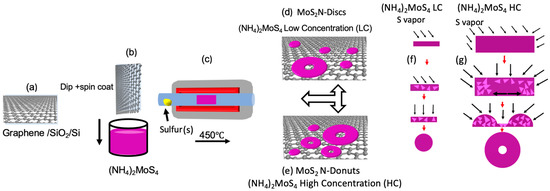
Figure 1.
Schematic description of the synthesis process (a) graphene transferred on SiO2/Si substrates via a wet transfer procedure (b,c) MoS2 on graphene using the vapor transport process. (d) synthesis of the MoS2 N-Discs with low concentrations of (NH4)2MoS4 precursor solution and (e) synthesis of the MoS2 N-donuts with high concentrations of (NH4)2MoS4 precursor solution. The hypothetical growth mechanism MoS2 N-discs at low (f) and MoS2 N-Donuts at high (g) (NH4)2MoS4 precursor concentration, respectively. Triangles represent MoS2 nuclei formed during the vapor transport annealing process.
Figure S1a exhibits the Raman spectra taken on three samples including the pristine graphene (green, inset), MoS2/graphene nanohybrids made with 0.10 wt% precursor concentration (red, with MoS2 N-discs dominant) and with 0.26 wt% precursor concentration (blue, MoS2 N-donuts dominant) (Supporting Information). The graphene’s G peak at ~1600 cm−1 due to the primary in-plane vibration mode and 2D peak at ~2707 cm−1 due to secondary in-plane vibration of zone-boundary phonons [50], and D peak at ~1356 cm−1 (associated with the defect in graphene8) are clearly observable on these samples. On the pristine graphene, the intensity ratio of 2D to G peak (I2D/IG) is around 1.8 while ID/IG is negligible, indicating that the graphene is a monolayer with high quality. On the MoS2/graphene nanohybrid made with 0.10 wt% precursor concentration, the graphene’s Raman peak intensities are notably enhanced most probably due to the LSPR effect by the MoS2 nanostructures [26]. The enhancement factor of the graphene G peak is ~5. Interestingly, a higher enhancement factor of ~8 can be observed on the graphene G peak of the MoS2/graphene nanohybrid sample made with 0.26 wt% precursor concentration, indicating a stronger LSPR effect. It should be noted that such an enhancement in the Raman signatures of graphene by metallic plasmonic nanostructures has been reported on metal-nanostructures/graphene nanohybrid samples [13,51,52]. A similar enhancement observed on MoS2/graphene nanohybrids indicates that the LSPR can be effectively generated on nonmetallic TMD nanostructures. Figure S1b displays the Raman spectra of MoS2 taken on the MoS2/graphene nanohybrids made with 0.10 wt% (red) and 0.26 wt% (blue) precursor concentrations, respectively, using Raman excitation at 488 nm. The Raman peaks in both spectra can be indexed to the at ~393 cm−1 (due to S and Mo atoms in-plane displacement mode) and at ~419 cm−1 (due to the S atoms out of displacement mode) of MoS2 [53], confirming MoS2 was grown on graphene in the MoS2/graphene nanohybrid samples.
Figure 2a–f show Raman maps of MoS2 Ag1 peak taken on the MoS2/graphene nanohybrid samples made with different precursor solution concentrations of (a) 0.06 wt %, (b) 0.10 wt %, (c) 0.2 wt %, (d) 0.26 wt %, (e) 0.32 wt%, and (f) 0.40 wt%. The Raman maps show that the MoS2 formed is not in a continuous layer, rather in the morphology of NPs of approximately round shape in the selected (NH4)2MoS4 precursor concentration range. Quantitatively, the (NH4)2MoS4 precursor concentration exhibits an effect on both the MoS2 NP density and shape. At the lowest precursor concentration of 0.06 wt%, the round shape of MoS2 NPs grows in two different sizes: smaller size with an average diameter of ~200 nm (majority) and larger size with an average diameter of ~1.0 µm with low density. With increasing precursor concentrations in the range of 0.20–0.26 wt%, the size of the MoS2 NPs changes moderately in the range of 300–600 nm, while the NP density increases. Above the precursor concentration of 0.26 wt%, the lateral dimension of the MoS2 NPs increases considerably and the NP density decreases.
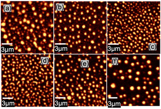
Figure 2.
MoS2 Ag1 peak Raman maps of MoS2 N-donuts and N-discs/graphene samples that were synthesized with different precursor solution concentrations of (a) 0.06 wt%, (b) 0.10 wt%, (c) 0.20 wt%, (d) 0.26 wt%, (e) % 0.32 wt%, and (f) % 0.40 wt%.
A more quantitative measurement of the morphology and density of the MoS2 NPs is shown in Figure 3 and Figure 4 at different precursor concentrations using AFM. The discontinuous morphologies of the MoS2 NPs have been confirmed in the entire range of the precursor concentration (Figure 3) and the result agrees well qualitatively with the Raman maps in Figure 2. However, the better spatial resolution in AFM images in Figure 3 suggests the MoS2 NPs tend to have irregular shapes at lower precursor concentrations while becoming more round-shaped at higher precursor concentrations of 0.26 wt% or higher.
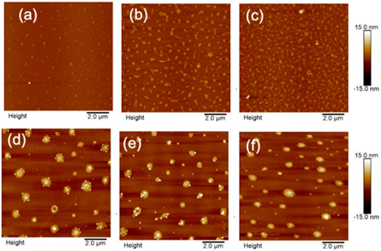
Figure 3.
Contact mode AFM images (10 µm × 10 µm) of MoS2 samples that were synthesized with different precursor solution concentration. (a) 0.06 wt%, (b) 0.10 wt %, (c) 0.20 wt%, (d) 0.26 wt%, (e) 0.32 wt%, and (f) 0.40 wt%.
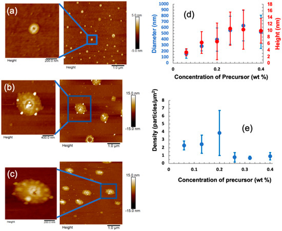
Figure 4.
(a–c) Representative contact AFM images (5 µm × 5 µm) along with images of individual features from samples synthesized from MoS2 precursor concentrations of (a) 0.06 wt% (b) 0.26 wt% and (c) 0.40 wt% with zoom in. (d) Average diameter (blue) and height (red) of MoS2 NPs as a function of precursor concentration. (e) Average density of MoS2 NPs as a function of precursor concentration. Error bars represent the standard deviation of the measurement.
AFM images of 5 µm × 5 µm at selected concentrations of 0.06 wt%, 0.26 wt%, and 0.40 wt% are shown in Figure 4a–c along with zoomed-in images of single MoS2 N-donuts and N-discs features. Interestingly, MoS2 N-discs of smaller lateral dimensions are the dominant features at lower precursor concentrations. In contrast, MoS2 N-donuts have a larger lateral dimension and are present even in samples made at the lowest precursor concentration of 0.06 wt%. With increasing precursor concentration, the proportion of the MoS2 N-donuts increases, and in the samples made with precursor concentrations of 0.26% or higher, MoS2 N-donuts become the dominant features. The average dimensions and density of the features are shown in Figure 4d,e as a function of the precursor concentration. At low precursor concentrations, the MoS2 NP diameter is between 200 to 400 nm, the height is 2–7 nm, and the density is 2–4 particles/µm2. Diameters and height increase up to 600 nm and 10 nm, respectively, with increasing precursor concentration which results in NP density decreasing to 1.5 to 1.0 particles/µm2. As shown in Figure 4d, the average diameter of the N-discs and N-donuts increases monotonically with the (NH4)2MoS4 precursor concentration from ~200 nm at 0.06 wt% precursor concentration to 600 nm at 0.26 wt% concentration. However, the average diameter seems to saturate at higher precursor concentrations.
Figure 5a displays the comparison of the Raman spectra of R6G (5 × 10⁻⁵ M) probe molecules on MoS2/graphene nanohybride substrates that were synthesized with different precursor solution concentrations from 0.06 wt% to 0.32 wt%, measured using the same excitation of 532 nm wavelength. Most of the R6G Raman peaks are visible on all spectra. Especially, the spectra include the R6G fundamental peaks at 613 cm−1 allocated to the C–C–C ring in-plane vibration mode, 773 cm−1 assigned to aromatic C–H bending mode, 1190 cm−1 and 1648 cm−1 allocated to C–O–C stretching mode and the C–C stretching mode, respectively [20,54]. Among the five spectra, the R6G spectra on the lowest precursor concentration of 0.06 wt% (green) have the lowest R6G peak intensity, indicative of the lowest SERS enhancement. It should be mentioned that MoS2 N-discs are predominant in this sample. In contrast, the highest SERS enhancement is observed on the spectrum for MoS2/graphene nanohybride made with 0.26 wt% precursor concentration (black) on which MoS2 N-donuts are predominant. Quantitatively, the enhancement factor can be estimated using the ratio of the intensity of the R6G Raman peaks on the MoS2/graphene samples made using different precursor concentrations at 613 cm−1 and 773 cm−1 to the ones on the MoS2 (0.06 wt%)/graphene). Figure 5b exhibits the estimated enhancement factor as a function of precursor concentration of the five samples shown in Figure 5a. The maximum enhancement factor of 8.2 was obtained on the MoS2/graphene sample at 0.26 wt% precursor concentration, suggesting that the SERS enhancement is a compromise of the shape, dimension, and density of MoS2 NPs. Interestingly, MoS2 N-donuts are predominant in MoS2/graphene nanohybrides when the precursor concentration is exceeding ~0.20 wt%. The higher SERS sensitivity in this precursor concentration range, especially the peak SERS sensitivity in MoS2/graphene nanohybride made from 0.26 wt% precursor concentration, suggests that MoS2 N-donuts may support LSPR in a more preferable way than other N-discs or other shapes of MoS2 nanostructures.
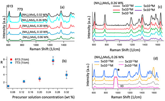
Figure 5.
(a) Average Raman spectra of R6G molecules at the concentration of 5 × 10⁻⁵ M, collected from six batches of the samples shown in Figure S2, deposited on five MoS2/graphene nanohybrids substrates, MoS2 was synthesized with a precursor solution concentration of 0.06 wt% to 0.32 wt%. (b) The corresponding enhancement factor of the 613 and 773 cm−1 R6G peaks intensity on the five samples that were synthesized with different precursor solution concentrations with respect to the one was synthesized with a precursor solution concentration of 0.06 wt%. (c,d) Raman spectra of the R6G molecules with different concentrations in the range of 5 × 10⁻⁵ M to 5 × 10⁻⁹ M (c), and 5 × 10⁻¹⁰ M to 2 × 10⁻¹² M (multiplied by 3) (d) on the MoS2/graphene nanohybrids substrates, MoS2 was synthesized with a precursor solution concentration of 0.26 wt%. The * mark denotes the Si peak.
The R6G molecule droplets of varying concentrations ranging from 5 × 10⁻⁵ M to 2 × 10⁻¹² M were cast and dried on the substrate and then Raman spectra were gathered with a 532 nm laser. The R6G Raman spectra are compared at the R6G concentrations of 5 × 10⁻⁵ M to 5 × 10⁻⁹ M in Figure 5c, and the R6G concentrations of 5 × 10⁻¹⁰ M to 2 × 10⁻¹² M in Figure 5d, respectively. All Raman signatures peaks of R6G are obvious at R6G concentrations above 5 × 10⁻¹⁰ M. With further reduction of the R6G concentration to 2 × 10⁻¹² M, most of the R6G Raman signature peaks are still detectable, particularly the vibrational modes with larger polarizability, such as 613 cm−1, 773 cm−1, 1191 cm−1, and 1648 cm−1. Therefore, the R6G sensitivity of 2 × 10⁻¹² M on the MoS2 N-donuts/graphene nanohybrid is about half an order of magnitude higher than that obtained on MoS2 N-discs/graphene [26] and about one order of magnitude higher than the best so far reported using the plasmonic metal nanostructure/graphene substrates [17].
Figure 6 shows the comparison of SERS Sensitivity and R6G 613 cm−1 peak enhancement factor (normalized with respect to that on graphene only SERS substrates) on different SERS substrates of graphene only, MoS2 N-discs/graphene [26], AuNPs+MoS2 N-discs (0.10 wt%)/graphene [29], WS2 N-discs+MoS2 N-discs (0.10 wt%)/graphene [55] and MoS2 N-donuts/graphene (made from 0.26 wt% precursor concentration in this work). The result shows that the best enhancement was obtained on the MoS2 N-donuts/graphene.
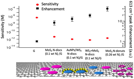
Figure 6.
Comparison of SERS Sensitivity and R6G 613cm−1 peak enhancement on different SERS substrates: graphene, MoS2 N-discs (0.10 wt%)/graphene, AuNPs/MoS2 N-discs (0.10 wt%)/graphene, WS2 N-discs +MoS2 N-discs (0.10 wt%)/graphene and MoS2 N-donuts (0.26 wt%)/graphene.
The R6G Raman peak intensities at 613 cm−1 and 773 cm−1 as a function of the R6G concentration are depicted in Figure S3a–d for the MoS2 (0.26 wt%)/graphene. Figure S3a,b are in linear scale while Figure S3c,d, in semi-logarithmic scale. The curves can be fitted approximately with an equation of as shown in Figure S3. Indeed, this logarithmic relation between the SERS intensity and concentration is noted in earlier reports of SERS sensitivity on a variety of analyte molecules [15,19,56,57].
The experimental results presented in this paper suggest a higher field enhancement for the case of TMD nanodonuts which may also depend on the details of the size and shape of the particles. The focus of our simulations is to examine the plasmonic features of such nanostructures and their differences with NDs. For this, we adopted a phenomenological approach that can reveal these issues without dealing with the detailed microscopic treatment of plasmonic features of the TMD NDs and nanodonuts, which is out of our current scope. For this, we chose Ag as a material model. Of course, such a material structure is very different from the MoS2 material studied in this paper. However, since LSPRs are ubiquitous optical signatures of charge carriers, as shown below, our model can explain the impact of the shapes of MoS2 structures studied in this paper on the SERS enhancement. The simulations were done considering a normal planar polarized light reaching an NDs or N-donut placed on a SiO2 substrate (Figure 1). The substrates were considered to be air. The mesh size in the x–y plane is considered to be 4 nm and along the z-axis 0.5 nm. The extinction spectra of the structures were obtained as 1-T, wherein T was the transmittance.
To further clarify the impact of structure, we considered Ag N-donuts with external diameters (D) of 500, 360, and 240 nm (Figure 7a). The thicknesses were considered to be about 10 nm based on the experiment. The results presented in Figure 7b show the plasmonic bi-resonance nature of such N-donuts. When the external diameter of the N-donuts is 500 nm, these resonances occur at 815 and 1833 nm (Figure 7b, solid line). As the diameter decreases both of these resonances are blue-shifted while they become more distinct (Figure 7b, dashed and dashed-dotted lines).
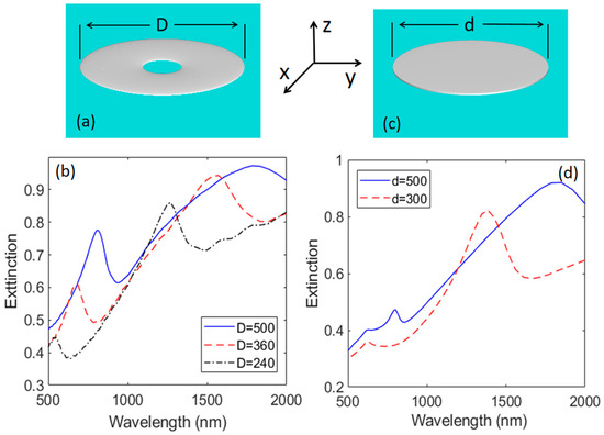
Figure 7.
(a) Simulation structural model of an Ag N-donut with an external diameter of D. (b) Extinction of Ag N-donuts with D = 500 (solid line), 360 (dashed line), and 240 nm (dashed-dotted line). (c) Simulation structural model of an Ag N-discs with diameter d. (d) Extinction spectra of the Ag N-discs with d = 500 (solid line) and 300 nm (dashed line). The thicknesses of the N-donuts are considered to be 10 nm and those of N-discs to be 7 nm.
The bi-resonance nature of N-donuts allows them to present a robust field enhancement over a wide range of wavelengths. To see this in Figure 8 we show the field enhancement profiles associated with the N-donuts with external diameters of 500 nm (a–d) and 240 nm (a’–d’). These results suggest that the shorter wavelength peaks seen in Figure 7b are associated with the inner openings of the N-donuts (inner modes). The field enhancement profiles of such modes in the x–y (Figure 8a) and x–z (Figure 8c) planes show high values around the inner edges of the N-donuts. As the wavelength increases, these modes are gradually transformed to the outer edge modes of the N-donuts (Figure 8b,d). The same scenario can also be seen for the case of N-donuts with an external diameter of 240 nm. As seen in Figure 8a’–d’ in this case the bi-resonance nature of plasmonic effects are more continuous, offering large plasmonic field enhancement over a wide range of wavelength. For both cases of D = 500 and 240 nm, around the wavelengths that the inner modes happen, the structures support some degree of optical field enhancement deep in the superstrate. For the near field, close to the surface of N-donuts, one expects a field enhancement factor of more than 4.
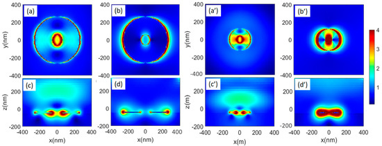
Figure 8.
Mode field enhancement profiles associated with the N-donuts with D = 500 nm (a–d) and 240 nm (a’–d’). (a,c) are the profiles in the x–y and x–z planes at 814 and (b,d) are those at 1833 nm. (a’,c’) are profiles at 532 nm and (b’,d’) are those at 1270 nm.
In the case of N-discs (Figure 7c), however, the prime feature of the plasmonic effect is associated with the dipolar nature of their edge modes. As seen in Figure 7d, in such a structure when the diameter is 500 or 300 nm, these modes happen at 1850 and 1385 nm, respectively. The weak peaks are seen at 800 and 620 nm could be associated with the weak cavity modes, generated by the relatively large lateral sizes of the N-discs. Figure S4 shows the mode field enhancement profiles in the x–y plane (Figure S4a,b) and the x–z plane (Figure S4c,d) when the diameter of the N-disc is 300 nm. Note that the field enhancement associated with cavity modes are rather weak. The dipolar-like mode is rather strong, but it happens in the infrared range.
4. Conclusions
In summary, we have developed a layer-by-layer growth process for the fabrication of MoS2 N-donuts/graphene nanohybrids SERS substrates. The MoS2 N-donuts growth process consists of two major steps: coating of (NH4)2MoS4 precursor at room temperature in air, followed by vapor transport anneal in sulfur vapor transfer process at 450 °C for 30 min. We have found that the predominant MoS2 N-donuts of the larger lateral dimension of 300–700 nm and height of 5–10 nm can be obtained by varying the precursor concentration to exceeding 0.20 wt% to promote nonuniform MoS2 conversion on larger precursor nuclei. This is in contrast to the formation of predominantly MoS2 N-discs of smaller lateral dimension at lower precursor concentrations down to 0.06 wt%. A SERS study using R6G probe molecules has shown that higher R6G SERS sensitivity has been observed on MoS2 N-donuts/graphene nanohybrid substrates than on the MoS2 N-discs/graphene ones. Specifically, the highest SERS sensitivity up to 2 × 10⁻¹² M has been achieved on the MoS2 N-donuts/graphene nanohybrid SERS substrates made using 0.26 wt% precursor concentration. This is a half order of magnitude higher than 5 × 10⁻¹² M on the MoS2 N-discs/graphene SERS substrates. FDTD simulation indicates that MoS2 N-donuts can better support LSPR than their MoS2 N-discs counterparts. This result illustrates the feasibility of tuning TMD nanostructure morphology for high-performance nonmetallic plasmonic nanohybrids for low-cost, large-scale applications in biosensing and other optoelectronics.
Supplementary Materials
The following are available online at https://www.mdpi.com/article/10.3390/bios11120477/s1, Figure S1: (a) Raman spectra of pristine graphene (green, inset), and 0.10 wt% MoS2N-donuts/graphene (red), and 0.26 wt% MoS2N-discs/graphene (blue). (b) Raman spectrum of MoS2N- donuts (0.26 wt%) and discs (0.10 wt%)/graphene. All spectra were taken using 488 n, Figure S2: The enhanced Raman spectra of the R6G molecules 5 × 10⁻⁵M deposited on five MoS2/graphene nanohybrids substrates, MoS2 was synthesized with a precursor solution concentration of 0.06 wt % (a), 0.10 wt %, 0.20 wt %, 0.26 wt %, and 0.32 wt % (e), the spectra were collected from six batches of MoS2 NDs/graphene substrates samples, Figure S3: The intensities of the Raman at 613 cm−1 peak as a function of the R6G concentration on substrates using a linear scale (a, b) and a semi-logarithmic scale (c,d). The Raman excitation was at 532 nm, Figure S4: Mode field enhancement profiles in x–y planes of an N-disk with D = 300 nm at 620 nm (a) and 1385 (b). (c) and (d) show, respectively, their profiles in the x–z planes.
Author Contributions
S.A.G. and J.Z.W. designed the experiment; S.A.G. prepared the samples; S.A.G. and C.L.B. did the sample characterization. S.M.S. participated in the simulation. S.A.G. and J.Z.W. led the effort in manuscript writing. All authors have read and agreed to the published version of the manuscript.
Funding
This work was supported by US Army Research Office Contract ARO-W911NF-16-1-0029 and National Science Foundation Contracts NSF-ECCS-1809293, and NSF-DMR-1909292.
Institutional Review Board Statement
Not applicable.
Informed Consent Statement
Not applicable.
Data Availability Statement
Not applicable.
Acknowledgments
The authors acknowledge support in part by US Army Research Office Contract ARO-W911NF-16-1-0029 and National Science Foundation Contracts NSF-ECCS-1809293/1809284 and NSF-DMR-1909292. SAG acknowledges the support from Jazan University.
Conflicts of Interest
The authors declare no conflict of interest.
References
- Fang, Y.; Seong, N.H.; Dlott, D.D. Measurement of the Distribution of Site Enhancements in Surface-Enhanced Raman Scattering. Science 2008, 321, 388–392. [Google Scholar] [CrossRef]
- Lin, H.X.; Li, J.M.; Liu, B.J.; Liu, D.Y.; Liu, J.; Terfort, A.; Xie, Z.X.; Tian, Z.Q.; Ren, B. Uniform Gold Spherical Particles for Single-Particle Surface-Enhanced Raman Spectroscopy. Phys. Chem. Chem. Phys. 2013, 15, 4130–4135. [Google Scholar] [CrossRef] [PubMed] [Green Version]
- Potara, M.; Baia, M.; Farcau, C.; Astilean, S. Chitosan-Coated Anisotropic Silver Nanoparticles as a SERS Substrate for Single-Molecule Detection. Nanotechnology 2012, 23, 055501. [Google Scholar] [CrossRef] [PubMed]
- Sivashanmugan, K.; Liao, J.D.; Liu, B.H.; Yao, C.K. Focused-Ion-Beam-Fabricated Au Nanorods Coupled with Ag Nanoparticles Used as Surface-Enhanced Raman Scattering-Active Substrate for Analyzing Trace Melamine Constituents in Solution. Anal. Chim. Acta 2013, 800, 56–64. [Google Scholar] [CrossRef]
- Guerrini, L.; Graham, D. Molecularly-Mediated Assemblies of Plasmonic Nanoparticles for Surface-Enhanced Raman Spectroscopy Applications. Chem. Soc. Rev. 2012, 41, 7085–7107. [Google Scholar] [CrossRef]
- Mu, C.; Zhang, J.P.; Xu, D. Au nanoparticle arrays with tunable particle gaps by template-assisted electroless deposition for high performance surface-enhanced Raman scattering. Nanotechnology 2010, 21, 015604. [Google Scholar] [CrossRef] [PubMed]
- Seo, S.; Chang, T.W.; Liu, G.L. 3D Plasmon Coupling Assisted Sers on Nanoparticle-Nanocup Array Hybrids. Sci. Rep. 2018, 8, 3002. [Google Scholar] [CrossRef] [Green Version]
- Xu, W.; Mao, N.; Zhang, J. Graphene: A Platform for Surface-Enhanced Raman Spectroscopy. Small 2013, 9, 1206–1224. [Google Scholar] [CrossRef]
- Ling, X.; Xie, L.; Fang, Y.; Xu, H.; Zhang, H.; Kong, J.; Dresselhaus, M.S.; Zhang, J.; Liu, Z. Can graphene be used as a substrate for Raman enhancement? Nano Lett. 2010, 10, 553–561. [Google Scholar] [CrossRef]
- Xu, W.; Ling, X.; Xiao, J.; Dresselhaus, M.S.; Kong, J.; Xu, H.; Liu, Z.; Zhang, J. Surface enhanced Raman spectroscopy on a flat graphene surface. Proc. Natl. Acad. Sci. USA 2012, 109, 9281–9286. [Google Scholar] [CrossRef] [Green Version]
- Geim, A.K.; Novoselov, K.S. The rise of graphene. Nat. Mater. 2007, 6, 183–191. [Google Scholar] [CrossRef]
- Geim, A.K.; Grigorieva, I.V. Van der Waals heterostructures. Nature 2013, 499, 419–425. [Google Scholar] [CrossRef]
- Lu, R.; Konzelmann, A.; Xu, F.; Gong, Y.; Liu, J.; Liu, Q.; Xin, M.; Hui, R.; Wu, J.Z. High Sensitivity Surface Enhanced Raman Spectroscopy of R6G on in Situ Fabricated Au Nanoparticle/Graphene Plasmonic Substrates. Carbon 2015, 86, 78–85. [Google Scholar] [CrossRef]
- Fan, W.; Lee, Y.H.; Pedireddy, S.; Zhang, Q.; Liu, T.; Ling, X.Y. Graphene oxide and shape-controlled silver nanoparticle hybrids for ultrasensitive single-particle surface-enhanced Raman scattering (SERS) sensing. Nanoscale 2014, 6, 4843–4851. [Google Scholar] [CrossRef]
- Goul, R.; Das, S.; Liu, Q.; Xin, M.; Lu, R.; Hui, R.; Wu, J.Z. Quantitative Analysis of Surface Enhanced Raman Spectroscopy of Rhodamine 6G Using a Composite Graphene and Plasmonic Au Nanoparticle Substrate. Carbon 2017, 111, 386–392. [Google Scholar] [CrossRef]
- Sun, H.-B.; Fu, C.; Xia, Y.-J.; Zhang, C.-W.; Du, J.-H.; Yang, W.-C.; Guo, P.-F.; Xu, J.-Q.; Wang, C.-L.; Jia, Y.-L.; et al. Enhanced Raman scattering of graphene by silver nanoparticles with different densities and locations. Mater. Res. Express 2017, 4, 025012. [Google Scholar] [CrossRef]
- Xu, S.; Jiang, S.; Wang, J.; Wei, J.; Yue, W.; Ma, Y. Graphene Isolated Au Nanoparticle Arrays with High Reproducibility for High-Performance Surface-Enhanced Raman Scattering. Sens. Actuator B Chem. 2016, 222, 1175–1183. [Google Scholar] [CrossRef]
- Yu, L.; Lu, L.; Zeng, L.; Yan, X.; Ren, X.; Wu, J.Z. Double Ag Nanowires on a Bilayer MoS2 Flake for Surface-Enhanced Raman Scattering. J. Phys. Chem. C 2021, 125, 1940–1946. [Google Scholar] [CrossRef]
- Xie, L.; Ling, X.; Fang, Y.; Zhang, J.; Liu, Z. Graphene as a substrate to suppress fluorescence in resonance Raman spectroscopy. J. Am. Chem. Soc. 2009, 131, 9890–9891. [Google Scholar] [CrossRef] [PubMed]
- Huh, S.; Park, J.; Kim, Y.S.; Kim, K.S.; Hong, B.H.; Nam, J.M. UV/ozone-Oxidized Large-Scale Graphene Platform with Large Chemical Enhancement in Surface-Enhanced Raman Scattering. ACS Nano 2011, 5, 9799–9806. [Google Scholar] [CrossRef]
- Zhang, Y.; Chang, T.R.; Zhou, B.; Cui, Y.T.; Yan, H.; Liu, Z.; Schmitt, F.; Lee, J.; Moore, R.; Chen, Y.; et al. Direct observation of the transition from indirect to direct bandgap in atomically thin epitaxial MoSe2. Nat. Nanotechnol. 2014, 9, 111–115. [Google Scholar] [CrossRef] [PubMed]
- Ling, X.; Fang, W.; Lee, Y.H.; Araujo, P.T.; Zhang, X.; Rodriguez-Nieva, J.F.; Lin, Y.; Zhang, J.; Kong, J.; Dresselhaus, M.S. Raman enhancement effect on two-dimensional layered materials: Graphene, h-BN and MoS2. Nano Lett. 2014, 14, 3033–3040. [Google Scholar] [CrossRef] [PubMed]
- Yin, Y.; Miao, P.; Zhang, Y.; Han, J.; Zhang, X.; Gong, Y.; Gu, L.; Xu, C.; Yao, T.; Xu, P.; et al. Significantly Increased Raman Enhancement on MoX2(X = S, Se) Monolayers upon Phase Transition. Adv. Funct. Mater. 2017, 27, 1606694. [Google Scholar] [CrossRef]
- Qiu, H.; Li, Z.; Gao, S.; Chen, P.; Zhang, C.; Jiang, S.; Xu, S.; Yang, C.; Li, H. Large-Area MoS2 Thin Layers Directly Synthesized on Pyramid-Si Substrate for Surface-Enhanced Raman Scattering. RSC Adv. 2015, 5, 83899–83905. [Google Scholar] [CrossRef]
- Xu, Y.Y.; Yang, C.; Jiang, S.Z.; Man, B.Y.; Liu, M.; Chen, C.S.; Zhang, C.; Sun, Z.C.; Qiu, H.W.; Li, H.S.; et al. Layer-controlled large area MoS2 layers grown on mica substrate for surface-enhanced Raman scattering. Appl. Surf. Sci. 2015, 357, 1708–1713. [Google Scholar] [CrossRef]
- Ghopry, S.A.; Alamri, M.A.; Goul, R.; Sakidja, R.; Wu, J.Z. Extraordinary Sensitivity of Surface-Enhanced Raman Spectroscopy of Molecules on MoS2 (WS2) Nanodomes/Graphene van der Waals Heterostructure Substrates. Adv. Opt. Mater. 2019, 7, 1801249. [Google Scholar] [CrossRef]
- Luther, J.M.; Jain, P.K.; Ewers, T.; Alivisatos, A.P. Localized surface plasmon resonances arising from free carriers in doped quantum dots. Nat. Mater. 2011, 10, 361–366. [Google Scholar] [CrossRef]
- Gong, M.; Sakidja, R.; Liu, Q.; Goul, R.; Ewing, D.; Casper, M.; Stramel, A.; Elliot, A.; Wu Judy, Z. Broadband Photodetectors Enabled by Localized Surface Plasmonic Resonance in Doped Iron Pyrite Nanocrystals. Adv. Opt. Mater. 2018, 6, 1701241. [Google Scholar] [CrossRef]
- Ghopry, S.A.; Alamri, M.; Goul, R.; Cook, B.; Sadeghi, S.M.; Gutha, R.R.; Sakidja, R.; Wu, J.Z. Au Nanoparticle/WS2 Nanodome/Graphene van der Waals Heterostructure Substrates for Surface-Enhanced Raman Spectroscopy. ACS Appl. Nano Mater. 2020, 3, 2354–2363. [Google Scholar] [CrossRef]
- Feng, S.; Dos Santos, M.C.; Carvalho, B.R.; Lv, R.; Li, Q.; Fujisawa, K.; Elias, A.L.; Lei, Y.; Perea-Lopez, N.; Endo, M.; et al. Ultrasensitive molecular sensor using N-doped graphene through enhanced Raman scattering. Sci. Adv. 2016, 2, e1600322. [Google Scholar] [CrossRef] [Green Version]
- Hong, S.; Li, X. Optimal Size of Gold Nanoparticles for Surface-Enhanced Raman Spectroscopy under Different Conditions. J. Nanomater. 2013, 2013, 49. [Google Scholar] [CrossRef]
- Yoon, J.K.; Kim, K.; Shin, K.S. Raman Scattering of 4-Aminobenzenethiol Sandwiched between Au Nanoparticles and a Macroscopically Smooth Au Substrate: Effect of Size of Au Nanoparticles. J. Phys. Chem. C 2009, 113, 1769–1774. [Google Scholar] [CrossRef]
- Mir-Simon, B.; Morla-Folch, J.; Gisbert-Quilis, P.; Pazos-Perez, N.; Xie, H.-n.; Bastús, N.G.; Puntes, V.; Alvarez-Puebla, R.A.; Guerrini, L. SERS efficiencies of micrometric polystyrene beads coated with gold and silver nanoparticles: The effect of nanoparticle size. J. Opt. 2015, 17, 114012. [Google Scholar] [CrossRef] [Green Version]
- Yoon, J.H.; Selbach, F.; Schumacher, L.; Jose, J.; Schlücker, S. Surface Plasmon Coupling in Dimers of Gold Nanoparticles: Experiment and Theory for Ideal (Spherical) and Nonideal (Faceted) Building Blocks. ACS Photonics 2019, 6, 642–648. [Google Scholar] [CrossRef]
- Stamplecoskie, K.G.; Scaiano, J.C.; Tiwari, V.S.; Anis, H. Optimal Size of Silver Nanoparticles for Surface-Enhanced Raman Spectroscopy. J. Phys. Chem. C 2011, 115, 1403–1409. [Google Scholar] [CrossRef]
- Makam, P.; Shilpa, R.; Kandjani, A.E.; Periasamy, S.R.; Sabri, Y.M.; Madhu, C.; Bhargava, S.K.; Govindaraju, T. SERS and fluorescence-based ultrasensitive detection of mercury in water. Biosens. Bioelectron. 2018, 100, 556–564. [Google Scholar] [CrossRef]
- Zhu, J.; Liu, M.J.; Li, J.J.; Li, X.; Zhao, J.W. Multi-branched gold nanostars with fractal structure for SERS detection of the pesticide thiram. Spectrochim. Acta Part A Mol. Biomol. Spectrosc. 2018, 189, 586–593. [Google Scholar] [CrossRef]
- Chen, X.; Nguyen, T.H.D.; Gu, L.; Lin, M. Use of Standing Gold Nanorods for Detection of Malachite Green and Crystal Violet in Fish by SERS. J. Food Sci. 2017, 82, 1640–1646. [Google Scholar] [CrossRef]
- Zhang, C.H.; Zhu, J.; Li, J.J.; Zhao, J.W. Small and Sharp Triangular Silver Nanoplates Synthesized Utilizing Tiny Triangular Nuclei and Their Excellent SERS Activity for Selective Detection of Thiram Residue in Soil. ACS Appl. Mater. Interfaces 2017, 9, 17387–17398. [Google Scholar] [CrossRef]
- Li, D.; Ma, Y.; Duan, H.; Deng, W.; Li, D. Griess reaction-based paper strip for colorimetric/fluorescent/SERS triple sensing of nitrite. Biosens. Bioelectron. 2018, 99, 389–398. [Google Scholar] [CrossRef]
- Li, Q.; Zhuo, X.; Li, S.; Ruan, Q.; Xu, Q.-H.; Wang, J. Production of Monodisperse Gold Nanobipyramids with Number Percentages Approaching 100% and Evaluation of Their Plasmonic Properties. Adv. Opt. Mater. 2015, 3, 801–812. [Google Scholar] [CrossRef]
- Alamri, M.; Sakidja, R.; Goul, R.; Ghopry, S.; Wu, J.Z. Plasmonic Au Nanoparticles on 2D MoS2/Graphene van der Waals Heterostructures for High-Sensitivity Surface-Enhanced Raman Spectroscopy. ACS Appl. Nano Mater. 2019, 2, 1412–1420. [Google Scholar] [CrossRef]
- Chen, P.X.; Qiu, H.W.; Xu, S.C.; Liu, X.Y.; Li, Z.; Hu, L.T.; Li, C.H.; Guo, J.; Jiang, S.Z.; Huo, Y.Y. A Novel Surface-Enhanced Raman Spectroscopy Substrate Based on a Large Area of MoS2 and Ag Nanoparticles Hybrid System. Appl. Surf. Sci. 2016, 375, 207–214. [Google Scholar] [CrossRef]
- Lu, Z.; Si, H.; Li, Z.; Yu, J.; Liu, Y.; Feng, D.; Zhang, C.; Yang, W.; Man, B.; Jiang, S. Sensitive, Reproducible, and Stable 3D Plasmonic Hybrids with Bilayer WS2 as Nanospacer for SERS Analysis. Opt. Express 2018, 26, 21626–21641. [Google Scholar] [CrossRef] [PubMed]
- Shorie, M.; Kumar, V.; Kaur, H.; Singh, K.; Tomer, V.K.; Sabherwal, P. Plasmonic DNA Hotspots Made from Tungsten Disulfide Nanosheets and Gold Nanoparticles for Ultrasensitive Aptamer-Based SERS Detection of Myoglobin. Mikrochim. Acta 2018, 185, 158. [Google Scholar] [CrossRef] [PubMed]
- Cook, B.; Liu, Q.; Liu, J.; Gong, M.; Ewing, D.; Casper, M.; Stramel, A.; Wu, J. Facile Zinc Oxide Nanowire Growth on Graphene via a Hydrothermal Floating Method: Towards Debye Length Radius Nanowires for Ultraviolet Photodetection. J. Mater. Chem. C 2017, 5, 10087–10093. [Google Scholar] [CrossRef]
- Gong, M.; Liu, Q.; Cook, B.; Kattel, B.; Wang, T.; Chan, W.L.; Ewing, D.; Casper, M.; Stramel, A.; Wu, J.Z. All-Printable ZnO Quantum Dots/Graphene van der Waals Heterostructures for Ultrasensitive Detection of Ultraviolet Light. ACS Nano 2017, 11, 4114–4123. [Google Scholar] [CrossRef]
- Xu, G.; Liu, J.; Wang, Q.; Hui, R.; Chen, Z.; Maroni, V.A.; Wu, J. Plasmonic graphene transparent conductors. Adv Mater 2012, 24, OP71–OP76. [Google Scholar] [CrossRef]
- Liu, Q.F.; Cook, B.; Gong, M.G.; Gong, Y.P.; Ewing, D.; Casper, M.; Stramel, A.; Wu, J.D. Printable Transfer-Free and Wafer-Size MoS2/Graphene van der Waals Heterostructures for High-Performance Photodetection. ACS Appl. Mater. Int. 2017, 9, 12728–12733. [Google Scholar] [CrossRef]
- Saito, R.; Hofmann, M.; Dresselhaus, G.; Jorio, A.; Dresselhaus, M.S. Raman spectroscopy of graphene and carbon nanotubes. Adv. Phys. 2011, 60, 413–550. [Google Scholar] [CrossRef]
- Mahigir, A.; Chang, T.W.; Behnam, A.; Liu, G.L.; Gartia, M.R.; Veronis, G. Plasmonic nanohole array for enhancing the SERS signal of a single layer of graphene in water. Sci. Rep. 2017, 7, 14044–14052. [Google Scholar] [CrossRef] [PubMed]
- Zhang, S.G.; Zhang, X.W.; Liu, X.; Yin, Z.G.; Wang, H.L.; Gao, H.L.; Zhao, Y.J. Raman Peak Enhancement and Shift of Few-Layer Graphene Induced by Plasmonic Coupling with Silver Nanoparticles. Appl. Phys. Lett. 2014, 104, 121109. [Google Scholar] [CrossRef]
- Lee, C.; Yan, H.; Brus, L.E.; Heinz, T.F.; Hone, J.; Ryu, S. Anomalous lattice vibrations of single- and few-layer MoS2. ACS Nano 2010, 4, 2695–2700. [Google Scholar] [CrossRef] [PubMed] [Green Version]
- Hou, M.-J.; Zhang, X.; Cui, X.-Y.; Liu, C.; Li, Z.-C.; Zhang, Z.-J. Preparation of SiO2@ Au nanorod array as novel surface enhanced Raman substrate for trace pollutants detection. Chin. Phys. B 2015, 24, 034203–034206. [Google Scholar] [CrossRef]
- Ghopry, S.A.; Sadeghi, S.M.; Farhat, Y.; Berrie, C.L.; Alamri, M.; Wu, J.Z. Intermixed WS2+MoS2 Nanodisks/Graphene van der Waals Heterostructures for Surface-Enhanced Raman Spectroscopy Sensing. ACS Appl. Nano Mater. 2021, 4, 2941–2951. [Google Scholar] [CrossRef]
- Li, M.; Zhang, J.; Suri, S.; Sooter, L.J.; Ma, D.; Wu, N. Detection of Adenosine Triphosphate with an Aptamer Biosensor based on Surface-Enhanced Raman Scattering. Anal. Chem. 2012, 84, 2837–2842. [Google Scholar] [CrossRef]
- Shi, Y.; Wang, H.; Jiang, X.; Sun, B.; Song, B.; Su, Y.; He, Y. Ultrasensitive, Specific, Recyclable, and Reproducible Detection of Lead Ions in Real Systems through a Polyadenine-Assisted, Surface-Enhanced Raman Scattering Silicon Chip. Anal. Chem. 2016, 88, 3723–3729. [Google Scholar] [CrossRef]
Publisher’s Note: MDPI stays neutral with regard to jurisdictional claims in published maps and institutional affiliations. |
© 2021 by the authors. Licensee MDPI, Basel, Switzerland. This article is an open access article distributed under the terms and conditions of the Creative Commons Attribution (CC BY) license (https://creativecommons.org/licenses/by/4.0/).