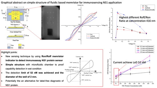
Fabrication and Characterization of Simple Structure Fluidic-Based Memristor for Immunosensing of NS1 Protein Application

 , , , , and
Abstract
1. Introduction
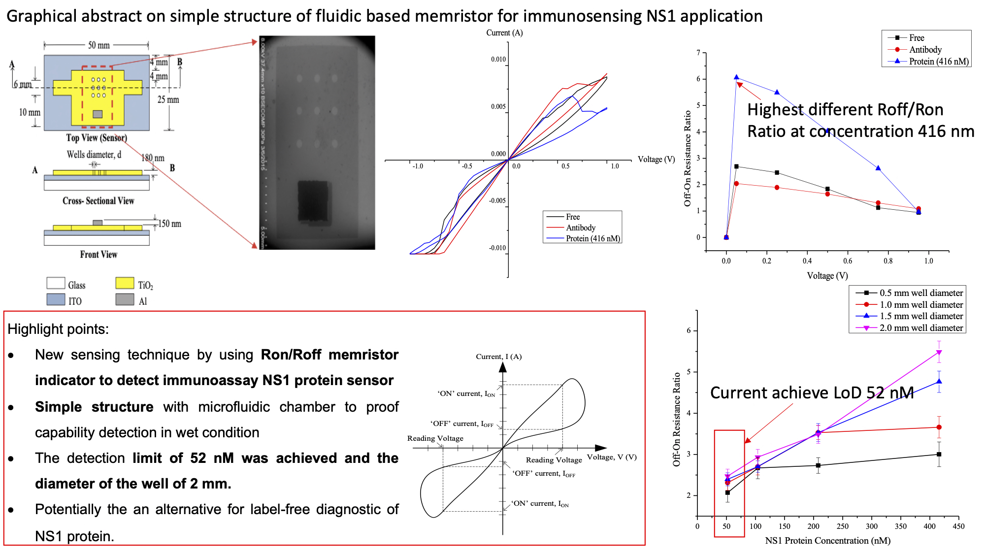
2. Sensing Principles
3. Methodology
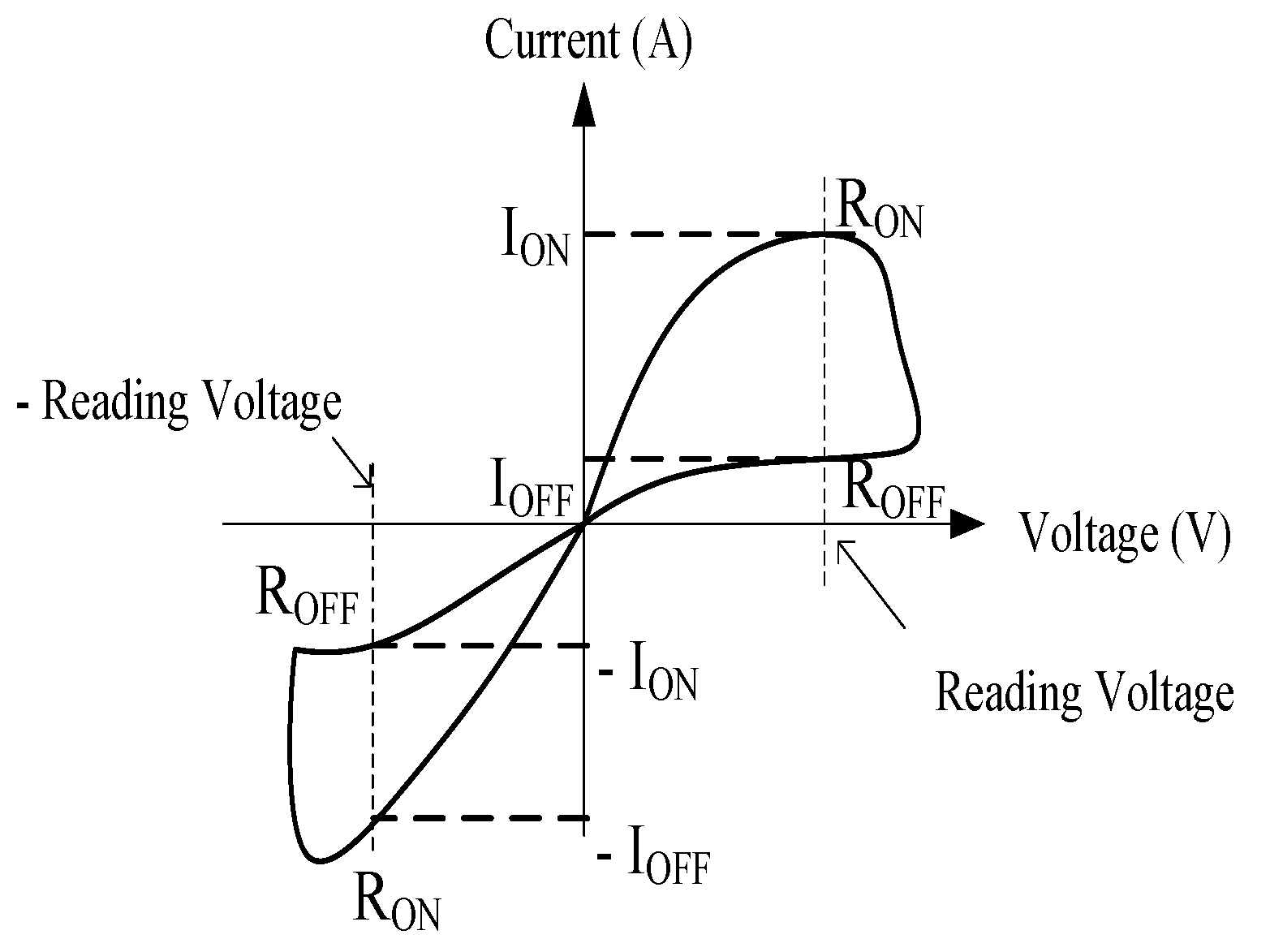
3.1. Sensor Development
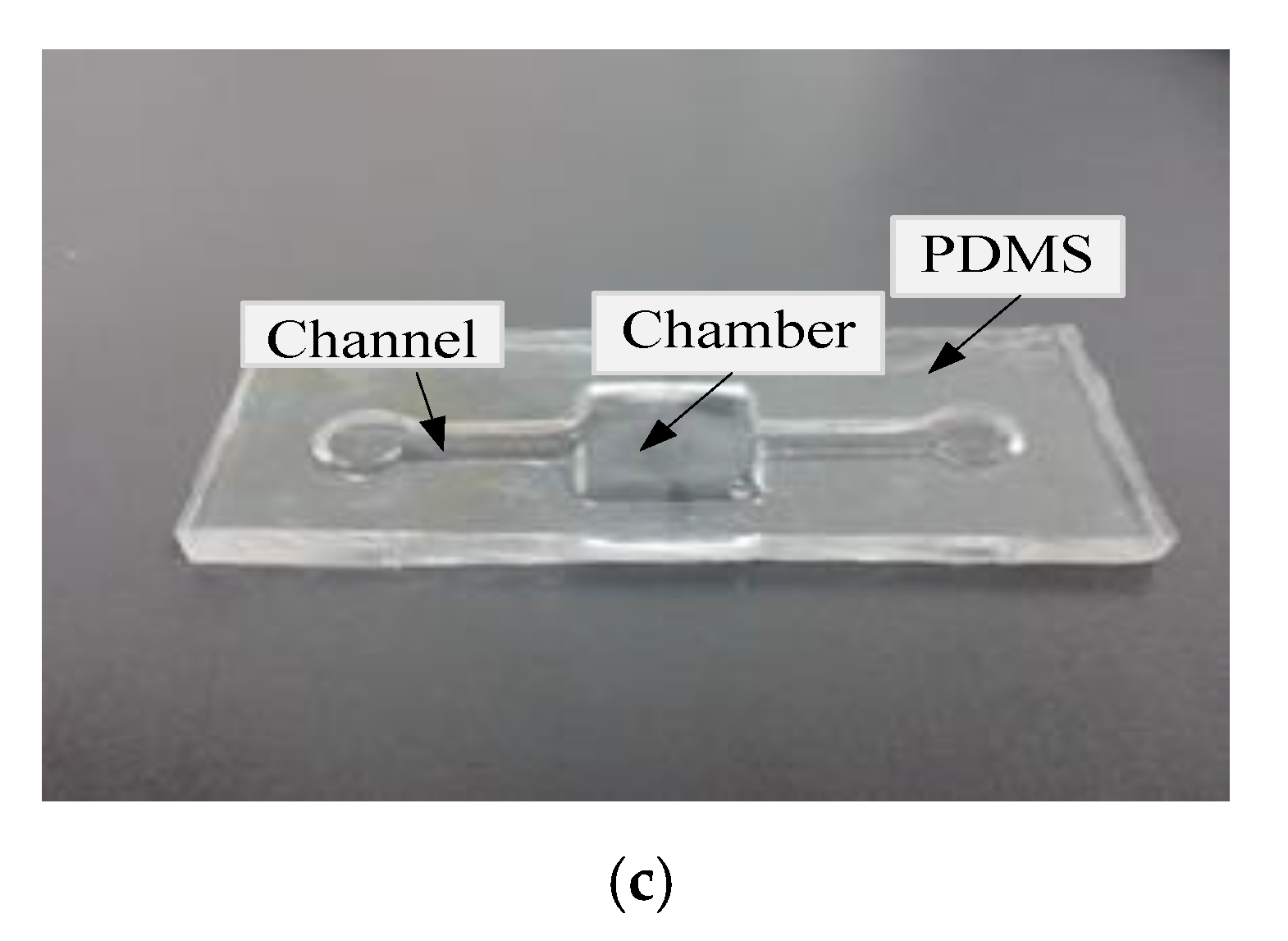
3.1.1. Microfludic Chamber
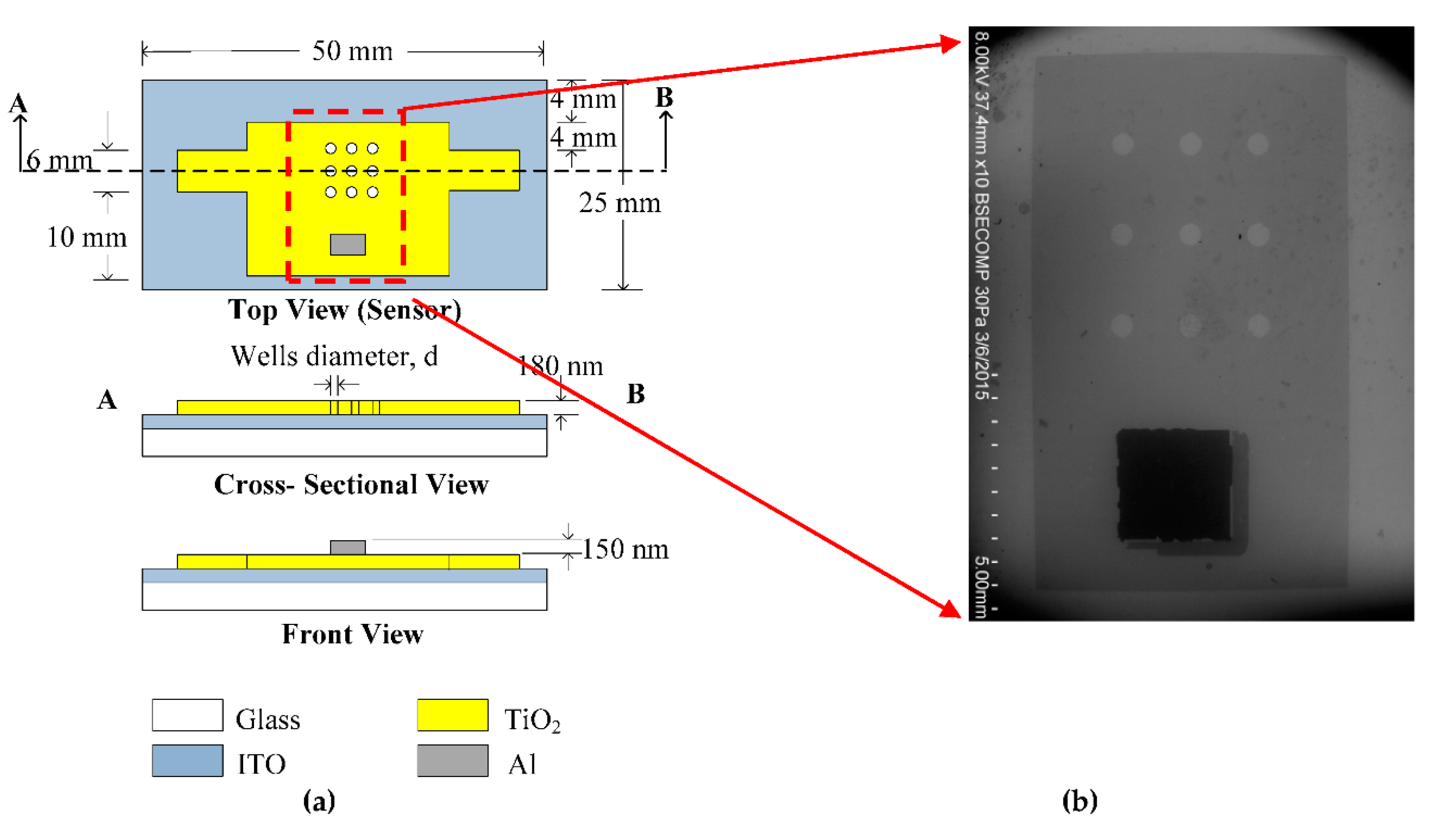
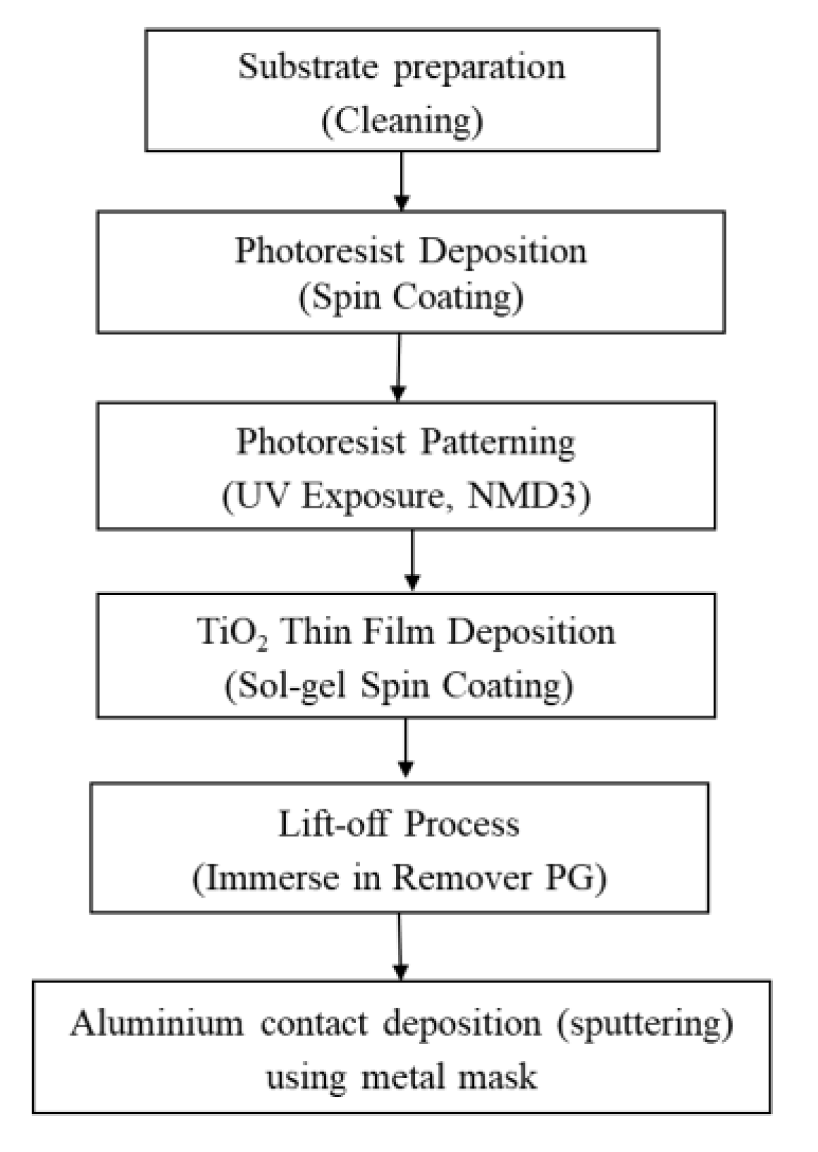
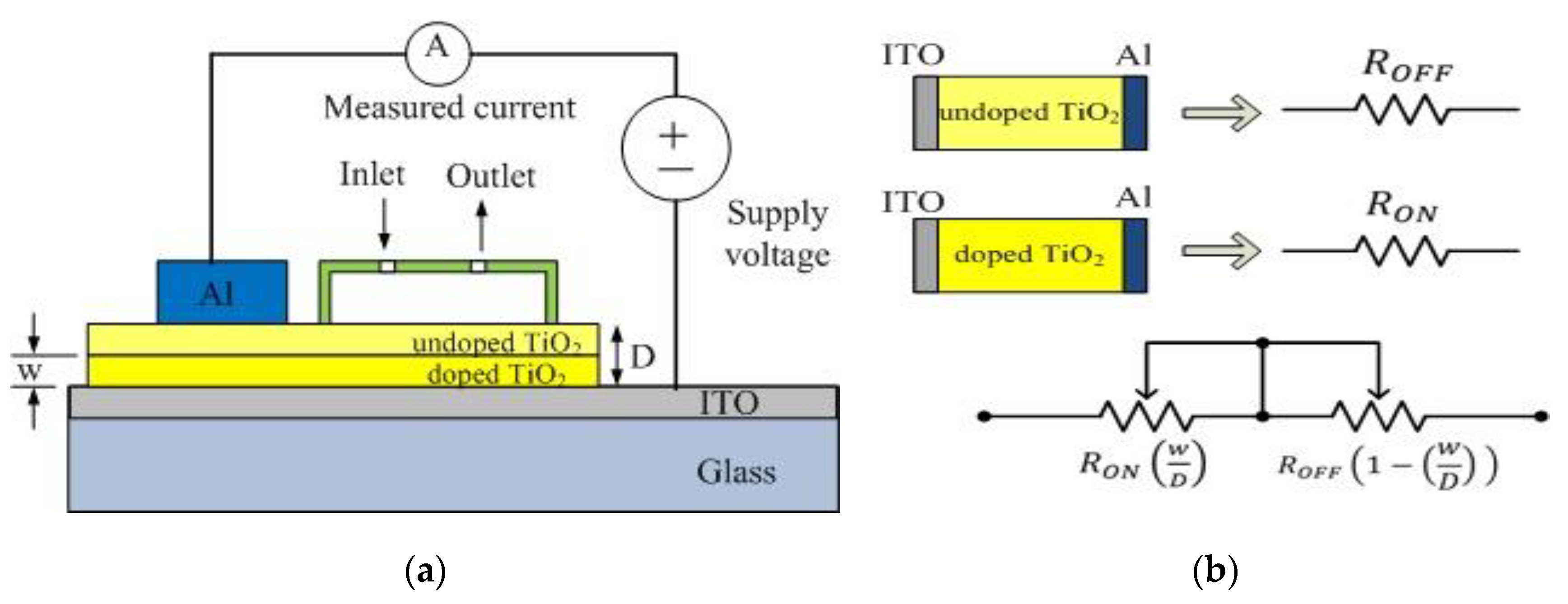
3.1.2. Sensing Platform
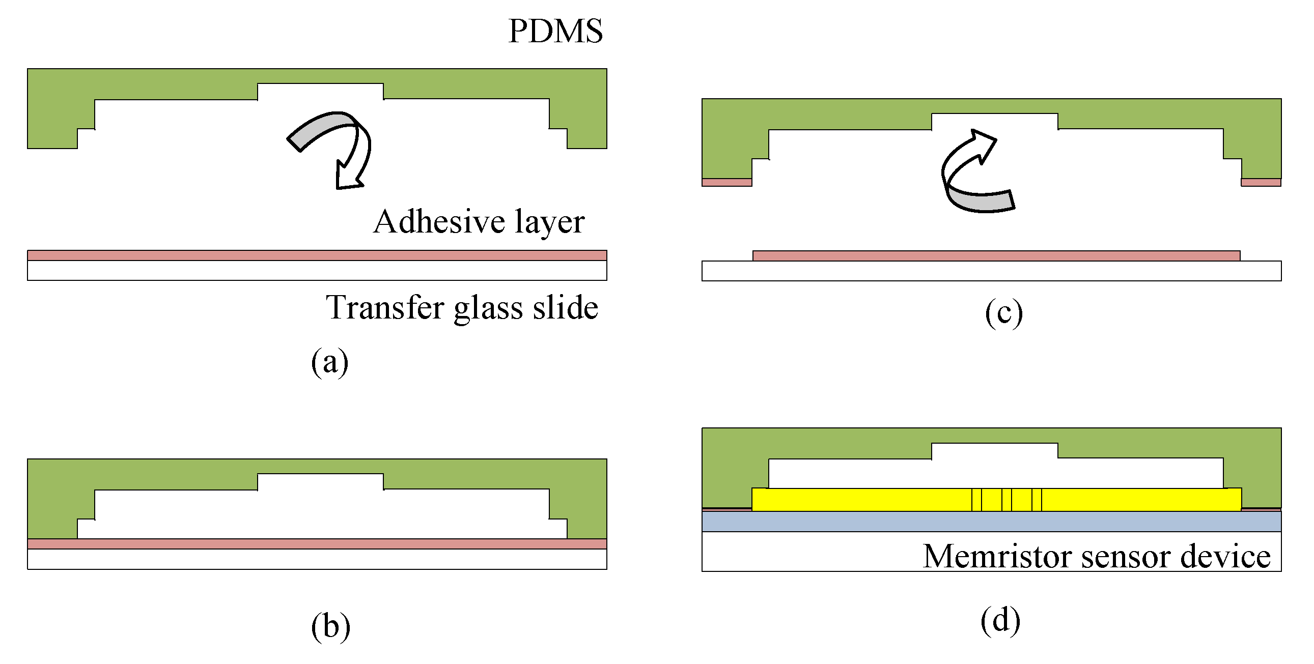
3.1.3. Sensor Bonding
3.2. Testing and Characterisations
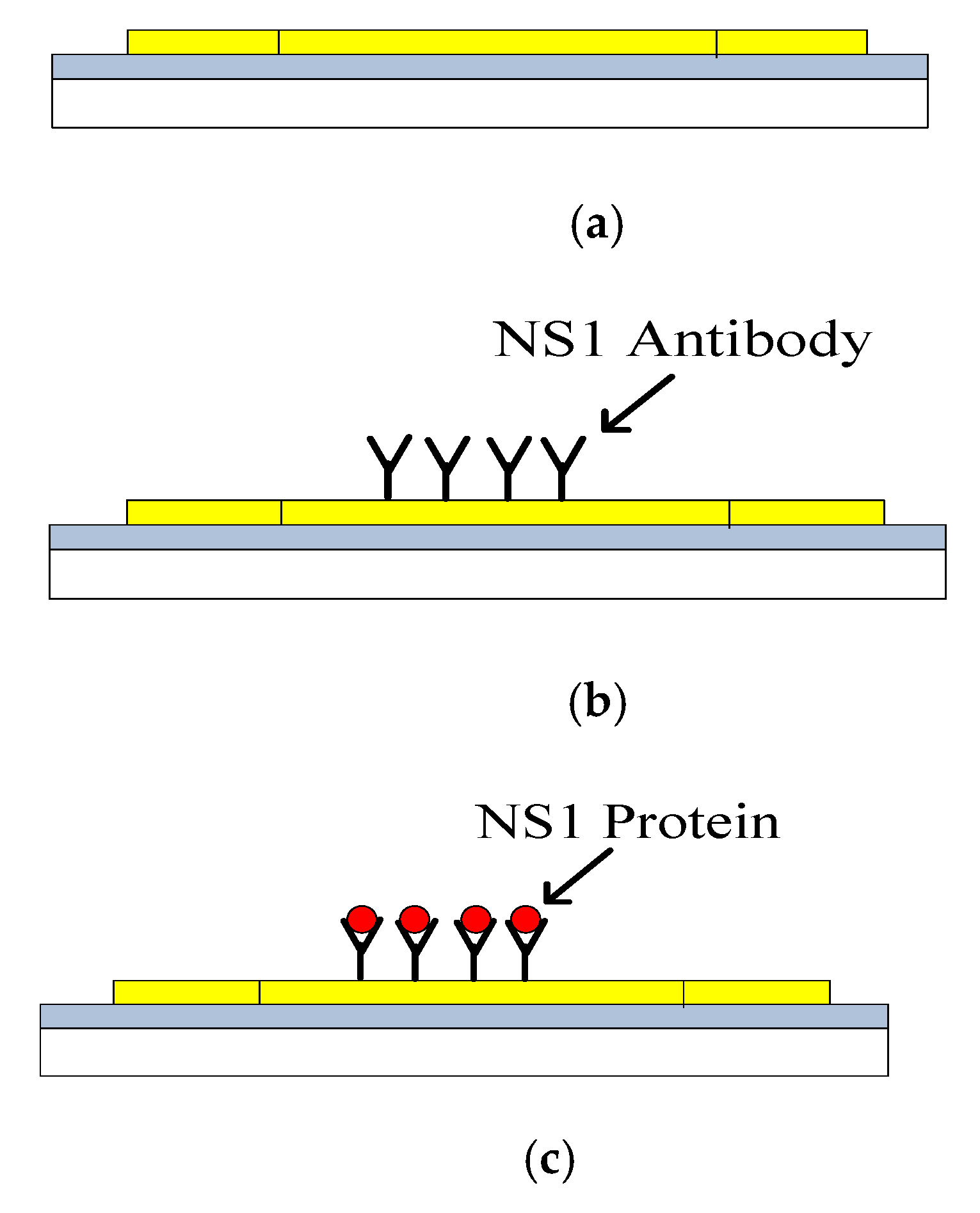
3.2.1. Surface Functionalisation and Sample Preparation
3.2.2. FESEM
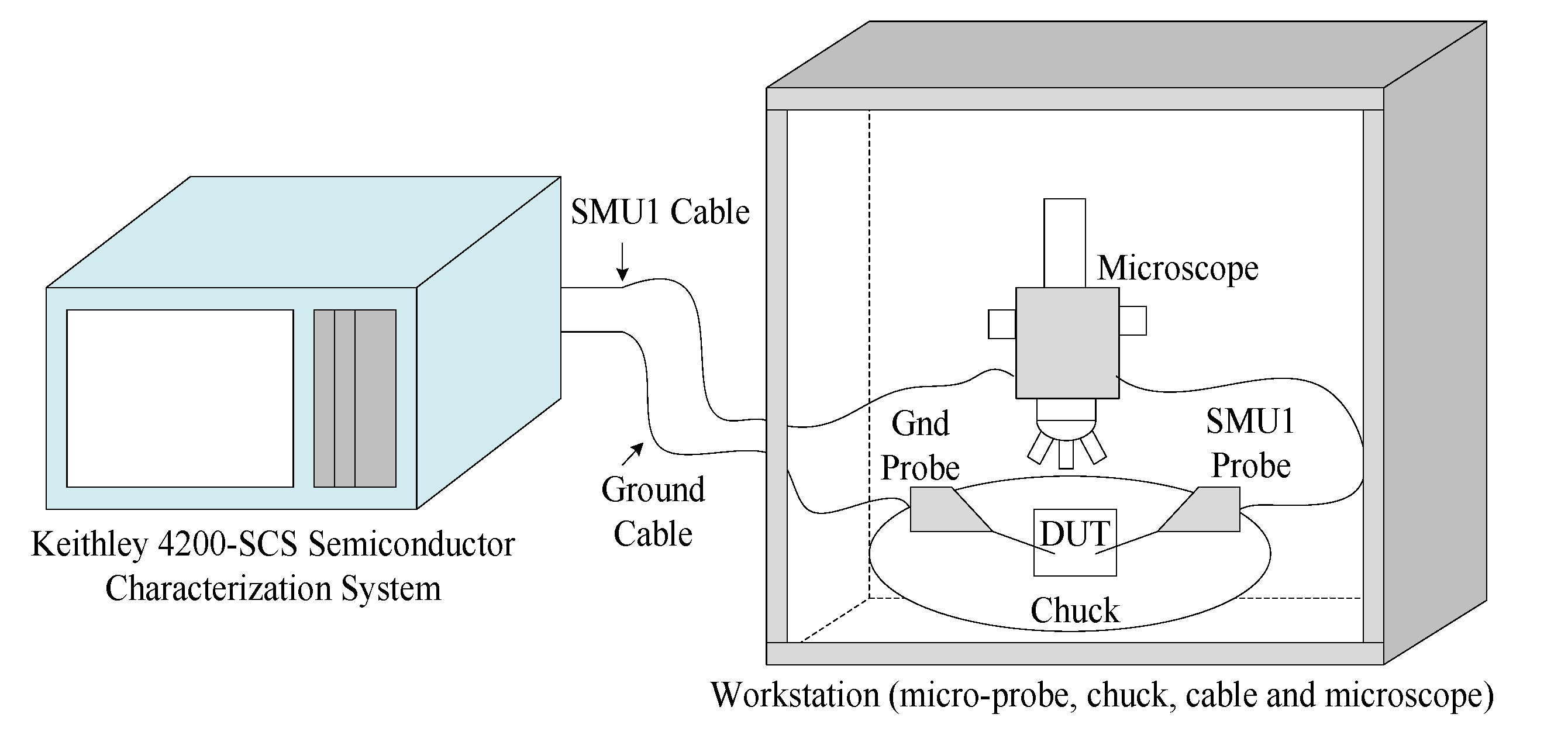
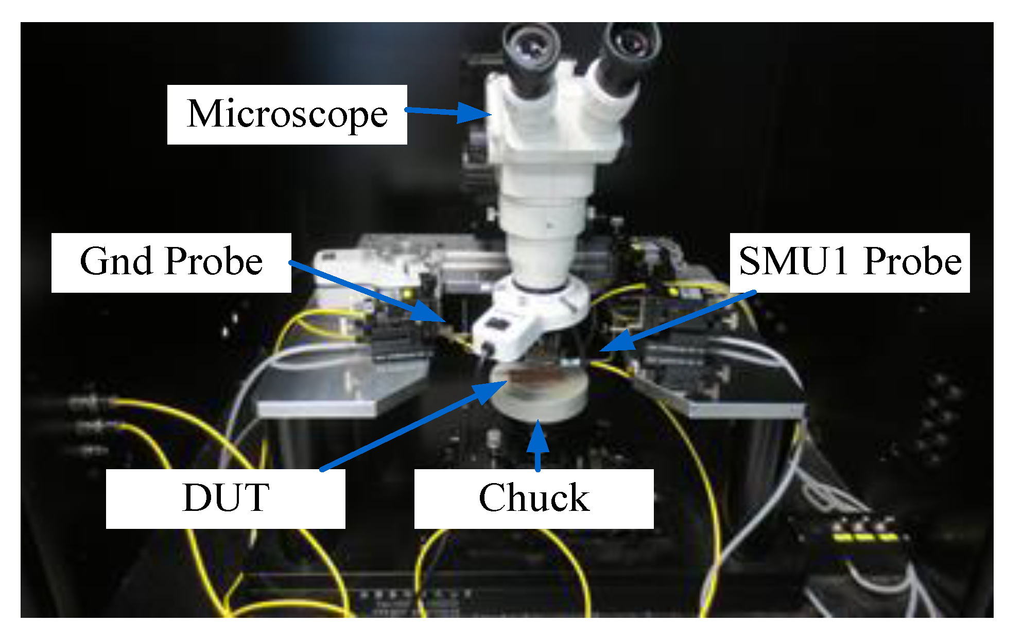
3.2.3. I-V Curve
3.3. Performance Measurements
4. Results and Discussions
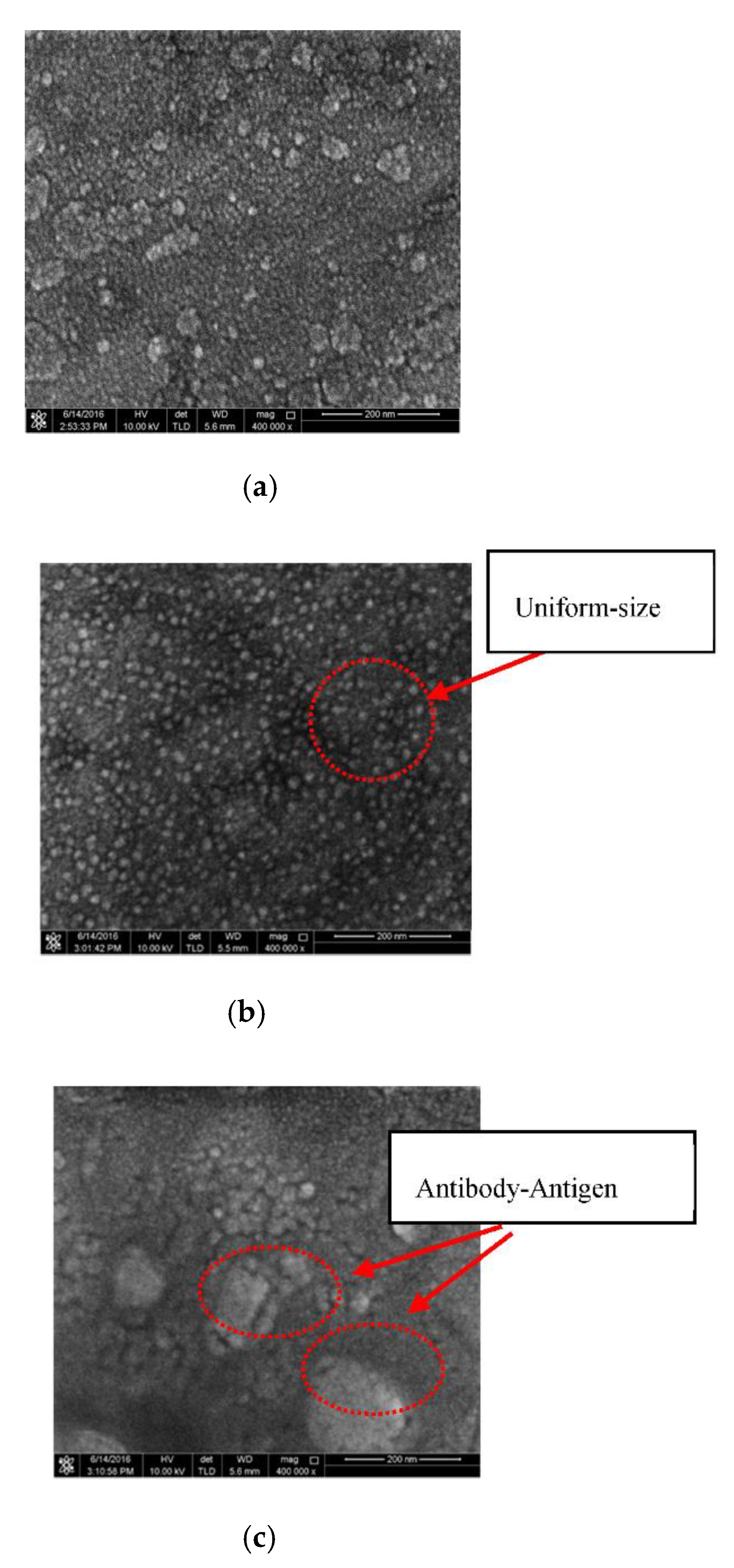
4.1. Surface Morphology
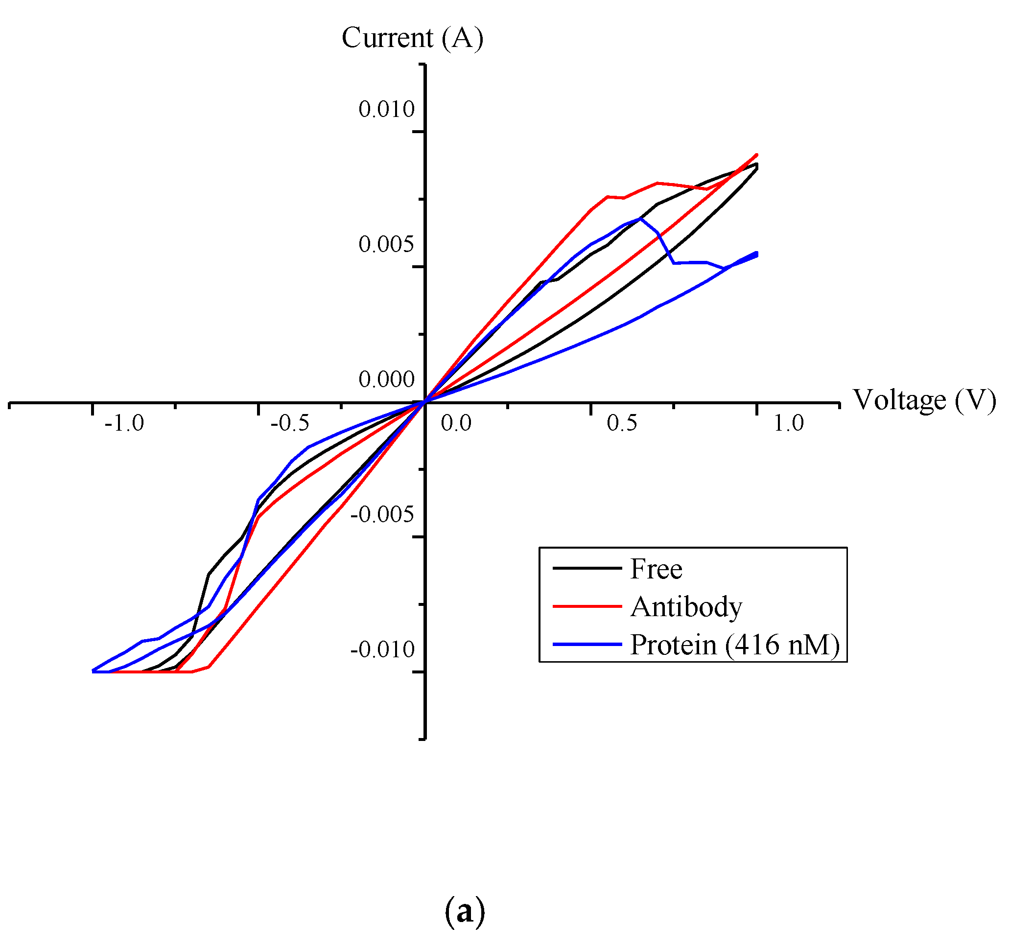
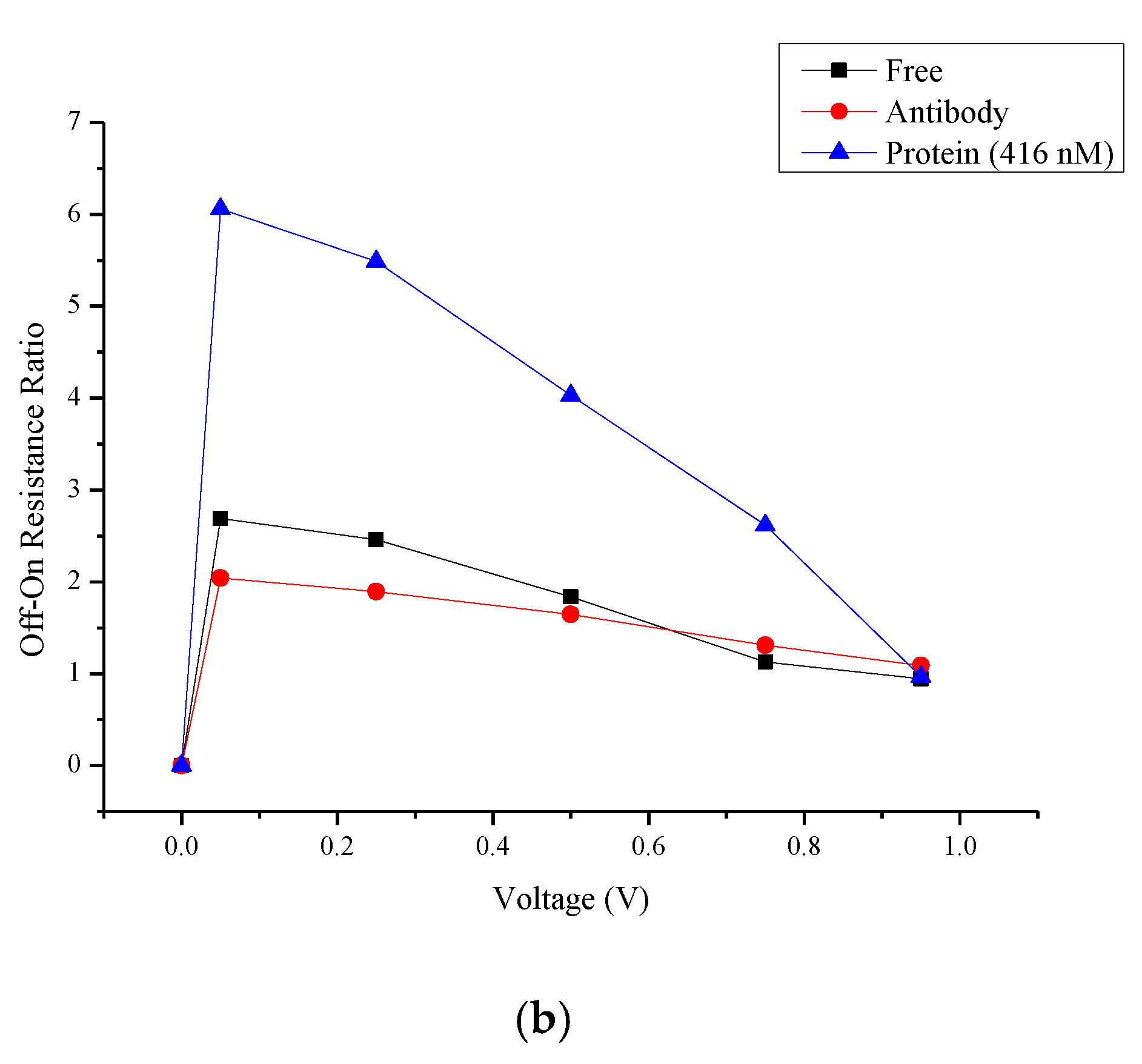
4.2. Hysteresis Loop Size and Resistance Ratio
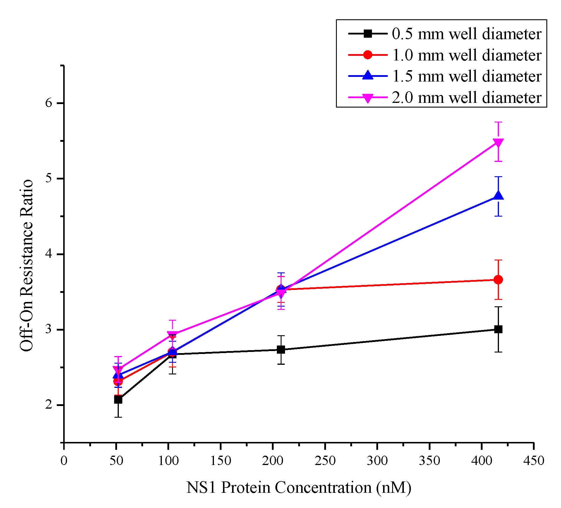
4.3. Sensitivity of Detection
5. Conclusions
Author Contributions
Funding
Acknowledgments
Conflicts of Interest
References
- Chua, L. Memristor-The missing circuit element. IEEE Trans. Circ. Theory 1971, 18, 507–519. [Google Scholar] [CrossRef]
- Strukov, D.B.; Snider, G.S.; Stewart, D.R.; Williams, R.S. The missing memristor found. Nat. Cell Biol. 2008, 453, 80–83. [Google Scholar] [CrossRef] [PubMed]
- Ho, Y.; Huang, G.M.; Li, P. Nonvolatile memristor memory. In Proceedings of the 2009 international conference on Multimodal interfaces—ICMI-MLMI ’09, Association for Computing Machinery (ACM), Cambridge, MA, USA, 2–4 November 2009. [Google Scholar]
- Wang, X.; Chen, Y.; Xi, H.; Li, H.; Dimitrov, D. Spintronic Memristor Through Spin-Torque-Induced Magnetization Motion. IEEE Electron. Dev. Lett. 2009, 30, 294–297. [Google Scholar] [CrossRef]
- Saifullah, M.S.M.; Subramanian, K.R.V.; Tapley, E.; Kang, D.J.; Welland, M.E.; Butler, M. Sub-10 nm Electron Beam Nanolithography Using Spin-Coatable TiO2Resists. Nano Lett. 2003, 3, 1587–1591. [Google Scholar] [CrossRef]
- Ganesan, R.; Dumond, J.; Saifullah, M.S.M.; Lim, S.H.; Hussain, H.; Low, H.Y. Direct Paterning of TiO2 Using Step-And-Flash Imprint Lithography. Acsnano 2012, 6, 1494–1502. [Google Scholar]
- Jo, S.H.; Chang, T.; Ebong, I.; Bhadviya, B.B.; Mazumder, P.; Lu, W. Nanoscale Memristor Device as Synapse in Neuromorphic Systems. Nanoletters 2010, 10, 5. [Google Scholar] [CrossRef] [PubMed]
- Yang, J.J.; Strukov, D.B.; Stewart, D.R. Memristive devices for computing. Nat. Nanotechnol. 2012, 8, 13–24. [Google Scholar] [CrossRef] [PubMed]
- Carrara, S.; Sacchetto, D.; Doucey, M.-A.; Baj-Rossi, C.; De Micheli, G.; Leblebici, Y. Memristive-biosensors: A new detection method by using nanofabricated memristors. Sens. Actuat. B Chem. 2012, 171, 449–457. [Google Scholar] [CrossRef]
- Puppo, F.; Dave, A.; Doucey, M.-A.; Sacchetto, D.; Baj-Rossi, C.; Leblebici, Y.; De Micheli, G.; Carrara, S. Memristive Biosensors Under Varying Humidity Conditions. IEEE Trans. NanoBiosci. 2014, 13, 19–30. [Google Scholar] [CrossRef] [PubMed]
- Tzouvadaki, I.; Parrozzani, C.; Gallotta, A.; De Micheli, G.; Carrara, S. Memristive Biosensors for PSA-IgM Detection. Bionanoscience 2015, 5, 189–195. [Google Scholar] [CrossRef]
- Wang, X.; Chen, Y.; Gu, Y.; Li, H. Spintronic Memristor Temperature Sensor. IEEE Electron. Dev. Lett. 2009, 31, 20–22. [Google Scholar] [CrossRef]
- Puppo, F.; Doucey, M.-A.; Di Ventra, M.; De Micheli, G.; Carrara, S. Memristor-based devices for sensing. In Proceedings of the 2014 IEEE International Symposium on Circuits and Systems (ISCAS), Melbourne, VIC, Australia, 1–5 June 2014; pp. 2257–2260. [Google Scholar]
- Hadis, N.S.M.; Manaf, A.A.; Herman, S.H.; Ngalim, S.H. ROFF/RON ratio of nano-well fluidic memristor sensor towards hydroxide based liquid detection. In Proceedings of the 2015 IEEE 15th International Conference on Nanotechnology (IEEE-NANO), Rome, Italy, 27–30 July 2015; pp. 1078–1081. [Google Scholar]
- Sun, H.; Wang, C.; Pang, S.; Li, X.; Tao, Y.; Tang, H.; Liu, M. Photocatalytic TiO2 films prepared by chemical vapor deposition at atmosphere pressure. J. Non-Cryst. Sol. 2008, 354, 1440–1443. [Google Scholar] [CrossRef]
- Wang, X.; Chen, Y.; Gibney, K.A.; Erramilli, S.; Mohanty, P. Silicon-based nanochannel glucose sensor. Appl. Phys. Lett. 2008, 92, 013903. [Google Scholar] [CrossRef]
- Patolsky, F.; Zheng, G.; Hayden, O.; Lakadamyali, M.; Zhuang, X.; Lieber, C.M. Electrical detection of single viruses. Proc. Natl. Acad. Sci. USA 2004, 101, 14017–14022. [Google Scholar] [CrossRef] [PubMed]
- Miller, K.J. Fabrication and Modeling of Thin-Film Anodic Titania Memristors. Master’s Thesis, Iowa State University, Ames, IA, USA, 2018. [Google Scholar]
- Kamarozaman, N.S.; Aznilinda, Z.; Herman, S.H.; Bakar, R.A.; Rusop, M. Effect of Annealing Duration on The Memristive Behavior of Pt/TiO2/ITO Memristive Device. In Proceedings of the 2012 IEEE International Confeference on Semiconductor. Electronics, Kuala Lumpur, Malaysia, 19–21 September 2012. [Google Scholar]
- Lin, Y.; Wu, G.; Yuan, X.Y.; Xie, T.; Zhang, L.D. Fabrication and optical properties of TiO2nanowire arrays made by sol gel electrophoresis deposition into anodic alumina membranes. J. Phys. Condens. Matter 2003, 15, 2917–2922. [Google Scholar] [CrossRef]
- Ettinger, A.; Wittmann, T. Fluorescence Live Cell Imaging. Met. Cell Biol. 2014, 123, 77–94. [Google Scholar]
- Camara, A.D.R.; Gouvêa, P.M.P.; Dias, A.C.M.S.; Braga, A.M.B.; Dutra, R.A.; De Araujo, R.E.; Carvalho, I.C.S. Dengue immunoassay with an LSPR fiber optic sensor. Opt. Expr. 2013, 21, 27023–27031. [Google Scholar] [CrossRef]
- Nayak, V.; Dessau, M.; Kucera, K.; Anthony, K.; Ledizet, M.; Modis, Y. Crystal Structure of Dengue Virus Type 1 Envelope Protein in the Postfusion Conformation and Its Implications for Membrane Fusion. J. Virol. 2009, 83, 4338–4344. [Google Scholar] [CrossRef]
- Gutsche, I.; Coulibaly, F.; Voss, J.E.; Salmon, J.; D’Alayer, J.; Ermonval, M.; Larquet, E.; Charneau, P.; Krey, T.; Mégret, F.; et al. Secreted dengue virus nonstructural protein NS1 is an atypical barrel-shaped high-density lipoprotein. Proc. Natl. Acad. Sci. USA 2011, 108, 8003–8008. [Google Scholar] [CrossRef]
- Gale, E.; Mayne, R.; Adamatzky, A.; Costello, B.D.L. Drop-coated titanium dioxide memristors. Mater. Chem. Phys. 2014, 143, 524–529. [Google Scholar] [CrossRef]
- Hadis, N.S.M.; Manaf, A.A.; Herman, S.H.; Ngalim, S.H. High Roff/Ron ratio liquid based memristor sensor using sol gel spin coating technique. In Proceedings of the 2015 IEEE SENSORS, Busan, Korea, 1–4 November 2015; pp. 1–4. [Google Scholar]
- Hadis, N.S.M.; Manaf, A.A.; Ngalim, S.H.; Herman, S.H.; Sawada, K.; Fauzi, N.A. Fabrication of fluidic-based memristor sensor for dengue virus detection. In Proceedings of the 2017 IEEE Asia Pacific Conference on Postgraduate Research in Microelectronics and Electronics (PrimeAsia), Kuala Lampur, Malaysia, 31 October–2 November 2017; pp. 105–108. [Google Scholar]


| Well-Diameter (mm) | Off-on Resistance Ratio |
|---|---|
| 0.5 | 3.25032 |
| 1.0 | 3.84784 |
| 1.5 | 4.77501 |
| 2.0 | 6.05929 |
| Wells Diameter (mm) | Sensitivity, S (nM)−1 |
|---|---|
| 0.5 | 2.06 × 10⁻³ |
| 1.0 | 3.58 × 10⁻³ |
| 1.5 | 6.57 × 10⁻³ |
| 2.0 | 8.21 × 10⁻³ |
Publisher’s Note: MDPI stays neutral with regard to jurisdictional claims in published maps and institutional affiliations. |
© 2020 by the authors. Licensee MDPI, Basel, Switzerland. This article is an open access article distributed under the terms and conditions of the Creative Commons Attribution (CC BY) license (http://creativecommons.org/licenses/by/4.0/).
Share and Cite
Mohamad Hadis, N.S.; Manaf, A.A.; Rahman, M.F.A.; Ngalim, S.H.; Hock Tang, T.; Citartan, M.; Ismail, A.; Herman, S.H. Fabrication and Characterization of Simple Structure Fluidic-Based Memristor for Immunosensing of NS1 Protein Application. Biosensors 2020, 10, 143. https://doi.org/10.3390/bios10100143
Mohamad Hadis NS, Manaf AA, Rahman MFA, Ngalim SH, Hock Tang T, Citartan M, Ismail A, Herman SH. Fabrication and Characterization of Simple Structure Fluidic-Based Memristor for Immunosensing of NS1 Protein Application. Biosensors. 2020; 10(10):143. https://doi.org/10.3390/bios10100143
Chicago/Turabian StyleMohamad Hadis, Nor Shahanim, Asrulnizam Abd Manaf, Mohamad Faizal Abd Rahman, Siti Hawa Ngalim, Thean Hock Tang, Marimuthu Citartan, Aziah Ismail, and Sukreen Hana Herman. 2020. "Fabrication and Characterization of Simple Structure Fluidic-Based Memristor for Immunosensing of NS1 Protein Application" Biosensors 10, no. 10: 143. https://doi.org/10.3390/bios10100143
APA StyleMohamad Hadis, N. S., Manaf, A. A., Rahman, M. F. A., Ngalim, S. H., Hock Tang, T., Citartan, M., Ismail, A., & Herman, S. H. (2020). Fabrication and Characterization of Simple Structure Fluidic-Based Memristor for Immunosensing of NS1 Protein Application. Biosensors, 10(10), 143. https://doi.org/10.3390/bios10100143