1. Introduction
The electrolyte–graphene interface plays a critical role in many promising applications of graphene, such as supercapacitors [
1,
2], biosensors [
3,
4], electrodes [
5], etc. It is, therefore, of considerable significance to have an accurate and more in-depth understanding of its properties. Of particular interest is its capacitance, which is a critical parameter that determines a device’s performance. The electrolyte–graphene interface can be modeled as two capacitors in series connection: the capacitance of the electrical double layer (EDL) and the quantum capacitance of graphene. Theoretical calculations indicate that the quantum capacitance of graphene dominates the total interfacial capacitance for few-layer graphene at low gating potentials, which originates from the low density of states (DOS) in graphene at low energy levels [
6,
7]. At potentials
V, the total capacitance is limited by the universal capacitance of the EDL due to the dielectric saturation of water and the steric effects of the ions at the electrolyte–graphene interface [
7]. Experimentally, Xia et al. [
8] first measured the electrolyte–graphene interfacial capacitance and extracted the quantum capacitance of graphene; the measured interfacial capacitance was shown as a V-shape dependence on gate voltage with a non-zero minimum at the Dirac point. Several other reports have recently demonstrated similar voltage-dependence of the interfacial capacitance of graphene in various electrolytes, such as ion-gels [
9] and aqueous electrolytes [
10,
11,
12].
These studies have revealed the voltage-dependence of the electrolyte–graphene interfacial capacitance; however, the measurements in most of these studies were performed at fixed frequencies, or within limited frequency ranges, thus failing to display the complexity of the capacitive behavior of the electrolyte–graphene interface. Typically, the liquid–solid interface does not behave as an ideal capacitor but is usually considered as a constant phase element (CPE), with the impedance (
) in the form as follows [
13]:
in which
has the numerical value of the admittance at
= 1 rad/s. The impedance of an ideal capacitor has a phase angle of −90°; the phase angle of the impedance for a CPE is −90°·
(0 <
< 1). The frequency dispersion of the measured interfacial capacitance has been observed in several previous reports [
10,
14,
15]. In Du et al.’s study [
14], two CPE were used in the electrolyte–graphene interface model, which can well fit the experimental results. In addition, the relatively high sheet resistance of graphene could also lead to the frequency dispersion of the measured interfacial capacitance due to the distribution of resistive and capacitive circuit elements along with the electrolyte–graphene interface [
16].
In this work, we studied the frequency response of the electrolyte–graphene interface using electrochemical impedance spectroscopy (EIS), and revealed a unique CPE behavior of the electrolyte–graphene interface, showing both and are dependent on the gate voltage. The electrolyte–graphene interfacial capacitance was measured using capacitance-voltage (C-V) profiling at multiple frequencies using a transistor configuration. The carrier density was then derived based on the analysis of the measured interfacial capacitance; coupling with a conductivity measurement, we further extracted the carrier mobility in graphene.
3. Results and Discussion
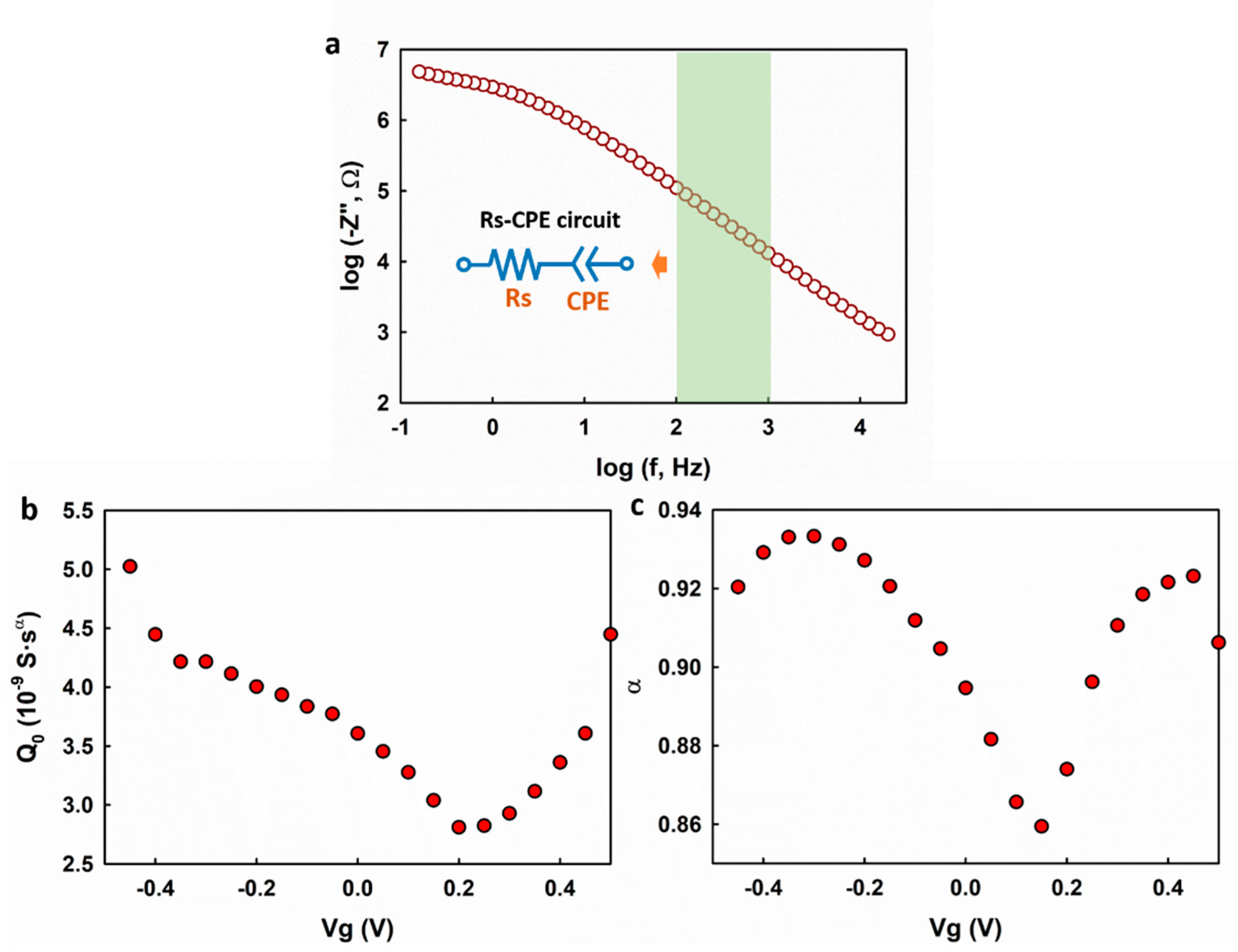
We first studied the frequency response of the graphene electrode using EIS.
Figure 2 shows the representative Bode plot of the graphene electrode. A capacitive regime with a phase shift of ~−80° is observed at 100–1000 Hz. At frequencies lower than 100 Hz, the electrode exhibits a mixed capacitive and resistive response. An equivalent Randles circuit model (inset of
Figure 2b) is used to fit the measured impedance, in which Rs represents the series resistance, including the access resistance and electrolyte resistance, CPE is the constant phase element, Z
f is the faradaic impedance, and Z
w is the Warburg impedance, which is attributed to the diffusion-limited faradaic reaction. The fitting yields a CPE with
= 3.8 × 10
−9 S·s
α and α = 0.89 which corresponds to the capacitive regime with a phase shift of ~−80° in the frequency range of 100–1000 Hz. The results suggest that the electrolyte–-graphene interface behaves as a CPE rather than an ideal capacitor.
Using the Randles circuit model, the impedance spectrum of the graphene electrode was analyzed at different gate voltages. To be consistent with the measured results in the transistor mode, in
Figure 2c,d, the fitting parameters
and α are plotted with respect to
, which equals the negative of the voltages applied to the working electrode.
is normalized with respect to the surface area of the graphene.
exhibits an ambipolar behavior with a minimum of 3.0 × 10
−9 S·s
α at
+0.2 V and increases on both sides of the minimum value. Noting that
is numerically equal to the capacitance at
= 1 Hz, the result is expected and consistent with previous reports [
7,
8,
10]. The non-zero minimum is attributed to the imperfections in graphene, such as the charged impurities on the SiO
2 substrate and the defects in the graphene lattice, which could introduce residual carriers [
8,
10,
18]. However, it is interesting that the factor α also exhibits a dependence on the gate voltage, which is unique for typical EDL.
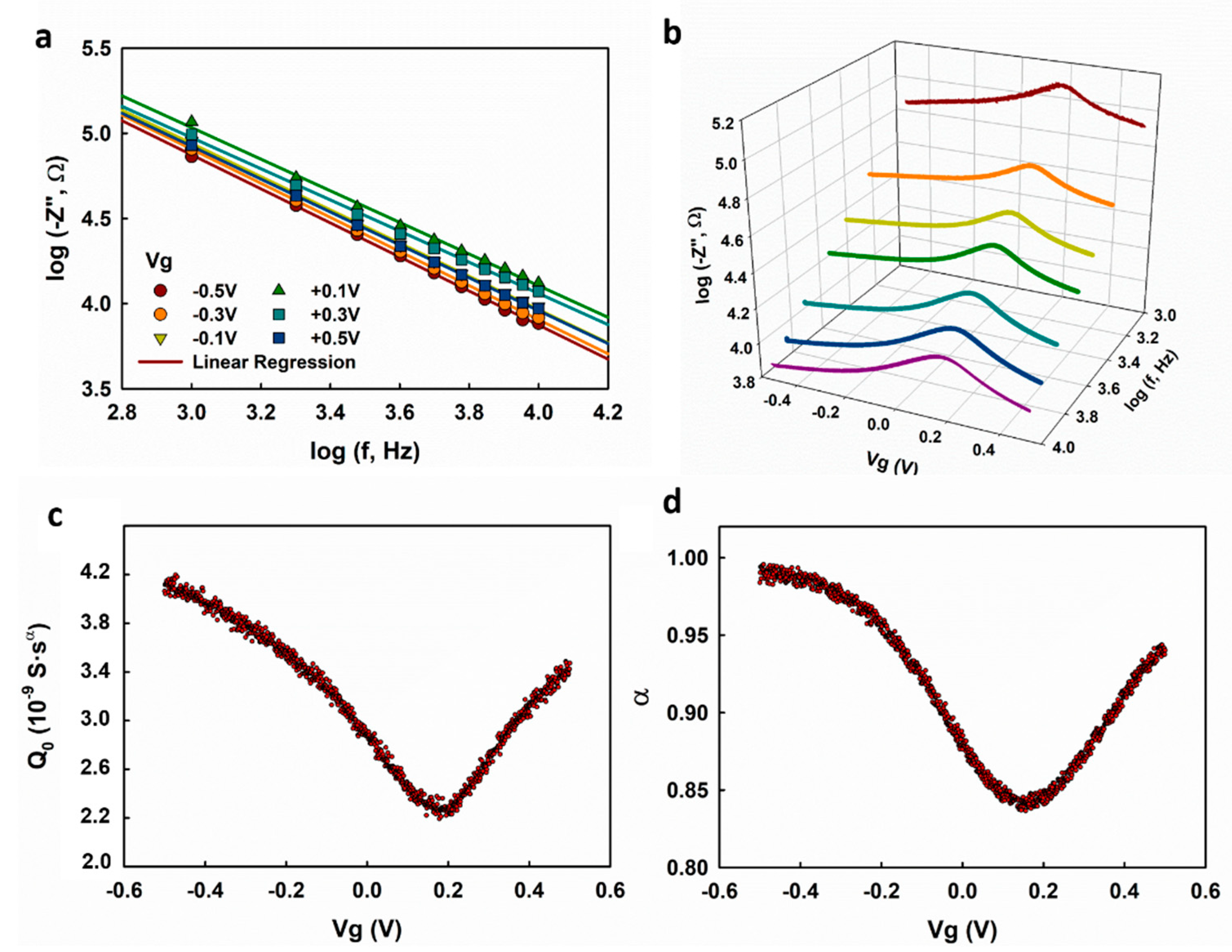
The Randles circuit model was shown to be well fitting to the impedance spectrum. However, it might also introduce uncertainties to the fitting result because a quite few fitting parameters were involved, and this could possibly lead to the observed
-dependence of α. To rule out this possibility, we analyzed the measured impedance spectrum using a simplified electrical circuit model which consists of a resistor and a CPE in a series arrangement as shown in the inset of
Figure 3a. For convenience, the simplified model is called the Rs-CPE model. The Rs-CPE model is based on the analysis of the out of phase elements (
) of the impedance spectrum in the capacitive regime. In the absence of charge transfer induced by the Faradaic reactions at the electrolyte–graphene interface, Z
f and Z
w can be removed leading to a simplified Rs-CPE circuit with the impedance calculated as
The out-of-phase (
) component is
Taking the logarithm of both sides, we get
As shown in
Figure 3a,
. exhibits a good linearity with respect to
, and this is in agreement with Equation (4). A linear regression analysis was applied in the frequency range of 100–1000 Hz to the impedance spectrum collected at different gate potentials. As shown in
Figure 3b,c, both
and
exhibit dependence on the gate voltage (
), which is in accordance with the fitting results using the Randles circuit model. The fitting results from the two different models suggest that the observed gate voltage dependence of
is an intrinsic property of the electrolyte–graphene interface.
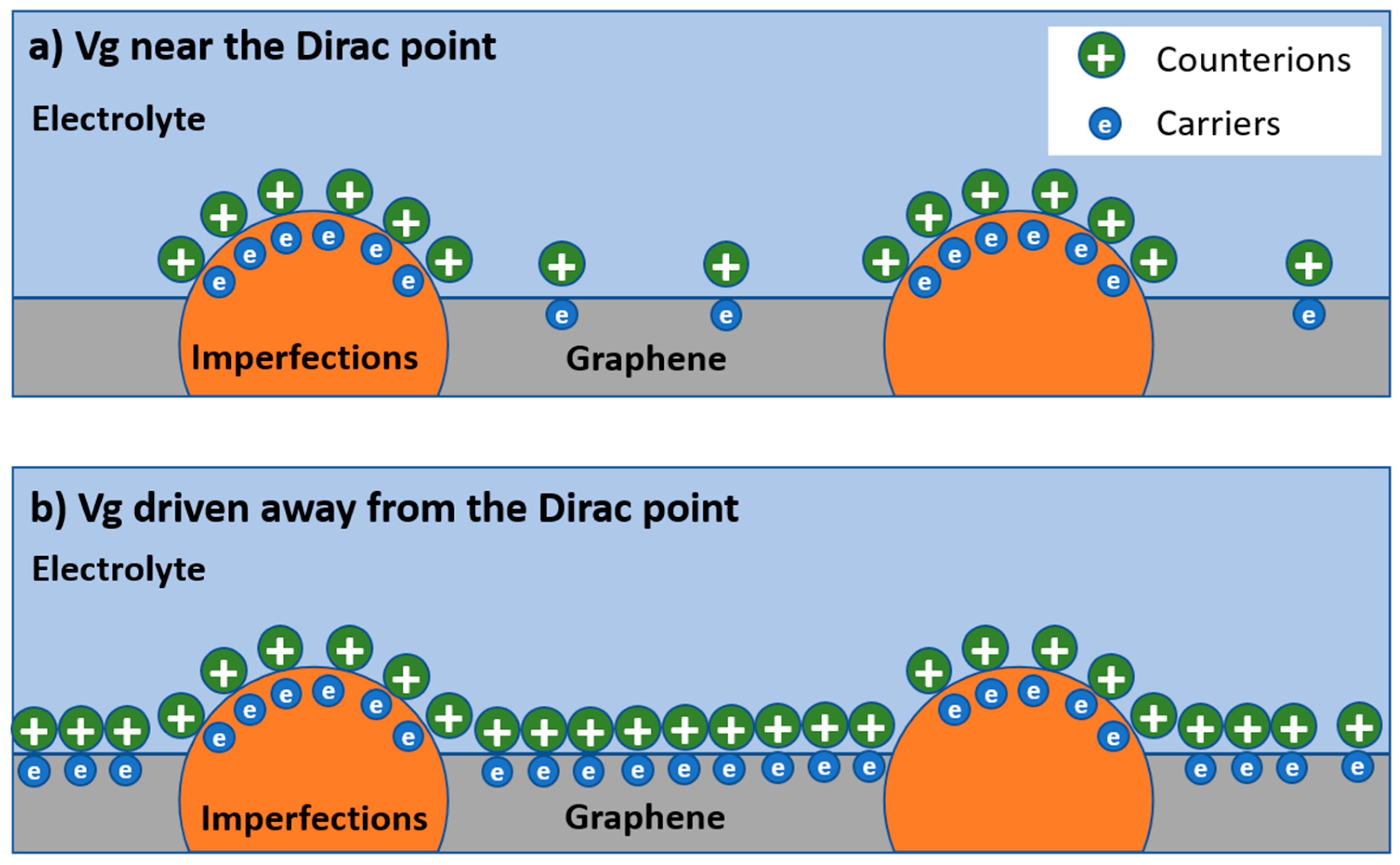
We speculate this unique phenomenon could result from the low DOS in graphene near the Dirac point, which makes
sensitive to the charged impurities on the SiO
2 substrate and the defects in the graphene lattice. The charged impurities on the SiO
2 substrate have a significant impact on the transport behavior of the graphene, such as introducing long-range Coulomb scattering, causing local potential fluctuation and electron/hole puddles [
8,
18], etc. Such effects are well explained by the self-consistent theory [
18]. The presence of defects is evidenced by the D peak in the Raman spectrum of the graphene we used in this study (see
Supplementary Materials, Note 1). These imperfections exist as local sites with DOS that are different from those in the “good” graphene sites. Considering the single-atom-layer structure and low DOS of graphene at a low energy level, these imperfections could dominate the capacitive behavior of the graphene. A schematic diagram depicting this effect is shown in
Figure 4. When the gate potential is low, e.g., near the Dirac point, the carrier density in the graphene is low, and these imperfections dominate the capacitance, resulting in a highly inhomogeneous interface that would give rise to small
values. When the gate potential in graphene is driven away from the Dirac point, the carrier density in graphene is high, and the imperfections are “submerged” by the carriers induced by the gating effect; as a result, the impact of these imperfections is reduced, and a higher
is observed.
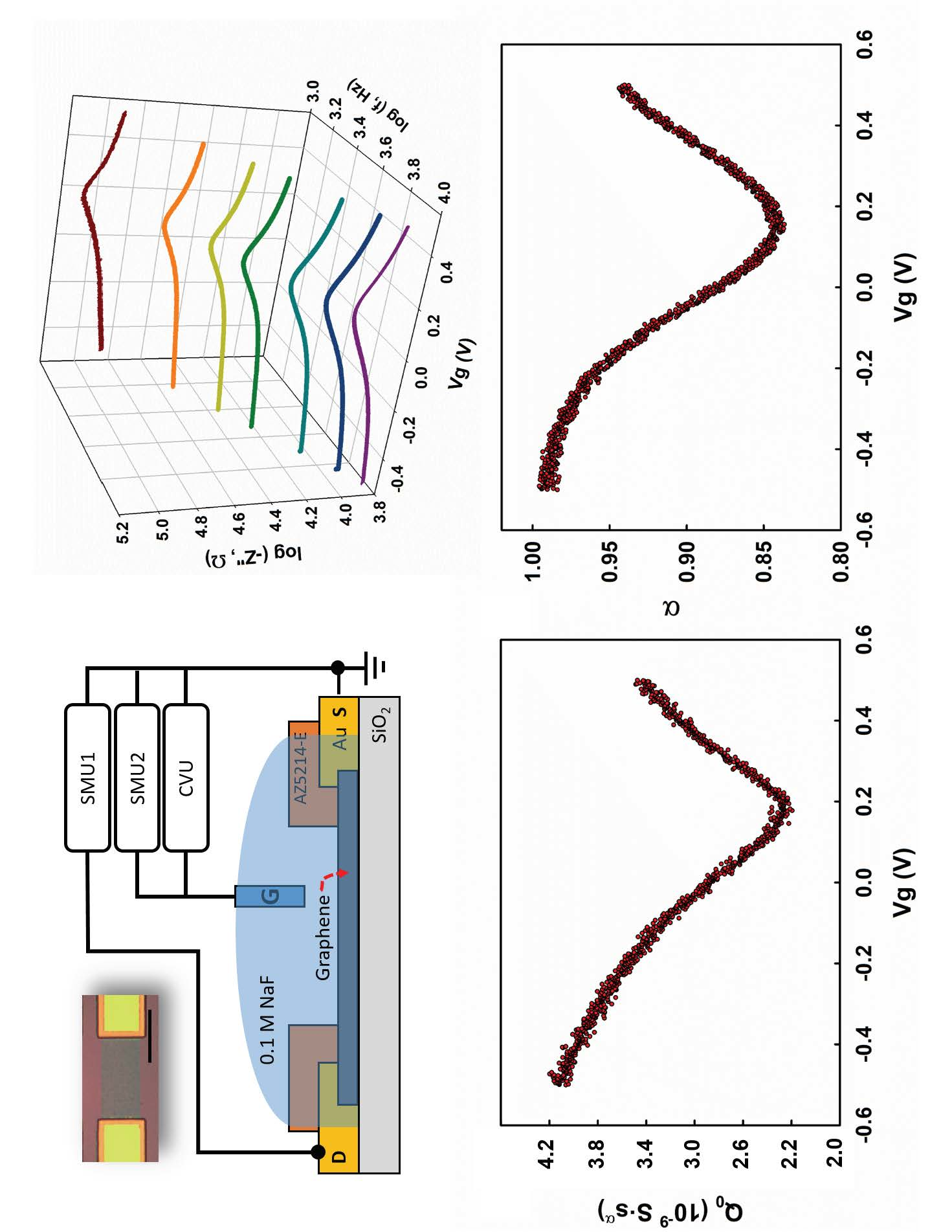
C-V profiling is widely used in the characterization of solid capacitors or transistors [
19]. We demonstrate here the characterization of the electrolyte–graphene interfacial capacitance using a multi-frequency C-V profiling technique and show that it can provide more reliable measurement results than EIS. We first measured the frequency response of the graphene transistor at fixed gate voltages, and the obtained
is plotted with respect to
in
Figure 5a. Good linearity with slopes less than one is observed, suggesting that the graphene transistor works in capacitive regime at 1 k–10 kHz. The impedance of the graphene was then measured at selected frequencies (1, 2, 3, 4, 6, 8, and 10 kHz), and the obtained
is plotted as a function of
in
Figure 5b.
and
are extracted based on the linear regression analysis of
with respect to
using Equation (4), as shown in
Figure 5c,d. Both
and
show dependence on
, which is consistent with the measurement results obtained with EIS, as we discussed previously. Different from the
-
dependence obtained with EIS, which shows decreases at
< −0.3 V and
> +0.4 V (
Figure 2d and
Figure 3c), the
obtained using multi-frequency C-V profiling exhibits a monotonous increase on both sides of the minimum value. We speculate that the latter result is more accurate because (1) the voltage-sweeping mode gives better continuity for the voltage-dependence measurement, and (2) the C-V profiling measurement takes a much shorter time than EIS, which could effectively circumvent the drift of the electrochemical systems.
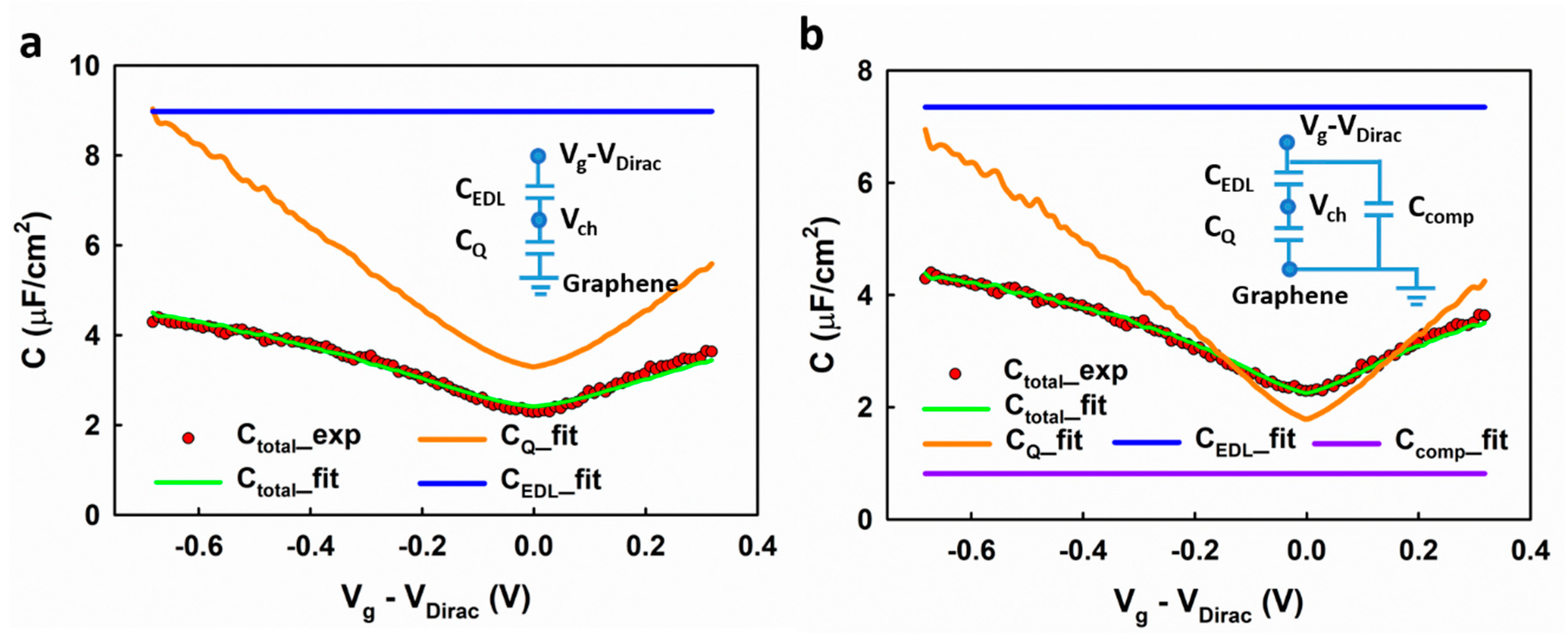
Next, we show the extraction of the carrier density in graphene based on the measured interfacial capacitance, which allows us to calculate the carrier mobility in graphene. Based on the linear DOS in graphene, Fang et al. [
20] derived the quantum capacitance of graphene as a function of the local electrostatic potential (
) as follows (see
Supplementary Materials, Note 2):
in which
is the elementary charge;
is the reduced Planck’s constant;
~ 10
8 cm/s is the Fermi velocity of carriers in graphene. Based on the approximation that the total carrier density in graphene is
in which
is the gate voltage induced carrier density;
is the residue carrier density introduced by the charged impurities. Xia et al. [
8] developed a model for the quantum capacitance
of graphene (see
Supplementary Materials, Note 2 for the derivation of the model):
Considering the series arrangement of the EDL capacitance (
) and the quantum capacitance (
), the total interfacial capacitance (
) can be calculated as
,
, and
can be determined self-consistently by fitting the measured capacitance (
) using Equations (5), (7) and (8). The experimental result can be fitted using this model, as shown in
Figure 6a. However, there is some systematic deviation between the fitted result and the experimental data. For example, at the low voltage range, the fitting results in a slight overestimation of the interfacial capacitance. It is worth noting that a similar deviation is also observed in Xia et al.’s report [
8]. We speculate that such deviation could result from the imperfections in graphene, which present a different DOS profile and therefore behave like an extra capacitor in parallel with the graphene sites. As shown in
Figure 6b, the experimental results can be better fitted by adding a compensating capacitance (
) to the model (inset of
Figure 6b). The fitting gives a residual carrier density
= 1.36 × 10
12 cm
−2, which is comparable to previous reports [
18,
21]. Comparing with the previous report [
8], in which the
was determined by theoretical prediction, our self-consistent fitting method could provide a more accurate result.
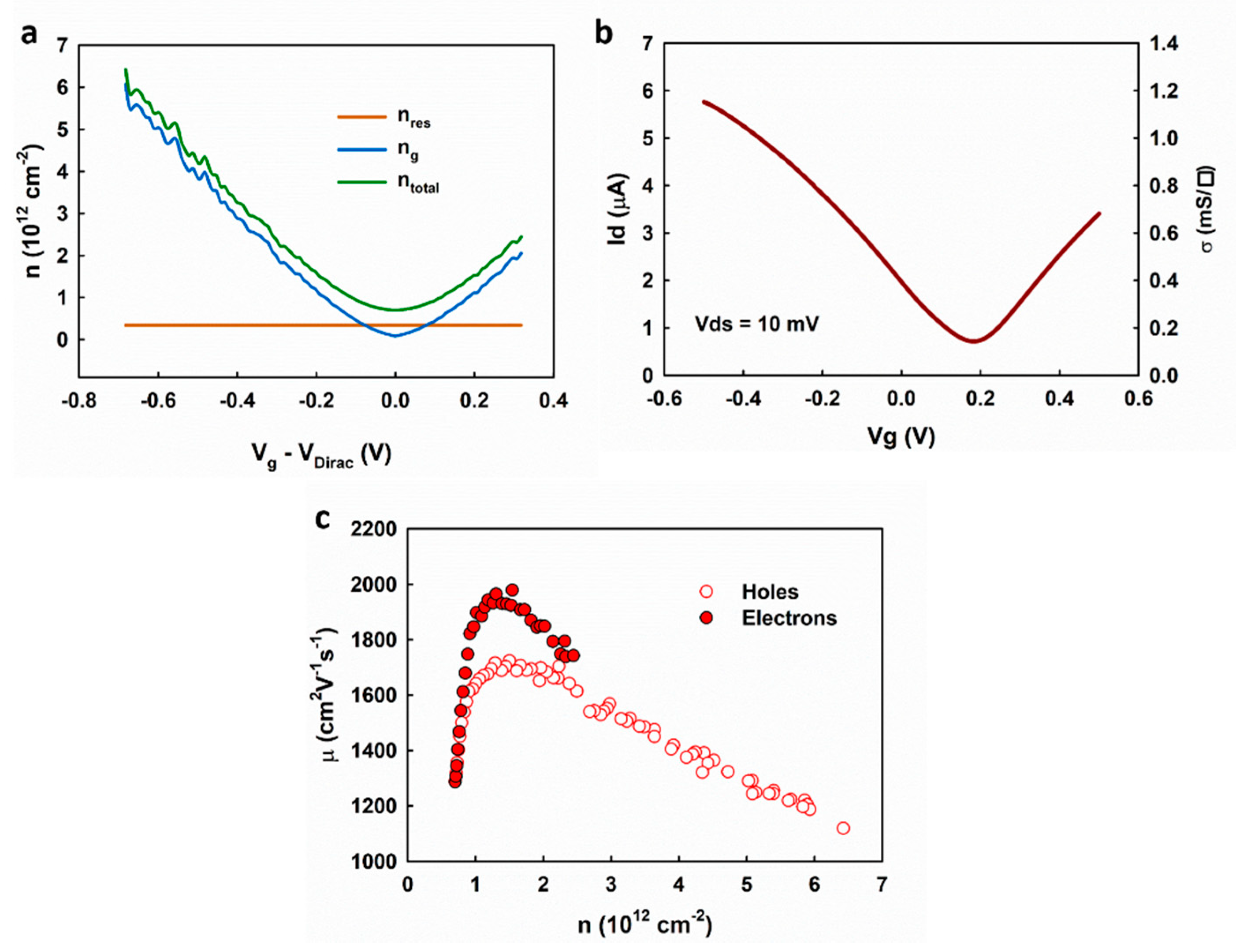
The carrier mobility can be extracted based on the Drude model:
in which
is the sheet conductivity of graphene;
and
are the density of electrons and holes, respectively;
and
are the mobility of electrons and holes, respectively. The carrier densities
and
were extracted based on the fitting results of the measured capacitance (
Figure 6b). Based on the mass-action law, we applied a correction to the overall carrier density as
in which
is the residue carrier density
. As shown in
Figure 7a, the total carrier density can be calculated as
The sheet conductivity of graphene was calculated based on the transfer measurement of the electrolyte-gated graphene transistor after evaluating the access resistance shown in
Figure 7b and
Supplementary Materials, Note 3. The extracted carrier mobilities are plotted in
Figure 7c, showing a similar dependence on the carrier density as the results given in Reference [
22]. The highest mobilities are ~1700 and ~2000 cm
2V
−1s
−1, for holes and electrons, respectively, and decreases when the carrier density is higher than ~1.5 × 10
12 cm
−2. The results suggest the transition of the scattering mechanism from the long-range Coulomb scattering (i.e., charged impurities) near the Dirac point to the short-range scattering, which is in agreement with the self-consistent theory [
18]. Our results are different from those obtained by the Hall effect measurement [
23,
24], which shows the highest mobility at the Dirac point and monotonous decrease as the carrier density increases. This is because the Hall effect cannot measure the density of the residual carrier (the Hall voltages induced by the electrons and the holes cancel each other) and thus cause the overestimation of the carrier mobilities near the Dirac point.


