GFET Asymmetric Transfer Response Analysis through Access Region Resistances

 ,
,  ,
,  , , , and
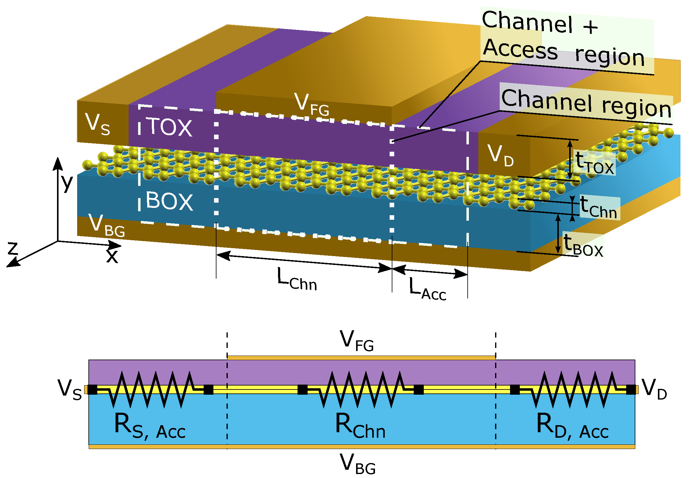
Abstract
1. Introduction
2. Results
2.1. Device Simulation
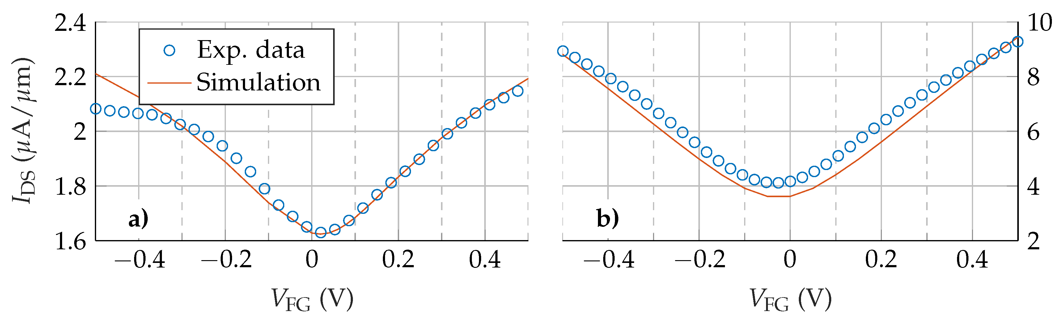
2.2. Validation
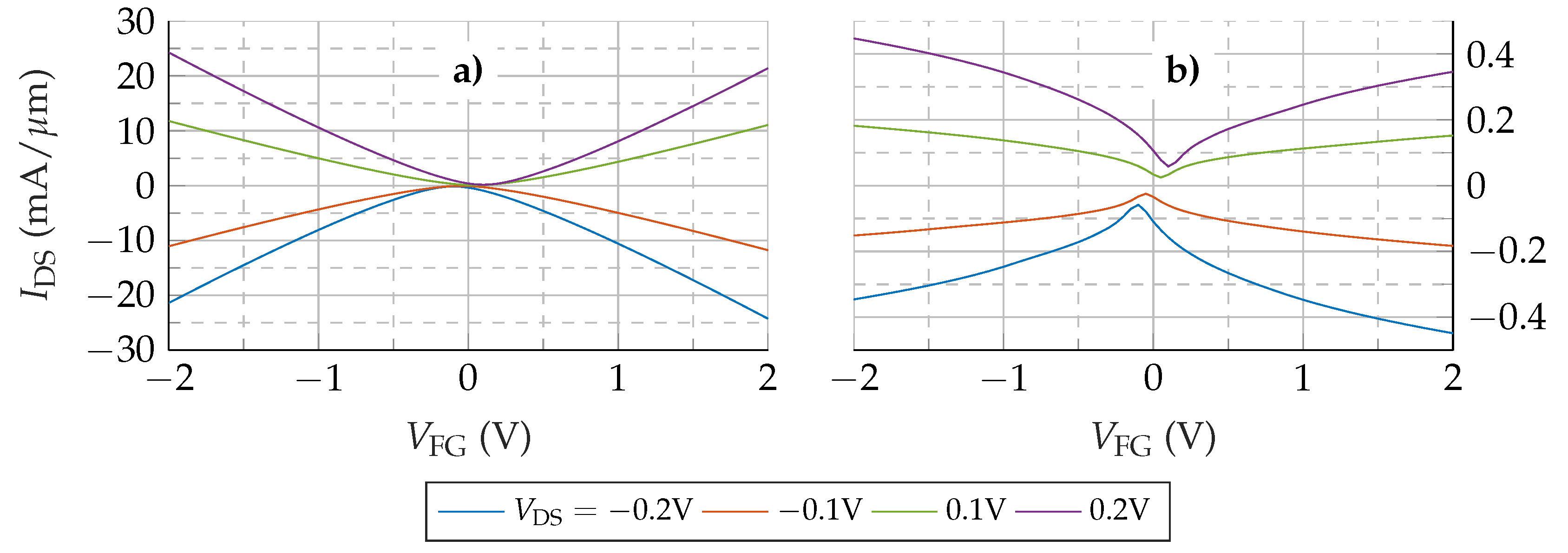
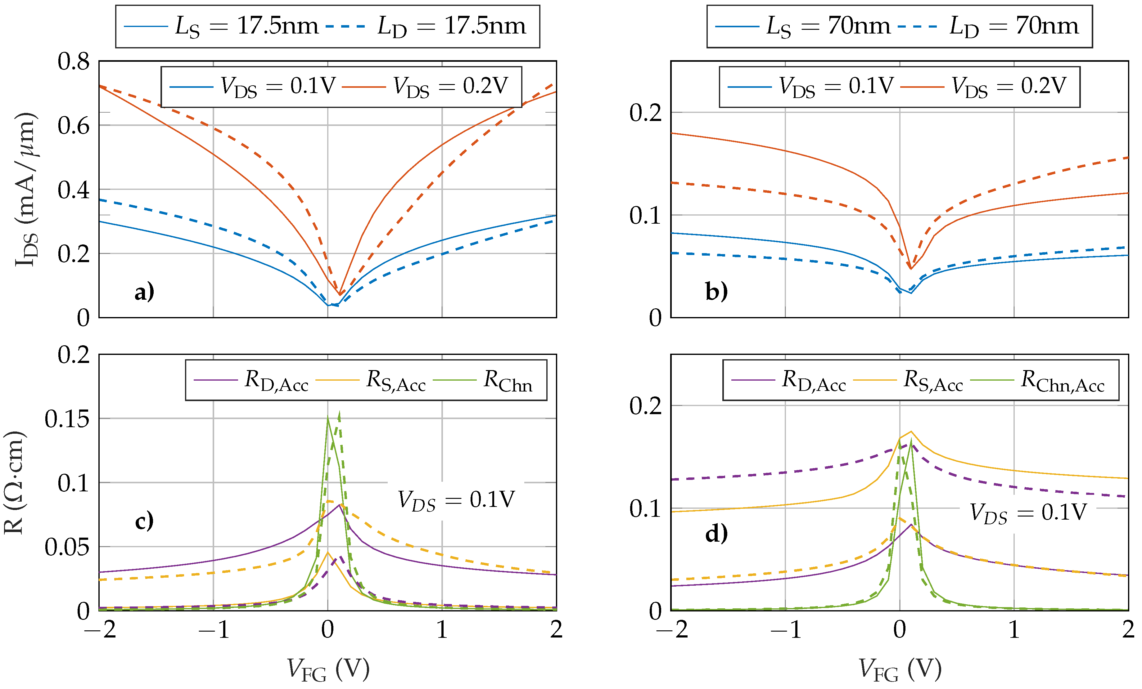
2.3. Access Region Analysis
2.3.1. Including the Access Regions
2.3.2. Gate Misalignment
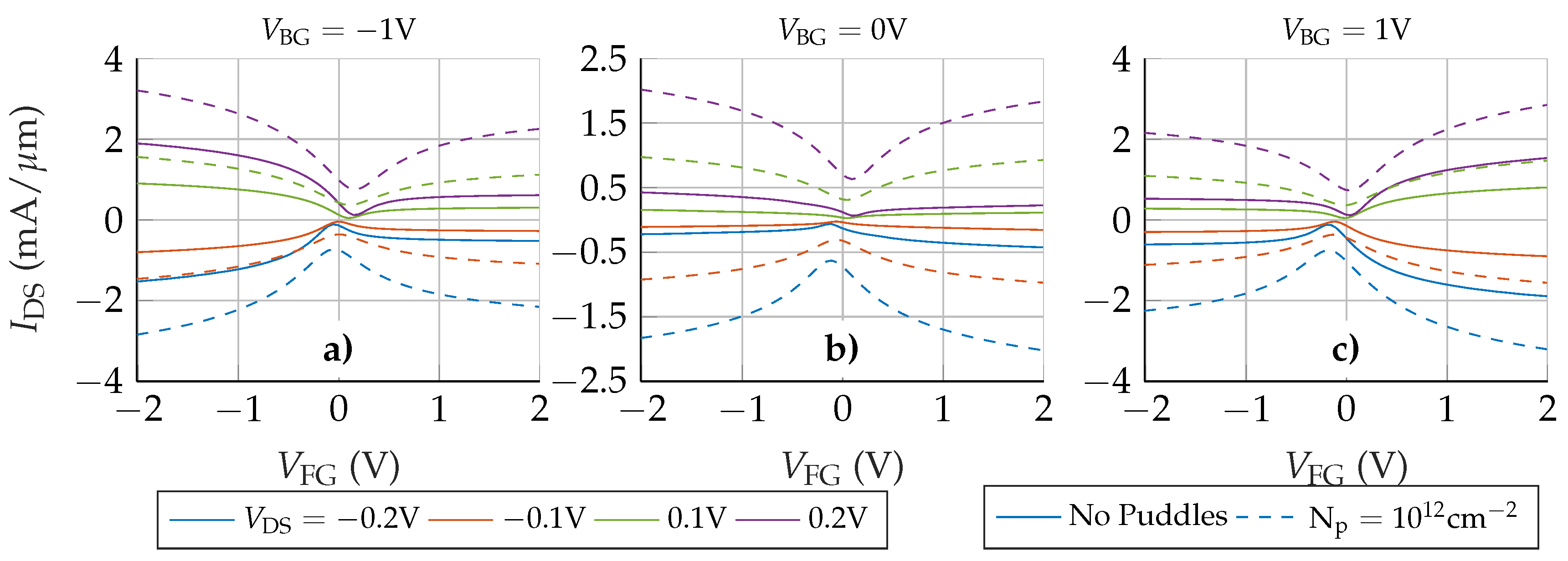
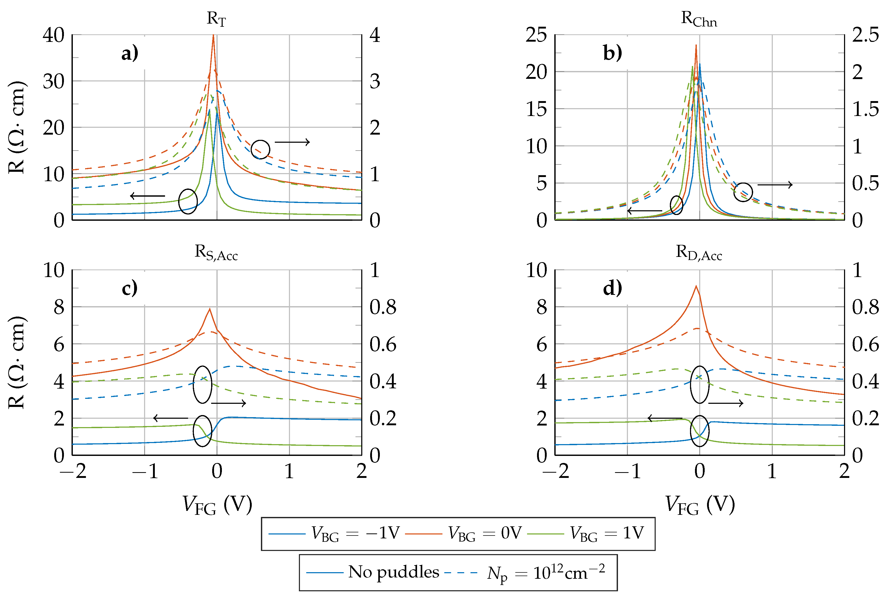
2.3.3. Impact of Electrostatic Doping and Puddles
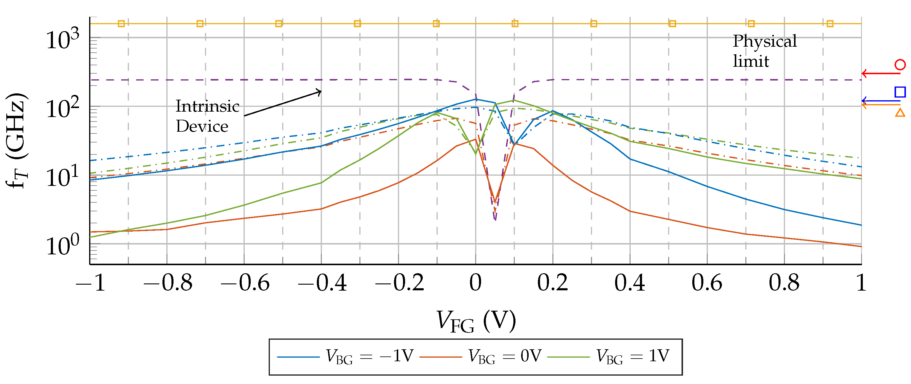
2.3.4. RF Performance
3. Conclusions
Author Contributions
Funding
Conflicts of Interest
Abbreviations
| 2DM | Two-dimensional material |
| MOSFET | Metal-Oxide-Semiconductor Field-Effect Transistor |
| GFET | Graphene Field-Effect Transistors |
| RF | Radio-Frequency |
References
- Fiori, G.; Bonaccorso, F.; Iannaccone, G.; Palacios, T.; Neumaier, D.; Seabaugh, A.; Banerjee, S.K.; Colombo, L. Electronics based on two-dimensional materials. Nat. Nanotechnol. 2014, 9, 768–779. [Google Scholar] [CrossRef] [PubMed]
- Lee, S.; Zhong, Z. Nanoelectronic circuits based on two-dimensional atomic layer crystals. Nanoscale 2014, 6, 13283–13300. [Google Scholar] [CrossRef] [PubMed]
- Neto, A.H.C.; Guinea, F.; Peres, N.M.R.; Novoselov, K.S.; Geim, A.K. The electronic properties of graphene. Rev. Mod. Phys. 2009, 81, 109–162. [Google Scholar] [CrossRef]
- Guerriero, E.; Pedrinazzi, P.; Mansouri, A.; Habibpour, O.; Winters, M.; Rorsman, N.; Behnam, A.; Carrion, E.A.; Pesquera, A.; Centeno, A.; et al. High-Gain Graphene Transistors with a Thin AlOx Top-Gate Oxide. Sci. Rep. 2017, 7, 2419. [Google Scholar] [CrossRef] [PubMed]
- Lin, Y.M.; Jenkins, K.A.; Valdes-Garcia, A.; Small, J.P.; Farmer, D.B.; Avouris, P. Operation of Graphene Transistors at Gigahertz Frequencies. Nano Lett. 2009, 9, 422–426. [Google Scholar] [CrossRef]
- Meric, I.; Han, M.Y.; Young, A.F.; Ozyilmaz, B.; Kim, P.; Shepard, K.L. Current saturation in zero-bandgap, top-gated graphene field-effect transistors. Nat. Nanotechnol. 2008, 3, 654–659. [Google Scholar] [CrossRef] [PubMed]
- Rizzi, L.G.; Bianchi, M.; Behnam, A.; Carrion, E.; Guerriero, E.; Polloni, L.; Pop, E.; Sordan, R. Cascading Wafer-Scale Integrated Graphene Complementary Inverters under Ambient Conditions. Nano Lett. 2012, 12, 3948–3953. [Google Scholar] [CrossRef] [PubMed]
- Pandey, H.; Shaygan, M.; Sawallich, S.; Kataria, S.; Wang, Z.; Noculak, A.; Otto, M.; Nagel, M.; Negra, R.; Neumaier, D.; et al. All CVD Boron Nitride Encapsulated Graphene FETs With CMOS Compatible Metal Edge Contacts. IEEE Trans. Electron Devices 2018, 65, 4129–4134. [Google Scholar] [CrossRef]
- Wu, Y.; Zou, X.; Sun, M.; Cao, Z.; Wang, X.; Huo, S.; Zhou, J.; Yang, Y.; Yu, X.; Kong, Y.; et al. 200 GHz Maximum Oscillation Frequency in CVD Graphene Radio Frequency Transistors. ACS Appl. Mater. Interfaces 2016, 8, 25645–25649. [Google Scholar] [CrossRef]
- Cheng, R.; Bai, J.; Liao, L.; Zhou, H.; Chen, Y.; Liu, L.; Lin, Y.C.; Jiang, S.; Huang, Y.; Duan, X. High-frequency self-aligned graphene transistors with transferred gate stacks. Proc. Natl. Acad. Sci. USA 2012, 109, 11588–11592. [Google Scholar] [CrossRef]
- Lin, Y.M.; Dimitrakopoulos, C.; Jenkins, K.A.; Farmer, D.B.; Chiu, H.Y.; Grill, A.; Avouris, P. 100-GHz Transistors from Wafer-Scale Epitaxial Graphene. Science 2010, 327, 662. [Google Scholar] [CrossRef] [PubMed]
- Georgiou, T.; Jalil, R.; Belle, B.D.; Britnell, L.; Gorbachev, R.V.; Morozov, S.V.; Kim, Y.J.; Gholinia, A.; Haigh, S.J.; Makarovsky, O.; et al. Vertical field-effect transistor based on graphene–WS2 heterostructures for flexible and transparent electronics. Nat. Nanotechnol. 2013, 8, 100–103. [Google Scholar] [CrossRef] [PubMed]
- Wang, Z.; Uzlu, B.; Shaygan, M.; Otto, M.; Ribeiro, M.; Marín, E.G.; Iannaccone, G.; Fiori, G.; Elsayed, M.S.; Negra, R.; et al. Flexible One-Dimensional Metal–Insulator–Graphene Diode. ACS Appl. Electron. Mater. 2019, 1, 945–950. [Google Scholar] [CrossRef]
- Liao, L.; Bai, J.; Cheng, R.; Lin, Y.C.; Jiang, S.; Huang, Y.; Duan, X. Top-Gated Graphene Nanoribbon Transistors with Ultrathin High-kDielectrics. Nano Lett. 2010, 10, 1917–1921. [Google Scholar] [CrossRef] [PubMed]
- Mayorov, A.S.; Gorbachev, R.V.; Morozov, S.V.; Britnell, L.; Jalil, R.; Ponomarenko, L.A.; Blake, P.; Novoselov, K.S.; Watanabe, K.; Taniguchi, T.; et al. Micrometer-Scale Ballistic Transport in Encapsulated Graphene at Room Temperature. Nano Lett. 2011, 11, 2396–2399. [Google Scholar] [CrossRef] [PubMed]
- Farmer, D.B.; Lin, Y.M.; Avouris, P. Graphene field-effect transistors with self-aligned gates. Appl. Phys. Lett. 2010, 97, 013103. [Google Scholar] [CrossRef]
- Feng, Z.; Yu, C.; Li, J.; Liu, Q.; He, Z.; Song, X.; Wang, J.; Cai, S. An ultra clean self-aligned process for high maximum oscillation frequency graphene transistors. Carbon 2014, 75, 249–254. [Google Scholar] [CrossRef]
- Fiori, G.; Iannaccone, G. Multiscale Modeling for Graphene-Based Nanoscale Transistors. Proc. IEEE 2013, 101, 1653–1669. [Google Scholar] [CrossRef]
- Di Bartolomeo, A.; Giubileo, F.; Romeo, F.; Sabatino, P.; Carapella, G.; Iemmo, L.; Schroeder, T.; Lupina, G. Graphene field effect transistors with niobium contacts and asymmetric transfer characteristics. Nanotechnology 2015, 26, 475202. [Google Scholar] [CrossRef]
- Jain, S.; Dutta, A.K. Resistance-Based Approach for Drain Current Modeling in Graphene FETs. IEEE Trans. Electron Devices 2015, 62, 4313–4321. [Google Scholar] [CrossRef]
- Al-Amin, C.; Karabiyik, M.; Pala, N. Fabrication of Graphene Field-effect Transistor with Field Controlling Electrodes to improve fT. Microelectron. Eng. 2016, 164, 71–74. [Google Scholar] [CrossRef]
- Wang, H.; Hsu, A.; Kong, J.; Antoniadis, D.A.; Palacios, T. Compact Virtual-Source Current–Voltage Model for Top- and Back-Gated Graphene Field-Effect Transistors. IEEE Trans. Electron Devices 2011, 58, 1523–1533. [Google Scholar] [CrossRef]
- Ancona, M.G. Electron Transport in Graphene From a Diffusion-Drift Perspective. IEEE Trans. Electron Devices 2010, 57, 681–689. [Google Scholar] [CrossRef]
- Curatola, G.; Doornbos, G.; Loo, J.; Ponomarev, Y.; Iannaccone, G. Detailed Modeling of Sub-100-nm MOSFETs Based on Schrödinger DD Per Subband and Experiments and Evaluation of the Performance Gap to Ballistic Transport. IEEE Trans. Electron Devices 2005, 52, 1851–1858. [Google Scholar] [CrossRef]
- Feijoo, P.C.; Jiménez, D.; Cartoixà, X. Short channel effects in graphene-based field effect transistors targeting radio-frequency applications. 2D Mater. 2016, 3, 025036. [Google Scholar] [CrossRef]
- Wilmart, Q.; Inhofer, A.; Boukhicha, M.; Yang, W.; Rosticher, M.; Morfin, P.; Garroum, N.; Fève, G.; Berroir, J.M.; Plaçais, B. Contact gating at GHz frequency in graphene. Sci. Rep. 2016, 6, 21085. [Google Scholar] [CrossRef]
- Martin, J.; Akerman, N.; Ulbricht, G.; Lohmann, T.; Smet, J.H.; von Klitzing, K.; Yacoby, A. Observation of electron–hole puddles in graphene using a scanning single-electron transistor. Nat. Phys. 2007, 4, 144–148. [Google Scholar] [CrossRef]
- Fregonese, S.; Magallo, M.; Maneux, C.; Happy, H.; Zimmer, T. Scalable Electrical Compact Modeling for Graphene FET Transistors. IEEE Trans. Nanotechnol. 2013, 12, 539–546. [Google Scholar] [CrossRef]
- Wang, Z.; Xu, H.; Zhang, Z.; Wang, S.; Ding, L.; Zeng, Q.; Yang, L.; Pei, T.; Liang, X.; Gao, M.; et al. Growth and Performance of Yttrium Oxide as an Ideal High-k Gate Dielectric for Carbon-Based Electronics. Nano Lett. 2010, 10, 2024–2030. [Google Scholar] [CrossRef]
- Zhang, Z.; Xu, H.; Zhong, H.; Peng, L.M. Direct extraction of carrier mobility in graphene field-effect transistor using current-voltage and capacitance-voltage measurements. Appl. Phys. Lett. 2012, 101, 213103. [Google Scholar] [CrossRef]
- Venica, S.; Zanato, M.; Driussi, F.; Palestri, P.; Selmi, L. Modeling electrostatic doping and series resistance in graphene-FETs. In Proceedings of the 2016 International Conference on Simulation of Semiconductor Processes and Devices (SISPAD), Nuremberg, Germany, 6–8 September 2016. [Google Scholar] [CrossRef]
- Zhang, Y.; Brar, V.W.; Girit, C.; Zettl, A.; Crommie, M.F. Origin of spatial charge inhomogeneity in graphene. Nat. Phys. 2009, 5, 722–726. [Google Scholar] [CrossRef]
- Marian, D.; Dib, E.; Cusati, T.; Marin, E.G.; Fortunelli, A.; Iannaccone, G.; Fiori, G. Transistor Concepts Based on Lateral Heterostructures of Metallic and Semiconducting Phases of MoS2. Phys. Rev. Appl. 2017, 8, 054047. [Google Scholar] [CrossRef]
- Schwierz, F. Graphene Transistors: Status, Prospects, and Problems. Proc. IEEE 2013, 101, 1567–1584. [Google Scholar] [CrossRef]
- Liao, L.; Lin, Y.C.; Bao, M.; Cheng, R.; Bai, J.; Liu, Y.; Qu, Y.; Wang, K.L.; Huang, Y.; Duan, X. High-speed graphene transistors with a self-aligned nanowire gate. Nature 2010, 467, 305–308. [Google Scholar] [CrossRef]
- Wu, Y.; Jenkins, K.A.; Valdes-Garcia, A.; Farmer, D.B.; Zhu, Y.; Bol, A.A.; Dimitrakopoulos, C.; Zhu, W.; Xia, F.; Avouris, P.; et al. State-of-the-Art Graphene High-Frequency Electronics. Nano Lett. 2012, 12, 3062–3067. [Google Scholar] [CrossRef]


© 2019 by the authors. Licensee MDPI, Basel, Switzerland. This article is an open access article distributed under the terms and conditions of the Creative Commons Attribution (CC BY) license (http://creativecommons.org/licenses/by/4.0/).
Share and Cite
Toral-Lopez, A.; Marin, E.G.; Pasadas, F.; Gonzalez-Medina, J.M.; Ruiz, F.G.; Jiménez, D.; Godoy, A. GFET Asymmetric Transfer Response Analysis through Access Region Resistances. Nanomaterials 2019, 9, 1027. https://doi.org/10.3390/nano9071027
Toral-Lopez A, Marin EG, Pasadas F, Gonzalez-Medina JM, Ruiz FG, Jiménez D, Godoy A. GFET Asymmetric Transfer Response Analysis through Access Region Resistances. Nanomaterials. 2019; 9(7):1027. https://doi.org/10.3390/nano9071027
Chicago/Turabian StyleToral-Lopez, Alejandro, Enrique G. Marin, Francisco Pasadas, Jose Maria Gonzalez-Medina, Francisco G. Ruiz, David Jiménez, and Andres Godoy. 2019. "GFET Asymmetric Transfer Response Analysis through Access Region Resistances" Nanomaterials 9, no. 7: 1027. https://doi.org/10.3390/nano9071027
APA StyleToral-Lopez, A., Marin, E. G., Pasadas, F., Gonzalez-Medina, J. M., Ruiz, F. G., Jiménez, D., & Godoy, A. (2019). GFET Asymmetric Transfer Response Analysis through Access Region Resistances. Nanomaterials, 9(7), 1027. https://doi.org/10.3390/nano9071027