Graphene Schottky Junction on Pillar Patterned Silicon Substrate

 ,
,  , and
, and 
Abstract
1. Introduction
2. Materials and Methods
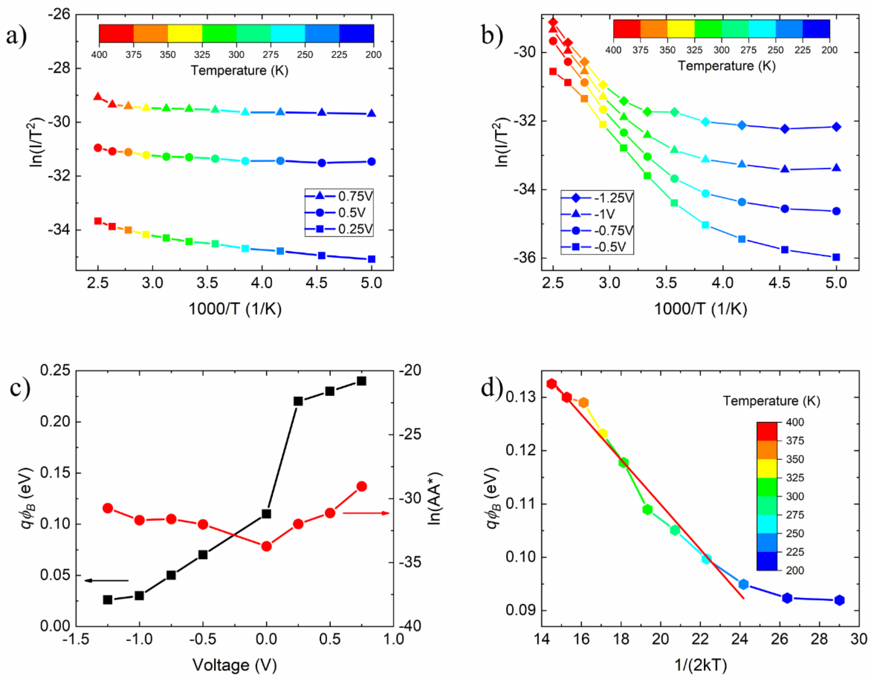
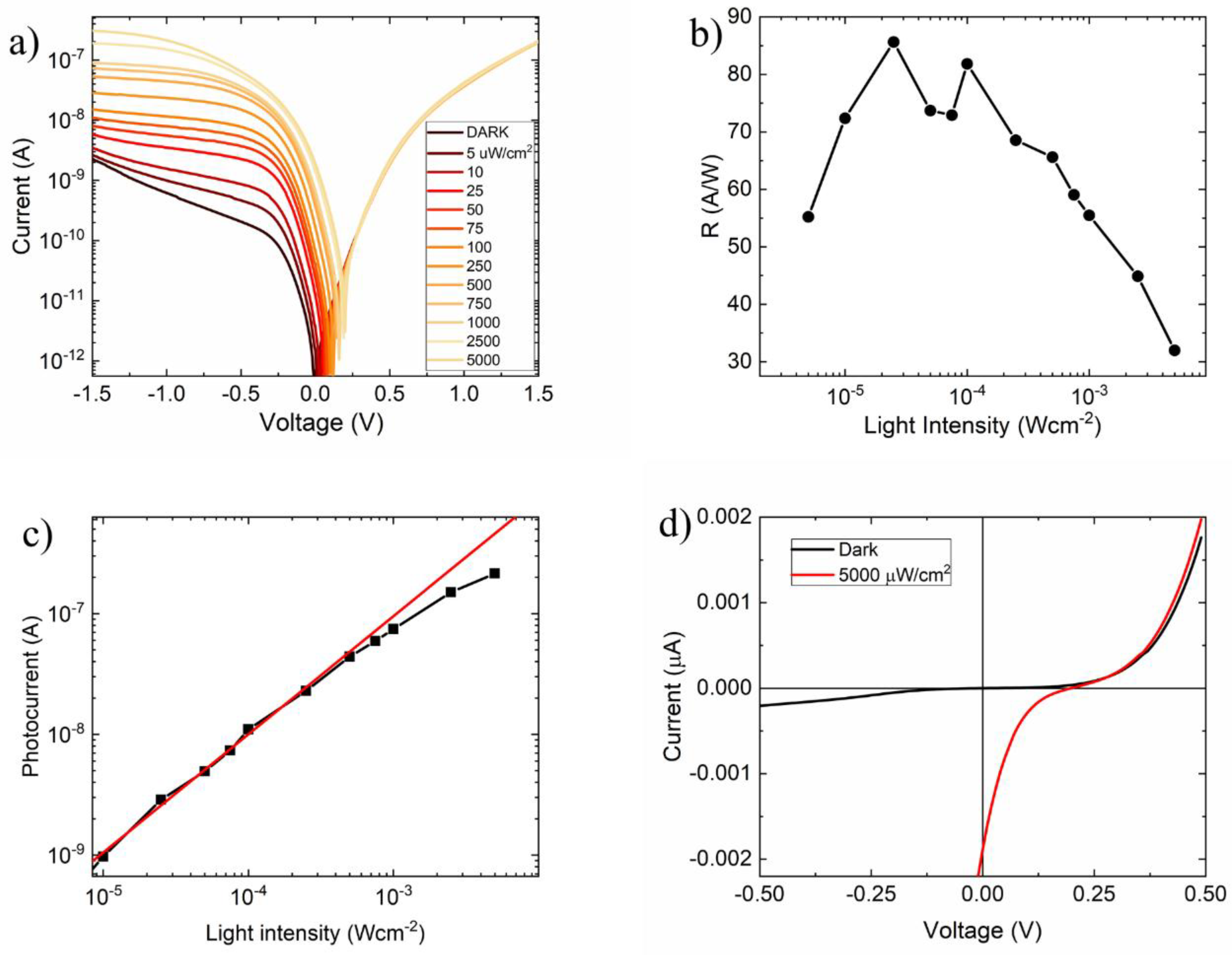
3. Results
4. Conclusions
Author Contributions
Funding
Acknowledgments
Conflicts of Interest
References
- Geim, A.K.; Novoselov, K.S. The rise of graphene. Nat. Mater. 2007, 6, 183–191. [Google Scholar] [CrossRef] [PubMed]
- Ganatra, R.; Zhang, Q. Few-Layer MoS2: A promising layered semiconductor. ACS Nano 2014, 8, 4074–4099. [Google Scholar] [CrossRef]
- Di Bartolomeo, A.; Genovese, L.; Giubileo, F.; Iemmo, L.; Luongo, G.; Foller, T.; Schleberger, M. Hysteresis in the transfer characteristics of MoS2 transistors. 2D Mater. 2017, 5, 015014. [Google Scholar] [CrossRef]
- Li, H.; Lu, G.; Wang, Y.; Yin, Z.; Cong, C.; He, Q.; Wang, L.; Ding, F.; Yu, T.; Zhang, H. Mechanical exfoliation and characterization of single- and few-layer nanosheets of WSe2, TaS2, and TaSe2. Small 2013, 9, 1974–1981. [Google Scholar] [CrossRef]
- Di Bartolomeo, A.; Urban, F.; Passacantando, M.; McEvoy, N.; Peters, L.; Iemmo, L.; Luongo, G.; Romeo, F.; Giubileo, F. A WSe 2 vertical field emission transistor. Nanoscale 2019, 11, 1538–1548. [Google Scholar] [CrossRef] [PubMed]
- Carvalho, A.; Wang, M.; Zhu, X.; Rodin, A.S.; Su, H.; Castro Neto, A.H. Phosphorene: From theory to applications. Nat. Rev. Mater. 2016, 1, 16061. [Google Scholar] [CrossRef]
- Castro, N.A.H.; Guinea, F.; Peres, N.M.R.; Novoselov, K.S.; Geim, A.K. The electronic properties of graphene. Rev. Modern Phys. 2009, 81, 109–162. [Google Scholar] [CrossRef]
- Xia, F.; Perebeinos, V.; Lin, Y.; Wu, Y.; Avouris, P. The origins and limits of metal–graphene junction resistance. Nat. Nanotechnol. 2011, 6, 179–184. [Google Scholar] [CrossRef]
- Di Bartolomeo, A.; Santandrea, S.; Giubileo, F.; Romeo, F.; Petrosino, M.; Citro, R.; Barbara, P.; Lupina, G.; Schroeder, T.; Rubino, A. Effect of back-gate on contact resistance and on channel conductance in graphene-based field-effect transistors. Diam. Relat. Mater. 2013, 38, 19–23. [Google Scholar] [CrossRef]
- Bartolomeo, A.D.; Giubileo, F.; Romeo, F.; Sabatino, P.; Carapella, G.; Iemmo, L.; Schroeder, T.; Lupina, G. Graphene field effect transistors with niobium contacts and asymmetric transfer characteristics. Nanotechnology 2015, 26, 475202. [Google Scholar] [CrossRef] [PubMed]
- Giubileo, F.; Di Bartolomeo, A. The role of contact resistance in graphene field-effect devices. Prog. Surf. Sci. 2017, 92, 143–175. [Google Scholar] [CrossRef]
- Di Bartolomeo, A.; Giubileo, F.; Iemmo, L.; Romeo, F.; Russo, S.; Unal, S.; Passacantando, M.; Grossi, V.; Cucolo, A.M. Leakage and field emission in side-gate graphene field effect transistors. Appl. Phys. Lett. 2016, 109, 023510. [Google Scholar] [CrossRef]
- Yang, H.; Heo, J.; Park, S.; Song, H.J.; Seo, D.H.; Byun, K.-E.; Kim, P.; Yoo, I.; Chung, H.-J.; Kim, K. Graphene barristor, a triode device with a gate-controlled schottky barrier. Science 2012, 336, 1140–1143. [Google Scholar] [CrossRef]
- Mehr, W.; Dabrowski, J.; Scheytt, J.C.; Lippert, G.; Xie, Y.-H.; Lemme, M.C.; Ostling, M.; Lupina, G. Vertical graphene base transistor. IEEE Electr. Dev. Lett. 2012, 33, 691–693. [Google Scholar] [CrossRef]
- Chen, C.-C.; Aykol, M.; Chang, C.-C.; Levi, A.F.J.; Cronin, S.B. Graphene-silicon schottky diodes. Nano Lett. 2011, 11, 1863–1867. [Google Scholar] [CrossRef]
- Di Bartolomeo, A.; Luongo, G.; Giubileo, F.; Funicello, N.; Niu, G.; Schroeder, T.; Lisker, M.; Lupina, G. Hybrid graphene/silicon Schottky photodiode with intrinsic gating effect. 2D Mater. 2017, 4, 025075. [Google Scholar] [CrossRef]
- Di Bartolomeo, A.; Giubileo, F.; Luongo, G.; Iemmo, L.; Martucciello, N.; Niu, G.; Fraschke, M.; Skibitzki, O.; Schroeder, T.; Lupina, G. Tunable Schottky barrier and high responsivity in graphene/Si-nanotip optoelectronic device. 2D Mater. 2016, 4, 015024. [Google Scholar] [CrossRef]
- Luongo, G.; Giubileo, F.; Genovese, L.; Iemmo, L.; Martucciello, N.; Di Bartolomeo, A. I-V and C-V characterization of a high-responsivity graphene/silicon photodiode with embedded MOS capacitor. Nanomaterials 2017, 7, 158. [Google Scholar] [CrossRef]
- Luongo, G.; Di Bartolomeo, A.; Giubileo, F.; Chavarin, C.A.; Wenger, C. Electronic properties of graphene/p-silicon Schottky junction. J. Phys. D Appl. Phys. 2018, 51, 255305. [Google Scholar] [CrossRef]
- Luongo, G.; Giubileo, F.; Iemmo, L.; Di Bartolomeo, A. The role of the substrate in Graphene/Silicon photodiodes. J. Physi. Conf. Ser. 2018, 956, 012019. [Google Scholar] [CrossRef]
- Kim, H.-Y.; Lee, K.; McEvoy, N.; Yim, C.; Duesberg, G.S. Chemically modulated graphene diodes. Nano Lett. 2013, 13, 2182–2188. [Google Scholar] [CrossRef]
- Singh, A.; Uddin, M.A.; Sudarshan, T.; Koley, G. Tunable Reverse-biased graphene/silicon heterojunction schottky diode sensor. Small 2014, 10, 1555–1565. [Google Scholar] [CrossRef]
- Fattah, A.; Khatami, S.; Mayorga-Martinez, C.C.; Medina-Sánchez, M.; Baptista-Pires, L.; Merkoçi, A. Graphene/silicon heterojunction schottky diode for vapors sensing using impedance spectroscopy. Small 2014, 10, 4193–4199. [Google Scholar] [CrossRef] [PubMed]
- Riazimehr, S.; Bablich, A.; Schneider, D.; Kataria, S.; Passi, V.; Yim, C.; Duesberg, G.S.; Lemme, M.C. Spectral sensitivity of graphene/silicon heterojunction photodetectors. Solid State Electron. 2016, 115, 207–212. [Google Scholar] [CrossRef]
- Bonaccorso, F.; Sun, Z.; Hasan, T.; Ferrari, A.C. Graphene photonics and optoelectronics. Nat. Photonics 2010, 4, 611–622. [Google Scholar] [CrossRef]
- An, X.; Liu, F.; Jung, Y.J.; Kar, S. Tunable graphene–silicon heterojunctions for ultrasensitive photodetection. Nano Lett. 2013, 13, 909–916. [Google Scholar] [CrossRef] [PubMed]
- Ferrari, A.C.; Bonaccorso, F.; Fal’ko, V.; Novoselov, K.S.; Roche, S.; Bøggild, P.; Borini, S.; Koppens, F.H.L.; Palermo, V.; Pugno, N.; et al. Science and technology roadmap for graphene, related two-dimensional crystals, and hybrid systems. Nanoscale 2015, 7, 4598–4810. [Google Scholar] [PubMed]
- An, X.; Liu, F.; Kar, S. Optimizing performance parameters of graphene–silicon and thin transparent graphite–silicon heterojunction solar cells. Carbon 2013, 57, 329–337. [Google Scholar] [CrossRef]
- Behura, S.K.; Nayak, S.; Mukhopadhyay, I.; Jani, O. Junction characteristics of chemically-derived graphene/p-Si heterojunction solar cell. Carbon 2014, 67, 766–774. [Google Scholar] [CrossRef]
- Ruan, K.; Ding, K.; Wang, Y.; Diao, S.; Shao, Z.; Zhang, X.; Jie, J. Flexible graphene/silicon heterojunction solar cells. J. Mater. Chem. A 2015, 3, 14370–14377. [Google Scholar] [CrossRef]
- Di Bartolomeo, A. Graphene Schottky diodes: An experimental review of the rectifying graphene/semiconductor heterojunction. Phys. Rep. 2016, 606, 1–58. [Google Scholar] [CrossRef]
- Liang, S.-J.; Hu, W.; Di Bartolomeo, A.; Adam, S.; Ang, L.K. A modified Schottky model for graphene-semiconductor (3D/2D) contact: A combined theoretical and experimental study. In Proceedings of the 2016 IEEE International Electron Devices Meeting (IEDM), San Francisco, CA, USA, 3–7 December 2016; pp. 14.4.1–14.4.4. [Google Scholar]
- Tung, R.T. Electron transport at metal-semiconductor interfaces: General theory. Phys. Rev. B 1992, 45, 13509–13523. [Google Scholar] [CrossRef]
- Zhang, X.; Zhang, L.; Ahmed, Z.; Chan, M. Origin of nonideal graphene-silicon schottky junction. IEEE Transact. Electr. Dev. 2018, 65, 1995–2002. [Google Scholar] [CrossRef]
- Lupina, G.; Kitzmann, J.; Costina, I.; Lukosius, M.; Wenger, C.; Wolff, A.; Vaziri, S.; Östling, M.; Pasternak, I.; Krajewska, A.; et al. Residual metallic contamination of transferred chemical vapor deposited graphene. ACS Nano 2015, 9, 4776–4785. [Google Scholar] [CrossRef] [PubMed]
- Riazimehr, S.; Kataria, S.; Bornemann, R.; Haring Bolívar, P.; Ruiz, F.J.G.; Engström, O.; Godoy, A.; Lemme, M.C. High photocurrent in gated graphene–silicon hybrid photodiodes. ACS Photonics 2017, 4, 1506–1514. [Google Scholar] [CrossRef] [PubMed]
- Cheung, S.K.; Cheung, N.W. Extraction of Schottky diode parameters from forward current-voltage characteristics. Appl. Phys. Lett. 1986, 49, 85–87. [Google Scholar] [CrossRef]
- Zhang, X.; Zhang, L.; Chan, M. Doping enhanced barrier lowering in graphene-silicon junctions. Appl. Phys. Lett. 2016, 108, 263502. [Google Scholar] [CrossRef]
- Di Bartolomeo, A.; Grillo, A.; Urban, F.; Iemmo, L.; Giubileo, F.; Luongo, G.; Amato, G.; Croin, L.; Sun, L.; Liang, S.-J.; et al. Asymmetric schottky contacts in bilayer MoS 2 field effect transistors. Adv. Funct. Mater. 2018, 28, 1800657. [Google Scholar] [CrossRef]
- Sze, S.M.; Ng, K.K. Physics of Semiconductor Devices, 3rd ed.; Wiley-Interscience: Hoboken, NJ, USA, 2007; ISBN 978-0-471-14323-9. [Google Scholar]
- Li, S.S.; Thurber, W.R. The dopant density and temperature dependence of electron mobility and resistivity in n-type silicon. Solid State Electron. 1977, 20, 609–616. [Google Scholar] [CrossRef]
- Jacoboni, C.; Canali, C.; Ottaviani, G.; Alberigi Quaranta, A. A review of some charge transport properties of silicon. Solid State Electron. 1977, 20, 77–89. [Google Scholar] [CrossRef]
- Swirhun, S.E.; Swanson, R.M. Temperature dependence of specific contact resistivity. IEEE Electr. Dev. Lett. 1986, 7, 155–157. [Google Scholar] [CrossRef]
- Shao, Q.; Liu, G.; Teweldebrhan, D.; Balandin, A.A. High-temperature quenching of electrical resistance in graphene interconnects. Appl. Phys. Lett. 2008, 92, 202108. [Google Scholar] [CrossRef]
- Skákalová, V.; Kaiser, A.B.; Yoo, J.S.; Obergfell, D.; Roth, S. Correlation between resistance fluctuations and temperature dependence of conductivity in graphene. Phys. Rev. B 2009, 80, 153404. [Google Scholar] [CrossRef]
- Heo, J.; Chung, H.J.; Lee, S.-H.; Yang, H.; Seo, D.H.; Shin, J.K.; Chung, U.-I.; Seo, S.; Hwang, E.H.; Das Sarma, S. Nonmonotonic temperature dependent transport in graphene grown by chemical vapor deposition. Phys. Rev. B 2011, 84, 035421. [Google Scholar] [CrossRef]
- Werner, J.H.; Güttler, H.H. Barrier inhomogeneities at Schottky contacts. J. Appl. Phys. 1991, 69, 1522–1533. [Google Scholar] [CrossRef]
- Parui, S.; Ruiter, R.; Zomer, P.J.; Wojtaszek, M.; van Wees, B.J.; Banerjee, T. Temperature dependent transport characteristics of graphene/n-Si diodes. J. Appl. Phys. 2014, 116, 244505. [Google Scholar] [CrossRef]
- Tomer, D.; Rajput, S.; Hudy, L.J.; Li, C.H.; Li, L. Inhomogeneity in barrier height at graphene/Si (GaAs) Schottky junctions. Nanotechnology 2015, 26, 215702. [Google Scholar] [CrossRef]
- Di Bartolomeo, A.; Luongo, G.; Iemmo, L.; Urban, F.; Giubileo, F. Graphene–Silicon Schottky Diodes for Photodetection. IEEE Transact. Nanotechnol. 2018, 17, 1133–1137. [Google Scholar] [CrossRef]


© 2019 by the authors. Licensee MDPI, Basel, Switzerland. This article is an open access article distributed under the terms and conditions of the Creative Commons Attribution (CC BY) license (http://creativecommons.org/licenses/by/4.0/).
Share and Cite
Luongo, G.; Grillo, A.; Giubileo, F.; Iemmo, L.; Lukosius, M.; Alvarado Chavarin, C.; Wenger, C.; Di Bartolomeo, A. Graphene Schottky Junction on Pillar Patterned Silicon Substrate. Nanomaterials 2019, 9, 659. https://doi.org/10.3390/nano9050659
Luongo G, Grillo A, Giubileo F, Iemmo L, Lukosius M, Alvarado Chavarin C, Wenger C, Di Bartolomeo A. Graphene Schottky Junction on Pillar Patterned Silicon Substrate. Nanomaterials. 2019; 9(5):659. https://doi.org/10.3390/nano9050659
Chicago/Turabian StyleLuongo, Giuseppe, Alessandro Grillo, Filippo Giubileo, Laura Iemmo, Mindaugas Lukosius, Carlos Alvarado Chavarin, Christian Wenger, and Antonio Di Bartolomeo. 2019. "Graphene Schottky Junction on Pillar Patterned Silicon Substrate" Nanomaterials 9, no. 5: 659. https://doi.org/10.3390/nano9050659
APA StyleLuongo, G., Grillo, A., Giubileo, F., Iemmo, L., Lukosius, M., Alvarado Chavarin, C., Wenger, C., & Di Bartolomeo, A. (2019). Graphene Schottky Junction on Pillar Patterned Silicon Substrate. Nanomaterials, 9(5), 659. https://doi.org/10.3390/nano9050659