Abstract
The present investigation reported on a novel oxygen-assisted etching growth method that can directly transform wafer-scale plain VO2 thin films into pyramidal-like VO2 nanostructures with highly improved field-emission properties. The oxygen applied during annealing played a key role in the formation of the special pyramidal-like structures by introducing thin oxygen-rich transition layers on the top surfaces of the VO2 crystals. An etching related growth and transformation mechanism for the synthesis of nanopyramidal films was proposed. Structural characterizations confirmed the formation of a composite VO2 structure of monoclinic M1 (P21/c) and Mott insulating M2 (C2/m) phases for the films at room temperature. Moreover, by varying the oxygen concentration, the nanocrystal morphology of the VO2 films could be tuned, ranging over pyramidal, dot, and/or twin structures. These nanopyramidal VO2 films showed potential benefits for application such as temperature−regulated field emission devices. For one typical sample deposited on a 3-inch silicon substrate, its emission current (measured at 6 V/μm) increased by about 1000 times after the oxygen-etching treatment, and the field enhancement factor β reached as high as 3810 and 1620 for the M and R states, respectively. The simple method reported in the present study may provide a protocol for building a variety of large interesting surfaces for VO2-based device applications.
1. Introduction
Structural characteristics including dimensionality, morphology, and crystal structure can have significant influences on the properties and applications of functional materials. The development of rational processes for synthesizing materials with tunable micro-/nanostructures is essential for both fundamental research and industrial applications. Multivalent transition metal oxides, e.g., TiOx, VOx, WOx, and NiOx, usually exhibit a wealth of interesting and useful properties that are beyond that of conventional semiconductors [1,2], due to their abounding types of order in the spin, charge, or orbital degree of freedom, which are associated with the convertible valence states of metal cations [3]. Among these oxides, vanadium dioxide (VO2), a prototypical strongly correlated electron oxide, has drawn growing attention because of its famous reversible first-order metal-to-insulator phase transition (MIPT), which occurs at an accessible temperature of 68 °C [4,5,6]. Upon the MIPT, the crystalline structure changes from a high-symmetry tetragonal rutile phase (P42/mnm, R phase) to a lower symmetry monoclinic phase (P21/c, M1 phase) with dimerized V–V pairs exhibiting alternating zig-zag like chains [4,5]. Noticeable physical property changes such as optical transmittance [7,8,9], electrical conductivity [10,11], permittivity [12,13], and magnetic susceptibility [14,15] can be observed, making these kind of materials potentially suitable for a great many stimuli-responsive devices, e.g., ultrafast optical switches [16,17], sensing devices [18,19], next-generation terahertz transistors [20], non-Boolean computing materials [21], uncooled infrared bolometer [22,23], and other novel concepts of switching devices [24,25,26,27,28].
For device-based applications of VO2 materials [29], integration methods for film techniques are quite imperative, having the advantages of excellent purity, uniform thickness, feasibility in layer stacking, and are also compatible with large industrial level production. Many constructive methods for film deposition, ranging over both vapor and solution based techniques including sputtering [30,31,32], physical vapor deposition (PVD) [33], chemical vapor deposition (CVD) [34,35], pulsed laser deposition (PLD), sol-gel [36,37], and polymer-assisted deposition (PAD) [38,39] have been developed for VO2 films, which have shown excellent controls over the crystalline phases and chemical compositions. Recently, wafer-scale processing with superior thickness uniformity and valence state control have been demonstrated by rf magnetron sputtering [40] and a combinatorial approach [1], giving rise to constructive bridges to further fill the gaps between fundamental research and commercial devices. However, among the numerous reports on the synthesis of VO2 films, only a few distinct surface structures, e.g., rough pores [41], subwavelength nanoholes [42], nanotetrapods [43], nanobeams [19], have been developed. This may derive from the complexity of the vanadium oxide system [44] which has multiple oxidation states (from +2, as in VO, to +5, as in V2O5), different elemental compositions (such as VnO2n−1 and VnO2n+1) [45,46], and various coordination polyhedra (including the tetrahedron, trigonal bipyramid, square pyramid, regular octahedron, and distorted octahedron) [47]; however, these severely restrict their applications as high performance devices. Thus, the development of an effective strategy for the synthesis of VO2 films with desirable surface structures is still urgently required.
In this article, we reported on a novel wafer-scale oxygen-etching strategy that could successfully transform plain planar VO2 thin films into a highly textured nanopyramidal surface structure. The oxygen atmosphere applied in the experiments provides a mild environment (within the tolerance and stability) for VO2 chemical composition, which prevents further oxidizing into high valence vanadium oxides (e.g., V2O5, V6O13), although their surface structures change significantly from relatively smooth morphologies into nanopyramidal structures. Moreover, aside from the monoclinic M1 phase VO2, another metastable M2 phase, which is most frequently observed at high temperature during the metal-to-insulator phase transition, was also found in this investigation, even at room temperature. A temperature responsive field emission device was developed to broaden the applications of this special nanostructure. For a 3-inch wafer-scale VO2 film sample directly grown on silicon wafer, an increase of about three orders in the emission currency was observed after the oxygen-etching treatment, and the field enhancement factor β reached 3810 and 1620 for the M and R states, respectively, which are comparable with the reported ZnO nanobullets [48] and CdS nanobelts [49]. The simple and large-area available processing reported in this work may provide a practical strategy for the production of VO2-based integration devices.
2. Materials and Methods
2.1. Materials
Vanadium dioxide thin films were synthesized via a solution-based process developed previously in our laboratory [7,38]. Vanadium pentoxide (V2O5, analytically pure), polyvinylpyrrolidone (PVP, K90, average molecular weight 10,300,000) and diamide hydrochloride (N2H4·HCl, analytically pure) were used as the starting materials to form a 0.2 M vanadium precursor. Silicon pre-treated sequentially with ethyl alcohol, HCl, and NH3∙H2O were used as the deposition substrates. The precursor films were prepared by spin-coating at 1000 rpm for 30 s and dried at 60 °C for 10 min, and then were annealed in a N2 atmosphere at 520 °C for 1 h to obtain pure VO2 films (M1/R).
The oxygen-etching processing was performed in a quartz tube furnace (120 cm in length with a heating zone of around 20 cm in the middle). A pressure gauge was used to monitor the pressure inside the quartz tube, and two valves were installed at the gas inlet and outlet ends. A scheme for the furnace tube is shown in Scheme 1. For the oxygen-etching growth process, the above VO2 samples were loaded and rapidly heated to 540 °C in vacuum at a heating rate of 50 °C/min. The valve at the gas outlet end was then closed, and different amounts of the N2/O2 mixture (with an oxygen volume ratio of 2%) were introduced through the gas inlet. The content of oxygen introduced during annealing was monitored by the pressure changes recorded on the pressure gauge. The etching process was sustained for different spans of time, and textured vanadium oxide films with various morphologies were obtained. A schematic showing the evolution of the film morphology is given in Scheme 2.

Scheme 1.
Schematic of quartz tube furnace applied in the experiments.

Scheme 2.
Schematic of VO2 nanopyramid synthesis from solution processed VO2 nanofilms.
2.2. Characterization
The surface morphologies of the films were determined by field emission scanning electron microscopy (SEM, JSM 6700F, JEOL, Tokyo, Japan). TEM images were acquired by transmission electron microscopy (TEM, JEM2010, JEOL, Tokyo, Japan). The samples for TEM were prepared by scraping the films from the substrates using a stainless steel blade; the resulting material was then dispersed in ethanol. X-ray diffraction was performed on a D/max 2550V X-ray diffractometer (Rigaku, Tokyo, Japan, Cu Kα, λ = 0.15406 nm). The film thickness was determined using a Taylor–Hobson surface profile measuring system by measuring at least four different points per sample. The structures and compositions of the samples were characterized by Raman spectroscopy and performed on a Raman microscope spectrometer (Raman, inVia Reflex, Renishaw, Gloucestershire, England) using a 514.5 nm laser.
To measure the field emission (FE) performance (as a cathode), the as-obtained nanofilms were placed before phosphor/indium tin oxide (ITO)/glass (anode), separated by two Teflon spacers with a thickness of 100 μm. The FE properties were measured under a high vacuum level of approximately 5 × 10⁻⁵ Pa at room temperature and 100 °C, respectively. The measured emission area was 1 × 1 cm2.
3. Results and Discussion
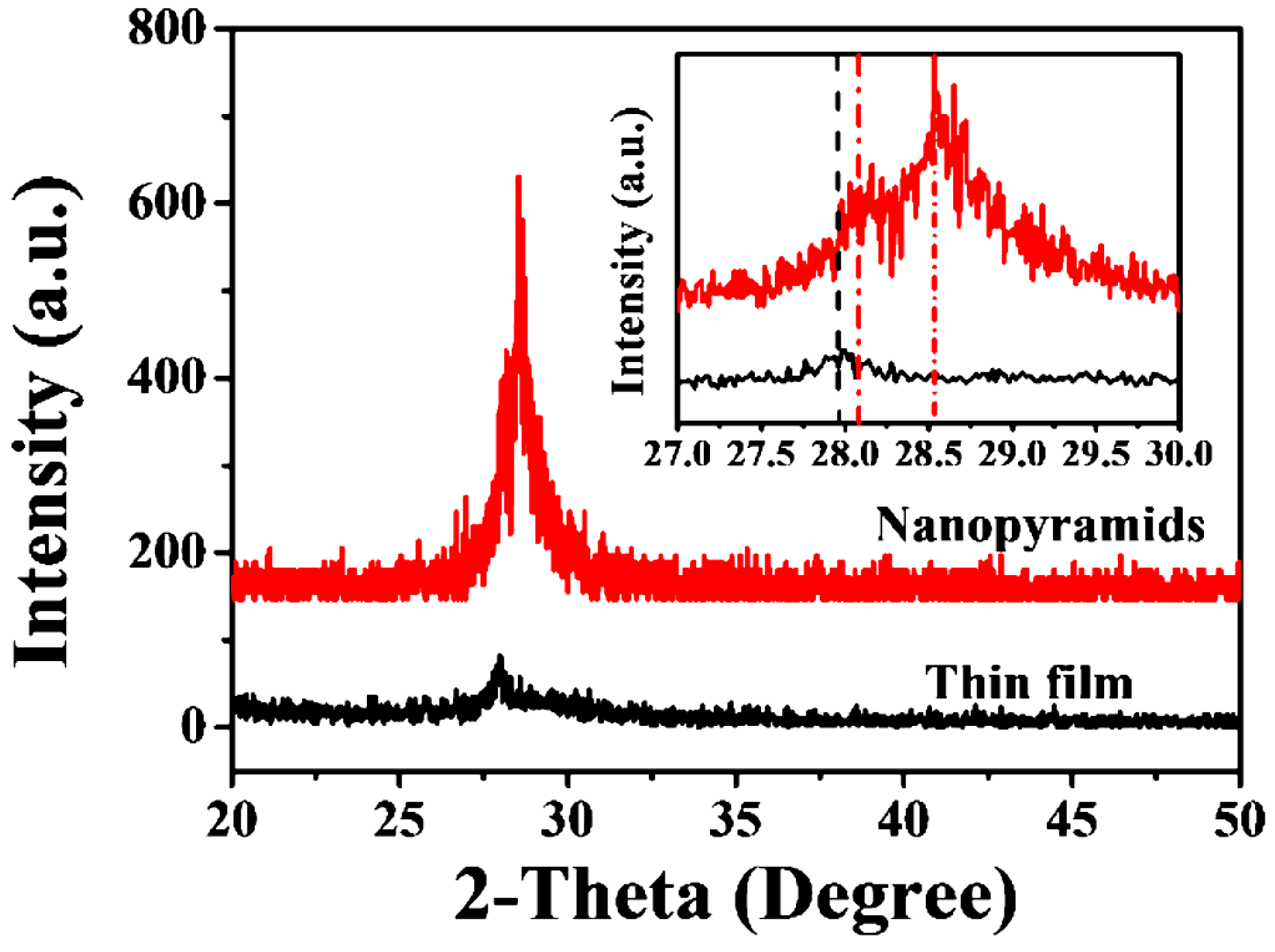
The as-prepared VO2 thin films before and after oxygen-etching treatment were characterized by room temperature XRD measurement (Figure 1). All of the recorded diffraction peaks for the original films obtained at 540 °C in a N2 atmosphere can be assigned to the pure monoclinic phase of VO2 (indexed as VO2 (M1), JCPDS card no. 72-0514, P21/c, a = 0.57 nm, b = 0.45 nm, c = 0.54 nm, and β = 122.61°), in agreement with previous investigations [50,51]. However, after the introduction of oxygen with a controllable amount (0.12 kPa, sample labeled as S-0.12k in the following discussion) during the etching process, a slightly shifted diffraction peak of M1 VO2 (011) (from 27.86° to about 28.01°) and an extra peak at 28.53° were observed. The diffraction pattern at approximately 28.53° could not be assigned directly to any of the vanadium oxide phases, although it was close to the main diffraction peak of the (201) crystalline plane for M2 phase VO2 (JCPDS card no. 33-1441, space group C2/m, a = 0.908, b = 0.576, c = 0.453, and β = 91.3°). The crystallinity increased after the oxygen treatment, as deduced from the decreased full widths at half maximum (FWHM), which were 0.43° and 0.20° for the major diffraction peaks of the plain nanofilm and nanopyramid film, respectively.

Figure 1.
Room temperature X-ray diffraction (XRD) pattern for the VO2 nanofilms deposited on the silicon substrate before and after oxygen injection. The inset shows the enlarged results of the XRD data obtained between 27° and 30° for these films.
The structures and compositions of the films before and after oxygen injection were further confirmed by room-temperature Raman spectra (Figure 2). For the original VO2 films, Raman modes corresponding to M1 phase VO2 were found, with peaks centered at 192, 223, 307, 338, 392, 440, 494, 612, and 816 cm−1 [51,52], respectively. However, after oxygen injection during post-annealing at 540 °C, other modes centered at approximately 271, 432, and 646 cm−1 appeared aside from the modes of the M1 phase of VO2. These modes can be assigned to the metastable M2 phase of VO2, whose Raman modes centered at around 226, 272, 293, 338, 432, 495, and 645 cm−1 [53]. The existence of these Raman modes, especially the characteristic V–V vibration mode at 646 cm−1, indicates that treating the VO2 films with a controllable amount of oxygen produced the VO2 M1/M2 composite structures, agreeing with the XRD results.
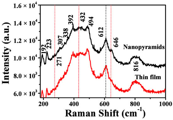
Figure 2.
Room temperature Raman spectra of VO2 nanofilms deposited on the silicon substrate before and after oxygen injection. The excitation power for the Raman spectra was fixed at 1 mW.
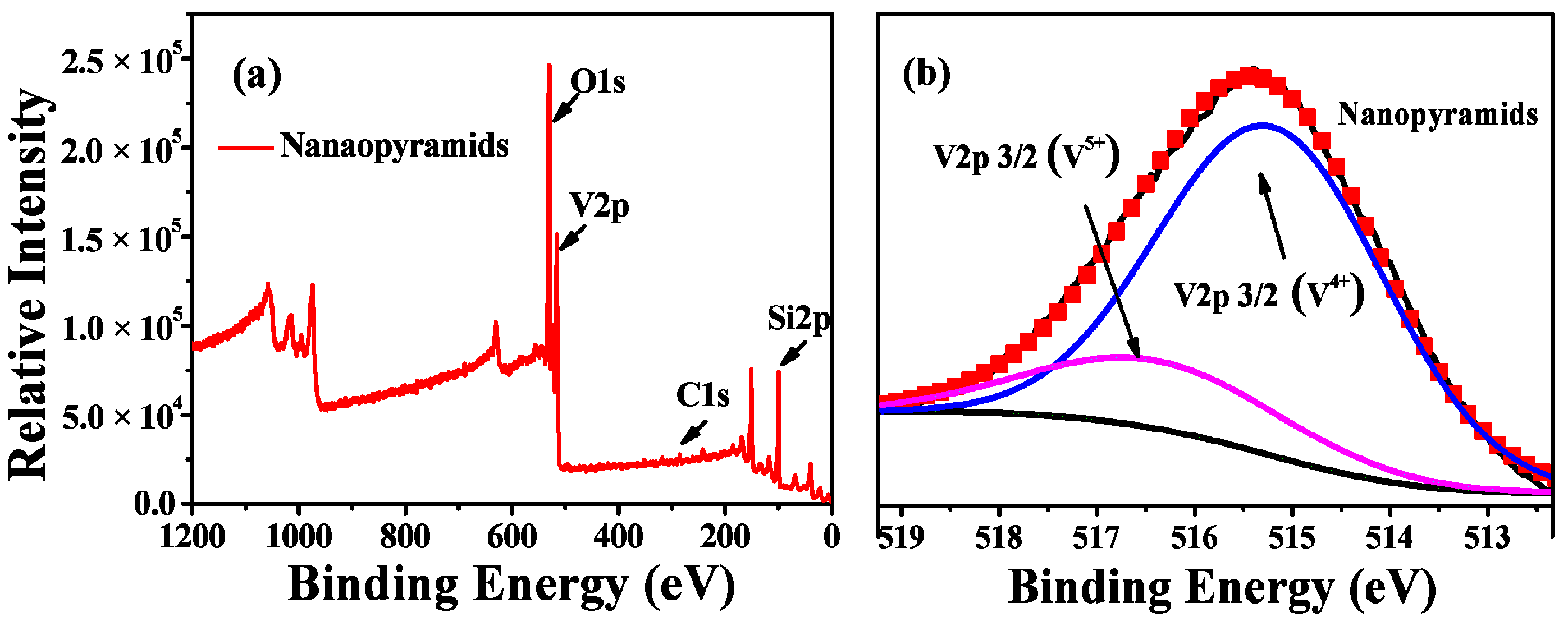
XPS spectra (Figure 3) were further conducted to investigate the compositions and valence states of the vanadium in the films. Surface contamination was removed before the measurements by an Ar ion (1 keV) etching treatment. As shown in a wide-range survey XPS spectrum, a typical prepared sample mainly consisted of vanadium and oxygen, besides the Si signals from the silicon substrate and carbon from the oil residues during pumping by a diffusion pump. The high-resolution XPS (HRXPS) profile of V2p shows the following two major valence states for the vanadium in the pyramidal VO2 films: V4+ with a binding energy of 516.0 eV and V5+ with a binding energy of 517.2 eV [52,54]. The quantitative analysis by peak fitting indicates a composition of VO2.10 for the pyramidal films, which is evidence of the oxidization of the surface of VO2 during the oxygen etching treatment.
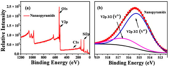
Figure 3.
Wide-range survey XPS spectra (a) and high-resolution XPS profiles (b) of V2p for VO2 nanopyramidal films obtained by oxygen etching at 540° for 1 h.
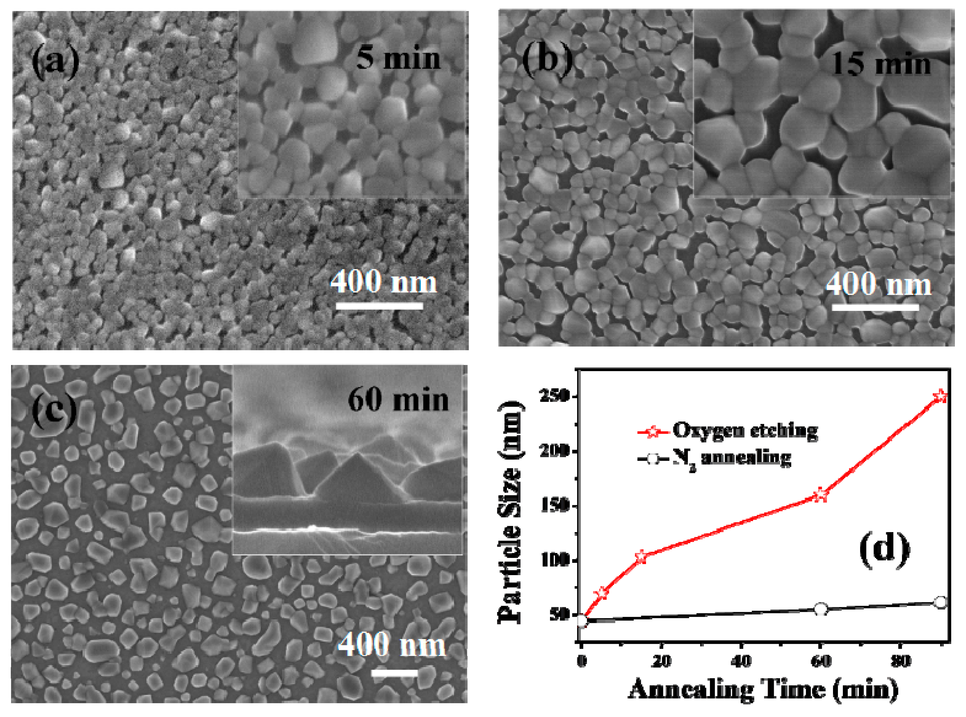
To investigate the influence of oxygen on the morphology evolution of the pyramidal-like VO2 films, FE-SEM observations (Figure 4) were undertaken for the samples treated with oxygen for different times. From the SEM images, one can see that the growth of VO2 nanopyramids in the O2/N2 atmosphere unexpectedly followed the routes of particle top-surface sharpening, size enlarging, and then film structure loosening. Moreover, the growth rate for the oxygen treated sample was much higher than that of the sample annealed in a N2 atmosphere (see the dotted lines in Figure 4d). The particle sizes measured were 71 nm, 110 nm, and 162 nm for the samples treated in oxygen-containing environments for 5 min, 15 min, and 60 min, respectively; while the particle sizes of the samples obtained by annealing in a pure N2 atmosphere were only tens of nanometers. In fact, our further experiments confirmed that for samples treated without oxygen injection (in a N2 atmosphere), significant particle growth could only be observed when annealing at higher temperatures (e.g., above 700 °C), indicating that a new growth pattern was involved in the growth of nanopyramidal VO2 films.

Figure 4.
FESEM morphologies of the VO2 films treated with 0.12 kPa oxygen injection at 540 °C for different times. The annealing times were 5 min (a), 15 min (b), and 60 min (c). The relationship between the particle size and annealing time for N2 annealing and oxygen assisted annealing is shown in (d). The particle size for each film was obtained by randomly counting 100 particles in the SEM images. The insets in (a,b) show the high magnification surface images for the corresponding sample, and the inset in (c) shows the enlarged cross-section image of the sample.
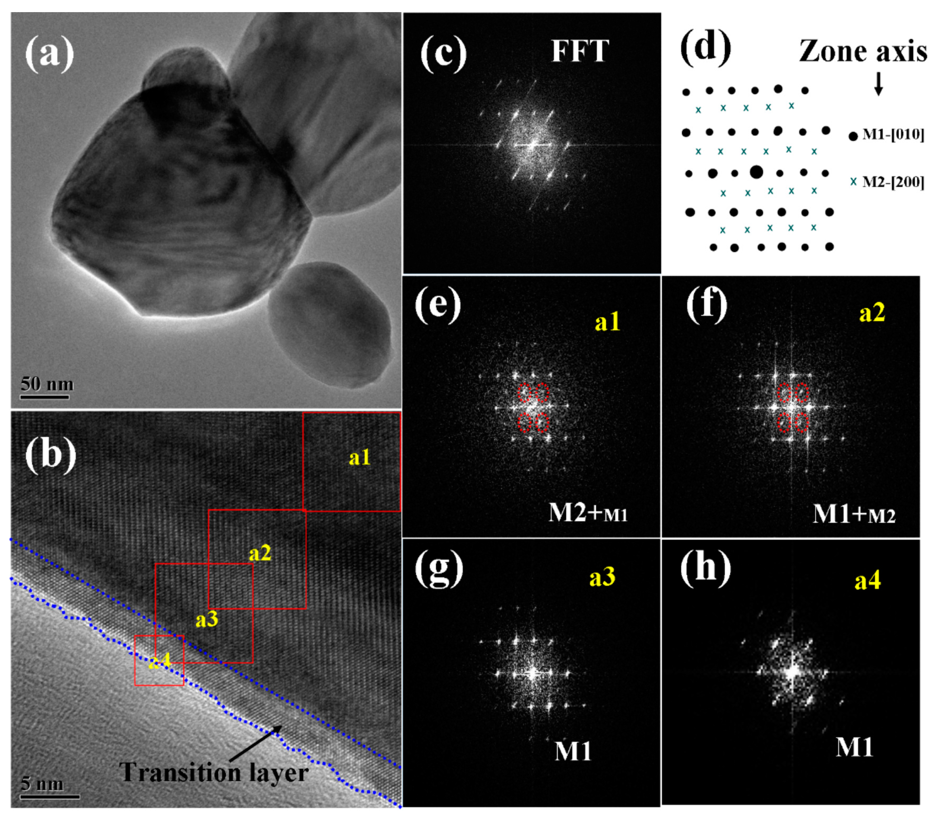
The structure and composition of the pyramid films were further characterized by TEM, high resolution TEM (HRTEM), and fast Fourier transformation (FFT), and the typical results are given in Figure 5. As shown in the low magnification TEM image (Figure 5a), the pyramidal-like morphology for one individual particle can be deduced from the contour stripes. The FFT pattern (Figure 5c) for the total area of Figure 5b indicates that the major structure of the particle is M1 phase VO2 (in the direction of [010]). However, when the FFT patterns were performed in selected small regions, from the outer side to the inner one of the particle (as shown in Figure 5e–h), patterns belonging to M2 phase VO2 (in the direction of [200]) gradually appeared and became stronger and stronger. These results agreed well with the XRD and Raman results, further confirming the formation of composite phases in the pyramidal films.
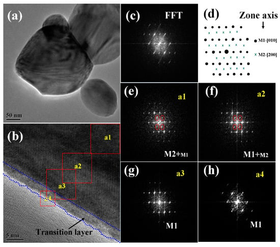
Figure 5.
Low magnification TEM (a), HRTEM (b), and FFT patterns for the total (c) and the selected areas (e–h) of a VO2 nanopyramid particle. The region marked with dotted blue lines in (b) shows the oxygen rich transition layer. (d) shows the demonstration of simulated diffraction patterns for VO2 M1 and M2, from zone axes of M1-[010] and M2-[200], respectively.
As reported by others [53,55,56], the M2 phase is another monoclinic phase of VO2 with a free energy close to that of M1, which can be stabilized by doping [55] or compressive uniaxial stress in the R-[110] direction [56] (equivalent to a tensile strain along the c axis in R phase or a axis in the M1 phase). Considering the XRD results (Figure 1) where the diffraction patterns of M1 phase VO2 (011) (or R phase VO2 (110)) shifted toward high angles, a compressing stress along the R-[110] (or M1-[011]) direction can be expected, which will be favorable for stabilizing the metastable M2 phase. Moreover, the M2 phase has also been reported to be related with the incorporation of V5+ ions in the crystal lattices (by lower valence Cr3+ doping [55], or non-stoichiometric engineering caused by annealing in an oxygen-rich condition [57]). From the high-resolution TEM image in Figure 5b, we could see a distinct thin transition layer on the surface of the pyramidical VO2 nanoparticle, which had a lower contrast and less rigid lattice fringes when compared with the inside VO2 crystals, and the FFT pattern for this layer indicated the structure of M1 phase VO2. Considering the special oxygen treatment and the XPS results, this thin layer, especially for the outer parts, should be composed of slightly oxidized vanadium-oxide species, which works as an intermediate layer between the oxygen environment and the inside VO2 crystals in the annealing process.
When oxygen is injected into the vacuum tube, the top surfaces of the VO2 nanoparticles are expected initially to react with the excess O2 to form oxygen-rich vanadium oxides. The most far-gone form of these oxides is expected to be the highest valence state oxide of V2O5 (Tm, V2O5 = 690 °C), which is highly volatile and can easily evaporate from the surface of the nanoparticles at the annealing temperature of 540 °C (the reaction could be expressed as VO2 (s) + O2 → V2O5 (s/l) → V2O5 (g)). In fact, evaporated V2O5 residues with a characteristic orange color can even be observed at the cold end of the quartz tube. The samples obtained with a higher oxygen injection content in our further experiments also confirmed the existence of V2O5 crystals surrounding the VO2 particles (to be discussed in the following section). An oxygen-related selective etching growth model can be described for the formation of a pyramidal film morphology.
As shown in Scheme 3, when oxygen is injected at a high temperature, the top surfaces of the VO2 nanoparticles react immediately with the excess oxygen to form a thin layer of oxygen-rich vanadium oxides, and the ultimate oxide of V2O5 in the thin layers evaporates partly into the gas phase, which causes the etching of the films. More importantly, due to the diversity in the active energies for different facets of VO2, when the oxygen is injected in a controlled low amount (as discussed for the S-0.12k sample), the reaction speed for different facets will vary. Specifically, because the monoclinic facet (011) is the lowest energy facet in VO2, the other reactive facets may react (or etch) preferentially with O2 to form volatile V2O5 and leave the particle surface. This can cause the preservation of VO2 (011) after etching, which agrees well with the observation that the (011) M1 orientation is highly preferred after oxygen etching.

Scheme 3.
Schematic of etching growth of VO2 nanopyramidal thin films.
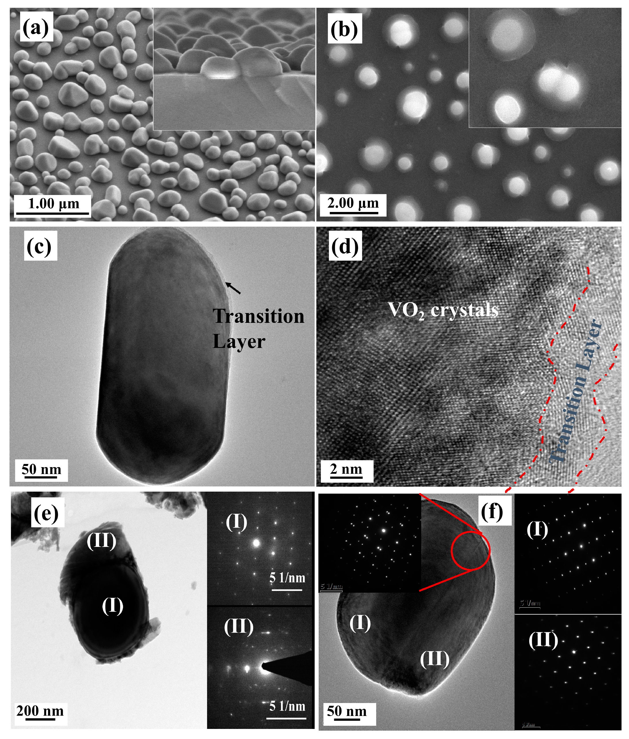
However, for samples with higher oxygen injection contents, the above selective etching patterns were gradually eliminated. Figure 6 shows the SEM and TEM images for the samples treated with higher oxygen injection amounts of 0.20 kPa and 0.24 kPa (labeled as S-0.20k and S-0.24k, respectively). We can see from the SEM images that the top surfaces became much smoother for the S-0.20k film, and even evolved into a spherical (or semi-spherical) morphology for the S-0.24k film, indicating a significant suppression over the facet selective etching growth pattern. Furthermore, for the S-0.24k film, the spherical particles showed a distinct melted droplet-like morphology at the bottom of the etched particles, and large amounts of these particles showed a neck-connected structure (in the inset of Figure 6b).
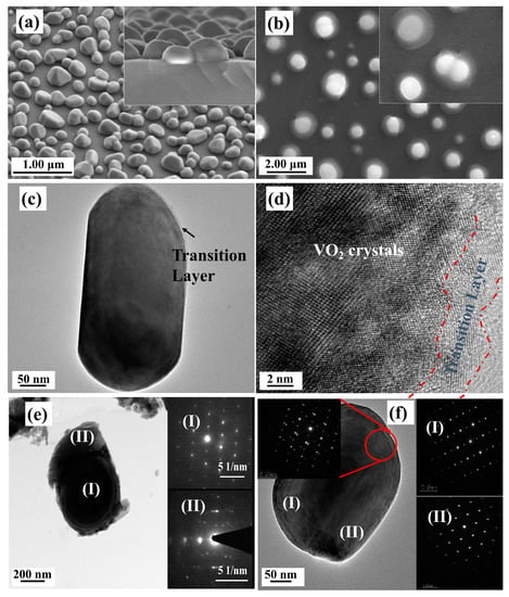
Figure 6.
SEM and TEM characterization of VO2 films annealed at 540 °C for 1 h with 0.20 kPa (a,c,d) and 0.24 kPa (b,e,f) oxygen injection. (a) 30° inclined surface image and a 15° inclined cross-section images (the inset) of a VO2 film annealed with 0.20 kPa oxygen injection; (b) surface image of VO2 film annealed with 0.24 kPa oxygen injection. (c,d) low magnification TEM and HRTEM images of sample a. The region marked with a dotted red line is a transition layer with oxygen rich vanadium oxides. (e,f) TEM images and SAED patterns of two individual particles from sample b, respectively. The SAED patterns in Figure 6e,f were taken from the areas marked in the corresponding low magnification TEM images.
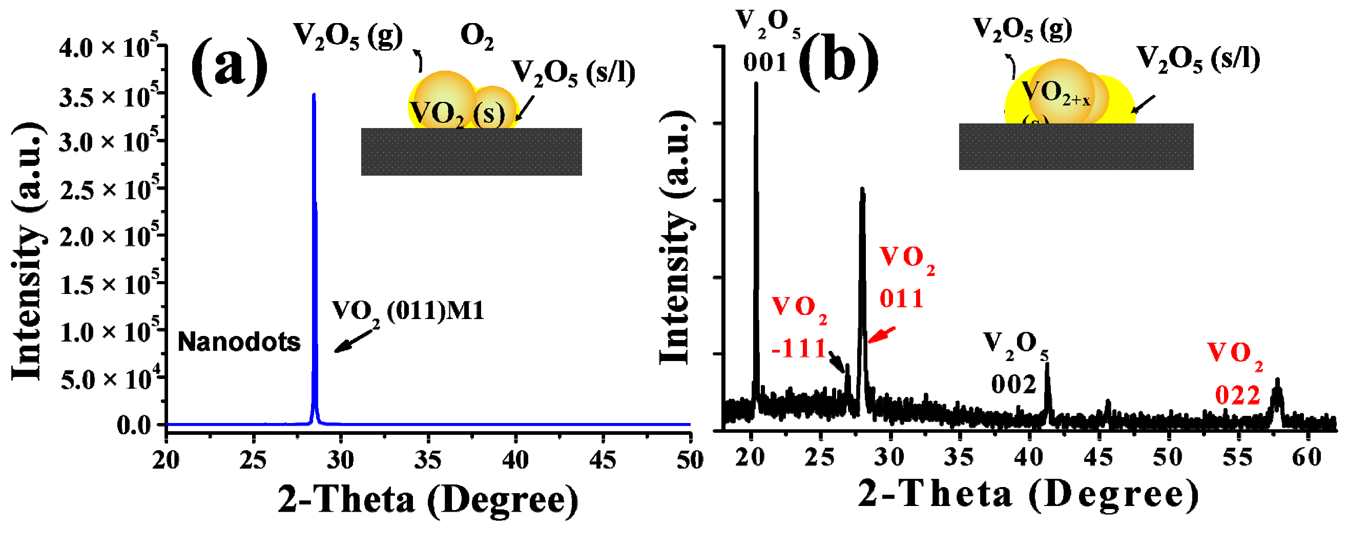
TEM and HRTEM images were further taken to investigate the detailed structures of these films, and the results are given in Figure 6. As shown in Figure 6c,d, the thin transition layers that implied a surface oxidization process could be clearly found on the top surface of the particles for the S-0.20k film, although their lattice fringes were distorted more severely, indicating a much deeper oxidization level and more severe lattice defects with a higher oxygen injection content. For the S-0.24k film, the two distinct structures (in Figure 6b), e.g., the upside nanoparticles and the bottom-laying molten droplets, specifically, were also distinguishable in the TEM images (Figure 6e), and were assigned to the M1 phase VO2 and orthorhombic V2O5 (JCPDS Card File No. 41-1426) by their corresponding selected area electron diffraction patterns (the insets of Figure 6e). Furthermore, the top surface of the connected particles in Figure 6b and its inset were also confirmed as VO2 twin crystals with a M1 phase. Further investigation by XRD characterization indicated that a strongly orientated characteristic along the [011] crystallographic orientation of M1 phase VO2 could be observed for both films, which agreed well with the proposed selective etching mechanism of preserving the stable (011) crystal facets while consuming others during the oxygen treatment. Moreover, when compared with the nanopyramidal films, both films exhibited a smaller FWHM for the (011) diffraction peak, recorded with 0.11° and 0.17° for S-0.20k and S-0.24k, respectively, indicating an increased crystallinity or prompted growth process in this orientation during annealing. However, for the S-0.24k sample, the oxygen concentration applied at 540 °C was too high to stabilize the VO2 crystals, and large amounts were oxidized to be orthorhombic V2O5, which can be seen from the XRD results in Figure 7, in accordance with the TEM observations of the bottom melted droplet-like compounds in Figure 6e.
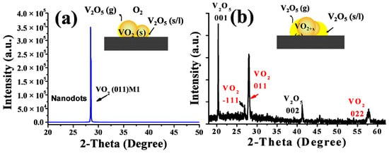
Figure 7.
XRD results for VO2 films that were annealed at 540 °C for 1 h with 0.20 kPa (a) and 0.24 kPa (b) oxygen injection. The insets in the XRD patterns indicate the growth mode of the corresponding films.
All of the above results indicate that the formation of VO2 nanopyramidal structures represents the interplay of the thermodynamic stability of different vanadium oxide phases and the kinetics of vanadium oxidation. With a low oxygen injection content (as discussed for the S-0.12k sample), the reactive facets located on the surfaces of pristine VO2 crystals react immediately with O2 to form thin oxygen rich transition layers, although some of these layers are gradually oxidized into highly volatile oxides of V2O5, resulting in a selective etching growth pattern for the nanopyramidal structures. When a higher content of oxygen was injected (as discussed for the S-0.20k sample), the selective etching process may have been suppressed to a certain extent because of the rapid reaction with a large amount of surrounding oxygen, which could be deduced from the gradually smoothened particle morphology. Furthermore, when the applied oxygen content was too high (as discussed for the S-0.24k sample), large amounts of V2O5, in the vapor phase and/or melted droplet states at the temperature of 540 °C, could be formed aside from the VO2 crystals. The growth patterns for this kind of nanostructure were followed, partly with the routes of oxygen related etching growth as we proposed, although a liquid involved growth mechanism [58,59] should also be considered. After all, by simply controlling the oxygen injection content as discussed above, highly textured VO2 films, especially the nanopyramidal-like nanostructures that have rarely been reported, can be formed, indicating that the current method by oxygen relation etching growth is of competitive potential for the synthesis of nanostructured VO2 films.
Moreover, to explore potential applications of the oxygen etching treated nanostructured VO2 films, field emission (FE) devices were assembled and investigated. The FE device is one of the key features by which nanostructured materials can eject electrons from their surfaces into the vacuum energy level under high electric fields [60,61], and useful applications such as high performance X-ray sources [62,63] can be produced based on the FE properties. According to reports from Yin and Yu [64], VO2 nanobundles exhibit a high field enhancement factor (β) of 1020–1400, which is better than that of Si [65] and Ge nanowires [66], and is comparable to ZnO nanobullets [48] and CdS nanobelts [49]. Furthermore, the Fermi level of VO2 increases distinctly due to the metal-to-insulator phase transition, resulting in a rapid decrease in the work function [64], which makes VO2 materials quite suitable in applications such as temperature-regulated field emission devices. Comparatively, nanopyramidal-like VO2 nanostructures present promising sharp tips that can facilitate electron emission, so a higher field emission performance can be expected.
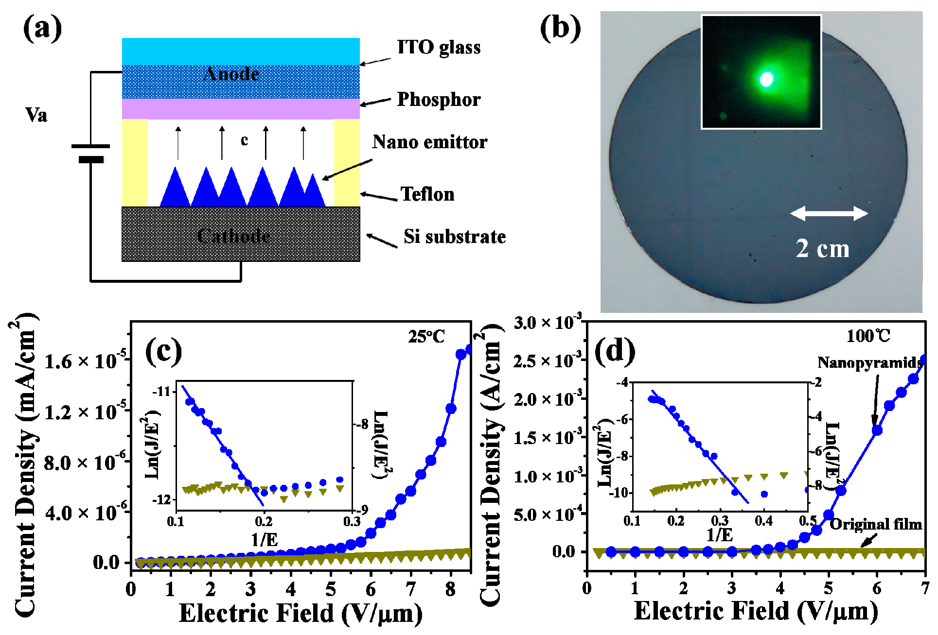
The relationship of the field emission current density J with the applied electric field E (J‒E curves) for the device based on the VO2 thin films before and after the oxygen-etching treatment (corresponding to sample S-0.12k) is shown in Figure 8. The FE measurements were performed at both 25 and 100 °C, respectively. A schematic of the field emission measurement is given in Figure 8a, and a photograph of a large area of VO2 nanopyramidal film (diameter of ~7.6 cm) obtained by this method is given in Figure 8b. As shown in the J‒E curves (Figure 8c,d), the device based on the original VO2 film (the dark yellow lines) showed no or undetectable FE properties at either low or high temperature, while the device made with the nanopyramidal VO2 film after oxygen-etching treatment showed a highly enhanced emission currency at both low and high temperatures, showing an exponential profile versus the applied electric fields. The emission currencies measured at a fixed electric field of 6 V/μm were 1.6 × 10⁻⁶ A/cm2 (or 7.2 × 10⁻⁷ A/cm2) and 1.6 × 10⁻³ A/cm2 (or 1.9 × 10⁻⁵ A/cm2) at the R (or M) state before and after the oxygen-etching treatment, indicating an improvement of nearly 1000 times (or 26 times) in emission currency at the R (or M) state. The increase in emission currency can be expected to originate from the significant changes in film particle morphologies, which can pare away the difficulties of electron field emission for sharp-tipped pyramidal surfaces. Furthermore, the work function of the M1 phase was 0.07 eV, higher than that of the R phase [64], so its improvement in the field emission property was much more significant in the R state after transforming from plain thin films with no FE properties.
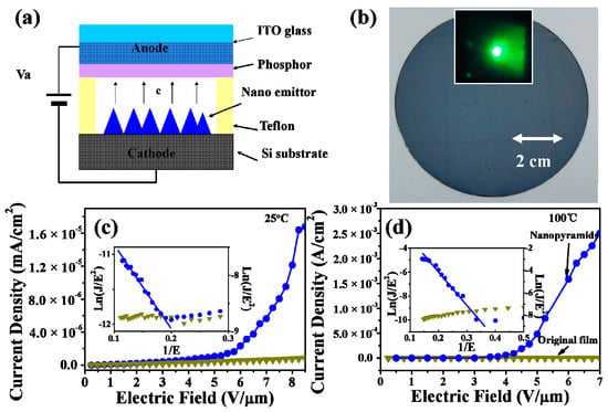
Figure 8.
(a) Schematic of the field emission measurement for VO2 nanopyramid thin films. (b) Photograph of a VO2 nanopyramid thin film deposited on 3-inch silicon substrate. The inset shows a photograph of the green phosphor at an 8 V/μm electrical field. (c,d) J‒E curves for the original (inverted triangle dotted dark yellow lines) and the oxygen etching treated (circle dotted blue lines) VO2 films. The results were measured at 25 (c) and 100 °C (d), respectively. The inset in (c) and (d) shows the Fowler‒Nordheim plots for the corresponding VO2 films.
The Fowler‒Nordheim (F‒N) plots of the ln(J/E2)‒1/E relationship [61] are also shown in the insets of Figure 8c,d. The straight lines fitted in the F‒N plots confirmed the electron field emission characters for the pyramidal VO2 film, which could not be observed for the original plain VO2 thin film. By determining the slop of the F–N plot, one can obtain the data of the field enhancement factor (β), estimated to be about 3810 and 1620 for the M and R states, respectively, which were much higher than those of the reported VO2 nanobundles [64], and comparable with high quality ZnO nanoneedles [67], making the pyramidal VO2 films prepared by the present method attractive for FE applications. Moreover, the feasible and large-area available synthetic strategy reported here can also provide an efficient tool to build a variety of interesting nanoscale VO2 surfaces, which is beneficial for VO2 and other transition metal oxide based device applications.
4. Conclusions
In this paper, we report on an effective wafer-scale oxygen-assisted etching growth strategy for transforming plain VO2 thin films into highly textured nanopyramidal thin films. The controllable amount of oxygen incorporated during the post annealing process reacted rapidly with the reactive VO2 planar surface to form volatile V2O5, which resulted in the effective etching and formation of pyramidal-like VO2 films. The structural investigation indicated that the VO2 films had a composite M1/M2 structure at room temperature. Field emission measurements further showed that the etching process could successfully transform planar VO2 films with no field emission performance into nanopyramidal films with significant field emission performance. The emission currencies at a fixed electric field of 6 V/μm could be improved by 1000 times at the R state before and after the oxygen etching treatment, and the field enhancement factor β reached 3810 and 1620 for the M and R states, respectively, which was quite high amongst all reports. All these results indicate that the technique developed here is an efficient surface building and reconstruction strategy for VO2-based thin films with potential applications in high-performance FE devices.
Author Contributions
Z.Z. and Y.G. conceived the idea. Z.Z. and Y.F. performed the sample preparation, characterization, and measurement of the FE properties and wrote the manuscript. Z.Z., Y.G., Y.F., D.C., and G.S. discussed and analyzed the results. Y.G., D.C., and G.S. revised the manuscript. Z.Z. and Y.G. supervised the whole research work. All authors read and approved the final version of the manuscript.
Funding
This study was supported in part by funding from the National Natural Science Foundation of China (NSFC, Contract No.: 51502268, 51325203, 51574205), the Excellent Young Teacher Development Foundation of Zhengzhou University (Contract No.: 1421320050), the Key Science and Technology Research Projects of Henan Provincial Education Department (Contract No.: 14B430023), Program for Science & Technology Innovation Talents in Universities of Henan Province (14HASTIT011), Special Support Program for High-End Talents of Zhengzhou University (ZDGD13001), and the Plan for Scientific Innovation Talent of Henan Province (154100510003).
Conflicts of Interest
The authors declare no conflict of interest.
References
- Zhang, H.T.; Zhang, L.; Mukherjee, D.; Zheng, Y.X.; Haislmaier, R.C.; Alem, N.; Engel-Herbert, R. Wafer-scale growth of VO2 thin films using a combinatorial approach. Nat. Commun. 2015, 6, 8475. [Google Scholar] [CrossRef] [PubMed]
- Takagi, H.; Hwang, H.Y. An emergent change of phase for electronics. Science 2010, 327, 1601–1602. [Google Scholar] [CrossRef] [PubMed]
- Katzke, H.; Tolédano, P.; Depmeier, W. Theory of morphotropic transformations in vanadium oxides. Phys. Rev. B Condens. Matter 2003, 68, 366–369. [Google Scholar] [CrossRef]
- Goodenough, J.B. The two components of crystallographic transition in VO2. J. Solid State Chem. 1971, 3, 490–500. [Google Scholar] [CrossRef]
- Eyert, V. The metal-insulator transitions of VO2: A band theoretical approach. Ann. Phys. 2002, 11, 650–702. [Google Scholar] [CrossRef]
- Morin, F.J. Oxides which show a metal to insulator transition at the neel temperature. Phys. Rev. Lett. 1959, 3, 34–36. [Google Scholar] [CrossRef]
- Zhang, Z.; Gao, L.H.; Kang, L.; Chen, Z.; Du, J.; Kanehira, M.; Zhang, Y.; Wang, Z.L. Solution-based fabrication of vanadium dioxide on F:SnO2 substrates with largely enhanced thermochromism and low-emissivity for energy-saving applications. Energy Environ. Sci. 2011, 4, 4290–4297. [Google Scholar] [CrossRef]
- Jin, P.; Xu, G.; Tazawa, M.; Yoshimura, K. A VO2-based multifunctional window with highly improved luminous transmittance. Jpn. J. Appl. Phys. Part 2 2002, 41, L278–CL280. [Google Scholar] [CrossRef]
- Li, S.Y.; Niklasson, G.A.; Granqvist, C.G. Nanothermochromics with VO2-based core-shell structures: Calculated luminous and solar optical properties. J. Appl. Phys. 2001, 109, 113515. [Google Scholar] [CrossRef]
- Shadrin, E.B.; Kurdyukov, D.A.; Ilinskiy, A.V.; Golubev, V.G. Conductivity of the opal-VO2 composite at the semiconductor-metal phase transition. Semiconductors 2009, 43, 102–104. [Google Scholar] [CrossRef]
- Pergament, A.; Stefanovich, G.; Berezina, O.; Kirienko, D. Conductivity of tungsten doped vanadium dioxide obtained by the sol-gel technique. Thin Solid Films 2013, 531, 572–576. [Google Scholar] [CrossRef]
- Aliev, V.S.; Bortnikov, S.G.; Badmaeva, I.A. Anomalous large electrical capacitance of planar microstructures with vanadium dioxide films near the insulator-metal phase transition. Appl. Phys. Lett. 2014, 104, 132906. [Google Scholar] [CrossRef]
- Lysenko, S.; Vikhnin, V.; Fernandez, F.; Rua, A.; Liu, H. Insulator-to-metal phase transition and recovery processes in VO2 thin films after femtosecond laser excitation. Phys. Rev. B Condens. Matter 2007, 75, 035104. [Google Scholar] [CrossRef]
- Park, J.; Oh, I.H.; Lee, E.; Lee, K.W.; Lee, C.E.; Song, K.; Kim, Y.J. Structure and magnetism in VO2 nanorods. Appl. Phys. Lett. 2007, 91, 672. [Google Scholar] [CrossRef]
- Lee, K.W.; Kweon, H.; Park, J.; Lee, C.E. Charge and spin dynamics in VO2 nanorods. Appl. Phys. Lett. 2009, 94, 233111. [Google Scholar] [CrossRef]
- Lu, J.P.; Liu, H.W.; Deng, S.Z.; Zheng, M.R.; Wang, Y.H.; van Kan, J.A.; Tang, S.H.; Zhang, X.H.; Sow, C.H.; Mhaisalkar, S.G. Highly sensitive and multispectral responsive phototransistor using tungsten-doped VO2 nanowires. Nanoscale 2014, 6, 7619–7627. [Google Scholar] [CrossRef] [PubMed]
- Chen, S.H.; Yi, X.J.; Ma, H.; Xiong, T.; Wang, H.C.; Ke, C.J. Phase transition VO2 thin films for optical switches. Int. J. Infrared Milli. 2004, 25, 157–163. [Google Scholar] [CrossRef]
- Strelcov, E.; Lilach, Y.; Kolmakov, A. Gas sensor based on metal-insulator transition in VO2 nanowire thermistor. Nano Lett. 2009, 9, 2322–2326. [Google Scholar] [CrossRef] [PubMed]
- Hu, B.; Ding, Y.; Chen, W.; Kulkarni, D.; Shen, Y.; Tsukruk, V.V.; Wang, Z.L. External-strain induced insulating phase transition in VO2 nanobeam and its application as flexible strain sensor. Adv. Mater. 2010, 22, 5134–5139. [Google Scholar] [CrossRef] [PubMed]
- Nakano, M.; Shibuya, K.; Okuyama, D.; Hatano, T.; Ono, S.; Kawasaki, M.; Iwasa, Y.; Tokura, Y. Collective bulk carrier delocalization driven by electrostatic surface charge accumulation. Nature 2012, 487, 459–462. [Google Scholar] [CrossRef]
- Shukla, N.; Parihar, A.; Freeman, E.; Paik, H.; Stone, G.; Narayanan, V.; Wen, H.; Cai, Z.; Gopalan, V.; Engel-Herbert, R.; et al. Synchronized charge oscillations in correlated electron systems. Sci. Rep. 2014, 4, 4964. [Google Scholar] [CrossRef]
- Gurvitch, M.; Luryi, S.; Polyakov, A.; Shabalov, A. Nonhysteretic behavior inside the hysteresis loop of VO2 and its possible application in infrared imaging. J. Appl. Phys. 2009, 106, 104504. [Google Scholar] [CrossRef]
- Yang, T.C.K.; Hung, B.P.P.; Chen, Y.C.; Lai, M.H.; Chung, T.W. Manufacture and characterization of sol-gel V1-x-yWxSiyO2 films for uncooled thermal detectors. Sens. Actuators A 2007, 140, 194–199. [Google Scholar] [CrossRef]
- Yang, Y.; Ko, C.H.; Balakrishnan, V.; Gopalakrishnan, G.; Ramanathan, S. Dielectric and carrier transport properties of vanadium dioxide thin films across the phase transition utilizing gated capacitor devices. Phys. Rev. B Condens. Matter 2010, 82, 205101. [Google Scholar] [CrossRef]
- Wang, D.C.; Zhang, L.C.; Gong, T.D.; Jian, L.K.; Venkatesan, T.; Qiu, C.W.; Hong, M.H. Multiband switchable terahertz quarter-wave plates via phase-change metasurfaces. IEEE Photon. J. 2016, 8, 1–8. [Google Scholar] [CrossRef]
- Skuza, J.R.; Scott, D.W.; Mundle, R.M.; Pradhan, A.K. Electro-thermal control of aluminum-doped zinc oxide/vanadium dioxide multilayered thin films for smart-device applications. Sci. Rep. 2016, 6, 21040. [Google Scholar] [CrossRef]
- Fardad, S.; Das, S.; Salandrino, A.; Breckenfeld, E.; Kim, H.; Wu, J.; Hui, R.Q. All-optical short pulse translation through cross-phase modulation in a VO2 thin film. Opt. Lett. 2016, 41, 238–241. [Google Scholar] [CrossRef]
- Guo, P.; Weimer, M.S.; Emery, J.D.; Diroll, B.T.; Chen, X.; Hock, A.S.; Chang, R.P.; Martinson, A.B.; Schaller, R.D. Conformal coating of a phase change material on ordered plasmonic nanorod arrays forbroadband all-optical switching. ACS Nano 2017, 11, 693–701. [Google Scholar] [CrossRef]
- Lu, X.J.; Chen, A.P.; Luo, Y.K.; Lu, P.; Dai, Y.M.; Enriquez, E.; Dowden, P.; Xu, H.W.; Kotula, P.G.; Azad, A.K.; et al. Conducting interface in oxide homojunction: Understanding of superior properties in black TiO2. Nano Lett. 2016, 16, 5751–5755. [Google Scholar] [CrossRef]
- Jin, P.; Yoshimura, K.; Tanemura, S. Dependence of microstructure and thermochromism on substrate temperature for sputter-deposited VO2 epitaxial films. J. Vac. Sci. Technol. A 1997, 15, 1113–1117. [Google Scholar] [CrossRef]
- Jin, P.; Tazawa, M.; Ikeyama, M.; Tanemura, S.; Macak, K.; Wang, X.; Olafsson, S.; Helmersson, U. Growth and characterization of epitaxial films of tungsten-doped vanadium oxides on sapphire (110) by reactive magnetron sputtering. J. Vac. Sci. Technol. A 1999, 17, 1817–1821. [Google Scholar] [CrossRef]
- Mlyuka, N.R.; Niklasson, G.A.; Granqvist, C.G. Thermochromic multilayer films of VO2 and TiO2 with enhanced transmittance. Sol. Energy Mater. Sol. Cells 2009, 93, 1685–1687. [Google Scholar] [CrossRef]
- Chou, J.Y.; Lensch-Falk, J.L.; Hemesath, E.R.; Lauhon, L.J. Vanadium oxide nanowire phase and orientation analyzed by Raman spectroscopy. J. Appl. Phys. 2009, 105, 034310. [Google Scholar] [CrossRef]
- Qureshi, U.; Manning, T.D.; Parkin, I.P. Atmospheric pressure chemical vapour deposition of VO2 and VO2/TiO2 films from the reaction of VOCl3, TiCl4 and water. J. Mater. Chem. 2004, 14, 1190–1194. [Google Scholar] [CrossRef]
- Sahana, M.B.; Dharmaprakash, M.S.; Shivashankar, S.A. Microstructure and properties of VO2 thin films deposited by MOCVD from vanadyl acetylacetonate. J. Mater. Chem. 2002, 12, 333–338. [Google Scholar] [CrossRef]
- Xu, Y.J.; Huang, W.X.; Shi, Q.W.; Zhang, Y.; Song, L.W.; Zhang, Y.X. Synthesis and properties of Mo and W ions co-doped porous nano-structured VO2 films by sol-gel process. J. Sol-Gel Sci. Technol. 2012, 64, 493–499. [Google Scholar] [CrossRef]
- Song, L.W.; Huang, W.X.; Zhang, Y.B.; Li, D.X.; Shi, Q.W.; Zheng, S.P.; Li, N.; Xu, Y.J. Characteristics of CeOx-VO2 composite thin films synthesized by sol-gel process. J. Mater. Sci. Mater. Electron. 2013, 24, 3496–3503. [Google Scholar] [CrossRef]
- Gao, Y.; Luo, H.; Zhang, Z.; Kang, L.; Chen, Z.; Du, J.; Kanehira, M.; Cao, C. Nanoceramic VO2 thermochromic smart glass: A review on progress in solution processing. Nano Energy 2012, 1, 221–246. [Google Scholar] [CrossRef]
- Kang, L.T.; Gao, Y.F.; Luo, H.J.; Chen, Z.; Du, J.; Zhang, Z.T. Nanoporous thermochromic VO2 films with low optical constants, enhanced luminous transmittance and thermochromic properties. ACS Appl. Mater. Interfaces 2011, 3, 135–138. [Google Scholar] [CrossRef]
- Savo, S.; Zhou, Y.; Castaldi, G.; Moccia, M.; Galdi, V.; Ramanathan, S.; Sato, Y. Reconfigurable anisotropy and functional transformations with VO2-based metamaterial electric circuits. Phys. Rev. B Condens. Matter 2015, 91, 134105. [Google Scholar] [CrossRef]
- Du, J.; Gao, Y.F.; Chen, Z.; Kang, L.T.; Zhang, Z.T.; Luo, H.J. Enhancing thermochromic performance of VO2 films via increased microroughness by phase separation. Sol. Energy Mater. Sol. Cell 2013, 110, 1–7. [Google Scholar] [CrossRef]
- Donev, E.U.; Suh, J.Y.; Lopez, R.; Feldman, L.C.; Haglund, J.R.F. Using a semiconductor-to-metal transition to control optical transmission through subwavelength hole arrays. Adv. Opt. Electron. 2008, 2008. [Google Scholar] [CrossRef]
- Yin, H.H.; Yu, K.; Song, C.Q.; Wang, Z.L.; Zhu, Z.Q. Low-temperature CVD synthesis of patterned core-shell VO2@ZnO nanotetrapods and enhanced temperature-dependent field-emission properties. Nanoscale 2014, 6, 11820–11827. [Google Scholar] [CrossRef] [PubMed]
- Case, F.C. Influence of ion beam parameters on the electrical and optical properties of ion-assisted reactively evaporated vanadium dioxide thin films. J. Vac. Sci. Technol. A 1987, 5, 1762–1766. [Google Scholar] [CrossRef]
- Yuan, N.Y.; Li, J.H.; Lin, C.L. Valence reduction process from sol-gel V2O5 to VO2 thin films. Appl. Surf. Sci. 2002, 191, 176–180. [Google Scholar]
- Della Negra, M.; Sambi, M.; Granozzi, G. Electronic properties and structure of vanadia ultra-thin films grown on TiO2(110) in a water vapour ambient. Surf. Sci. 2001, 494, 213–228. [Google Scholar] [CrossRef]
- Wu, C.Z.; Feng, F.; Feng, J.; Dai, J.; Yang, J.L.; Xie, Y. Ultrafast solid-state transformation pathway from new-phased goethite VOOH to paramontroseite VO2 to Rutile VO2(R). J. Phys. Chem. C 2001, 115, 791–799. [Google Scholar] [CrossRef]
- Gautam, U.K.; Panchakarla, L.S.; Dierre, B.; Fang, X.S.; Bando, Y.; Sekiguchi, T.; Govindaraj, A.; Golberg, D.; Rao, C.N.R. Solvothermal synthesis, cathodoluminescence, and field-emission properties of pure and N-doped ZnO nanobullets. Adv. Funct. Mater. 2009, 19, 131–140. [Google Scholar] [CrossRef]
- Li, L.; Wu, P.; Fang, X.; Zhai, T.; Dai, L.; Liao, M.; Koide, Y.; Wang, H.; Bando, Y.; Golberg, D. Single-crystalline CdS nanobelts for excellent field-emitters and ultrahigh quantum-efficiency photodetectors. Adv. Mater. 2010, 22, 3161–3165. [Google Scholar] [CrossRef]
- Zhang, Y.; Gao, Y.; Kang, L.; Du, J.; Luo, H. Effects of a TiO2 buffer layer on solution-deposited VO2 films: Enhanced oxidization durability. J. Phys. Chem. C 2010, 114, 22214–22220. [Google Scholar] [CrossRef]
- Kang, L.T.; Gao, Y.F.; Luo, H.J. A novel solution process for the synthesis of VO2 thin films with excellent thermochromic properties. ACS Appl. Mater. Interfaces 2009, 1, 2211–2218. [Google Scholar] [CrossRef] [PubMed]
- Zhang, Z.T.; Gao, Y.F.; Chen, Z.; Du, J.; Cao, C.X.; Kang, L.T.; Luo, H.J. Thermochromic VO2 thin films: Solution-based processing, improved optical properties, and lowered phase transformation temperature. Langmuir 2010, 26, 10738–10744. [Google Scholar] [CrossRef] [PubMed]
- Marini, C.; Arcangeletti, E.; Di Castro, D.; Baldassare, L.; Perucchi, A.; Lupi, S.; Malavasi, L.; Boeri, L.; Pomjakushina, E.; Conder, K.; et al. Optical properties of V1-xCrxO2 compounds under high pressure. Phys. Rev. B Condens. Matter 2008, 77, 235111. [Google Scholar] [CrossRef]
- Demeter, M.; Neumann, M.; Reichelt, W. Mixed-valence vanadium oxides studied by XPS. Surf. Sci. 2000, 454, 41–44. [Google Scholar] [CrossRef]
- Marezio, M.; McWhan, D.B.; Remeika, J.P.; Dernier, P.D. Structural aspects of the metal-insulator transitions in Cr-doped VO2. Phys. Rev. B Condens. Matter 1972, 5, 2541–2551. [Google Scholar] [CrossRef]
- Zhang, S.X.; Chou, J.Y.; Lauhon, L.J. Direct correlation of structural domain formation with the metal insulator transition in a VO2 nanobeam. Nano Lett. 2009, 9, 4527–4532. [Google Scholar] [CrossRef] [PubMed]
- Zhang, S.X.; Kim, I.S.; Lauhon, L.J. Stoichiometry engineering of monoclinic to rutile phase transition in suspended single crystalline vanadium dioxide nanobeams. Nano Lett. 2011, 11, 1443–1447. [Google Scholar] [CrossRef]
- Strelcov, E.; Davydov, A.V.; Lanke, U.; Watts, C.; Kolmakov, A. In situ monitoring of the growth, intermediate phase transformations and templating of single crystal VO2 nanowires and nanoplatelets. ACS Nano 2011, 5, 3373–3384. [Google Scholar] [CrossRef] [PubMed]
- Kim, M.H.; Lee, B.; Lee, S.; Larson, C.; Baik, J.M.; Yavuz, C.T.; Seifert, S.; Vajda, S.; Winans, R.E.; Moskovits, M.; et al. Growth of metal oxide nanowires from supercooled liquid nanodroplets. Nano Lett. 2009, 9, 4138–4146. [Google Scholar] [CrossRef] [PubMed]
- Xu, N.S.; Huq, S.E. Novel cold cathode materials and applications. Mater. Sci. Eng. R Rep. 2005, 48, 47–189. [Google Scholar] [CrossRef]
- Fang, X.; Bando, Y.; Gautam, U.K.; Ye, C.; Golberg, D. Inorganic semiconductor nanostructures and their field-emission applications. J. Mater. Chem. 2008, 18, 509–522. [Google Scholar] [CrossRef]
- Gupta, A.P.; Park, S.; Yeo, S.J.; Jung, J.; Cho, C.; Paik, S.H.; Park, H.; Cho, Y.C.; Kim, S.H.; Shin, J.H.; et al. Direct synthesis of carbon nanotube field emitters on metal substrate for open-type X-ray source in medical imaging. Materials 2017, 10, 878. [Google Scholar] [CrossRef]
- Park, S.; Gupta, A.P.; Yeo, S.J.; Jung, J.; Paik, S.H.; Mativenga, M.; Kim, S.H.; Shin, J.H.; Ahn, J.S.; Ryu, J. Carbon nanotube field emitters synthesized on metal alloy substrate by PECVD for customized compact field emission devices to be used in X-ray source applications. Nanomaterials 2018, 8, 378. [Google Scholar] [CrossRef] [PubMed]
- Yin, H.H.; Luo, M.; Yu, K.; Gao, Y.F.; Huang, R.; Zhang, Z.L.; Zeng, M.; Cao, C.X.; Zhu, Z.Q. Fabrication and temperature-dependent field-emission properties of bundlelike VO2 nanostructures. ACS Appl. Mater. Interfaces 2011, 3, 2057–2062. [Google Scholar] [CrossRef] [PubMed]
- Fang, X.S.; Bando, Y.; Ye, C.H.; Shen, G.Z.; Gautam, U.K.; Tang, C.C.; Golberg, D. Si nanowire semisphere-like ensembles as field emitters. Chem. Commun. 2007, 40, 4093–4095. [Google Scholar] [CrossRef] [PubMed]
- Li, L.; Fang, X.S.; Chew, H.G.; Zheng, F.; Liew, T.H.; Xu, X.J.; Zhang, Y.X.; Pan, S.S.; Li, G.H.; Zhang, L.D. Crystallinity-controlled germanium nanowire arrays: Potential field emitters. Adv. Funct. Mater. 2008, 18, 1080–1088. [Google Scholar] [CrossRef]
- Liu, J.P.; Huang, X.T.; Li, Y.Y.; Ji, X.X.; Li, Z.K.; He, X.; Sun, F.L. Vertically aligned 1D ZnO nanostructures on bulk alloy substrates: Direct solution synthesis, photoluminescence, and field Emission. J. Phys. Chem. C 2007, 111, 4990–4997. [Google Scholar] [CrossRef]
© 2019 by the authors. Licensee MDPI, Basel, Switzerland. This article is an open access article distributed under the terms and conditions of the Creative Commons Attribution (CC BY) license (http://creativecommons.org/licenses/by/4.0/).


