Article

The Modulation Effect of MoS2 Monolayers on the Nucleation and Growth of Pd Clusters: First-Principles Study

1
School of Electrical and Electronic Information, Shangqiu Normal University, Shangqiu 476000, China
2
School of Physics and Engineering, Zhengzhou University, Zhengzhou 450001, China
3
Faculty of Physics and Electronic Sciences, Hubei University, Wuhan 430062, China
*
Authors to whom correspondence should be addressed.
Nanomaterials 2019, 9(3), 395; https://doi.org/10.3390/nano9030395
Submission received: 11 January 2019 / Revised: 22 February 2019 / Accepted: 1 March 2019 / Published: 8 March 2019

Abstract

:
The geometries, electronic structures, adsorption, diffusion, and nucleation behaviors of Pdn (n = 1–5) clusters on MoS2 monolayers (MLs) were investigated using first principles calculations to elucidate the initial growth of metal on MoS2. The results demonstrate that Pd clusters can chemically adsorb on MoS2 MLs forming strong Pd–S covalent bonds with significant ionic character. We investigated the initial growth mode of Pd clusters on MoS2 monolayers and found that Pdn clusters tend to adopt pyramid-like structures for n = 4–5 and planar structures lying on MoS2 substrates for n = 1–3. It can be explained by the competition between adsorbate–substrate and the intra-clusters’ interactions with the increasing coverage. Compared with pristine MoS2 MLs, the work function was reduced from 5.01 eV upon adsorption of Pd monomer to 4.38 eV for the case of the Pd5 clusters due to the charge transfer from Pd clusters to MoS2 MLs. In addition, our calculations of the nucleation and diffusion behaviors of Pd clusters on MoS2 MLs predicted that Pd is likely to agglomerate to metal nanotemplates on MoS2 MLs during the epitaxial stacking process. These findings may provide useful guidance to extend the potential technological applications of MoS2, including catalysts and production of metal thin films, and the fabrication of nanoelectronic devices.

1. Introduction

In recent years, two-dimensional (2D) layered transition metal dichalcogenides (TMDs), particularly MoS2, exhibiting excellent electronic and optical properties, have drawn great attention due to their potential applications in flexible nanoelectronics, photonic devices, memory devices, etc. [1,2,3,4]. A series of experimental and theoretical studies have confirmed that MoS2 monolayers (MLs) decorated with metal nanoparticles (NPs) could potentially extend its functionalities as novel catalysts, spintronic devices, and thermoelectric and photoelectric materials, which is owing to the unique size-dependent properties of metal nanoparticles [5,6,7,8]. For instance, Chen et al. [5] reported the metal clusters (Pd, Pt, and Ag) supported on MoS2 MLs tend to display excellent electrocatalytic activity compared to those on graphene. Fu et al. [6] found that Au nanoparticles on two-dimensional MoS2 nanosheets can be used to fabricate an attractive alternative photoanode for efficient photoelectron chemical miRNA detection. Recently, Burman and co-workers [7] successfully fabricated Pt decorated MoS2 nanoflakes, and further confirmed its potential application as the sensing layer of an ultrasensitive resistive humidity sensor. Besides, Li et al. [9] reported that Au NPs imposed remarkable p-doping effects onMoS2 transistors, which implied that a controllable method of metal NP decoration provides an effective way to design future optoelectronic devices. Furthermore, Guo et al. [10] used 2D MoS2 effectively decorated with Au nanoparticles to improve the performance of flexible thermoelectric materials, which may become an alternative material for wearable thermoelectric devices. In addition, the MoS2–Pd nanoparticle hybrid structure was used to engineer the oxide/electrode interface of hafnium oxide (HfOx)-based metal oxide-based, resistive random-access memory, which has huge potential application in the field of data storage and wearable electronics [11].
Meanwhile, both experimental and theoretical studies have revealed that the surfaces of MoS2 MLs with graphene-like structures can play an active role as a host surface for the clusterization and nucleation characteristics of transition metal atoms. Huang and co-workers [12] demonstrated that MoS2 nanosheets can be used to direct the epitaxial growth of Pd, Pt, and Ag nanostructures by wet-chemical synthetic method under ambient conditions in experiments. Song et al. [13] studied the nucleation and growth dynamics of Au nanoparticles on MoS2 nanoflakes by in situ liquid-cell transmission electron microscopy (TEM). In order to design more efficient and less expensive catalysts, the evolution of morphology and epitaxial growth of Pt NPs on MoS2 (001) surfaces was systematically analyzed by density functional theory study [14]. Recently, Jiang and co-workers [15] proposed that 2D Fe/MoS2 heterostructures constructed by deposition of Fe atoms on MoS2 exhibits robust half-metallic magnetism and possesses robust ferromagnetic and half-metallic properties with 100% spin-filter efficiency based on first-principles calculations. Similarly, Cooley et al. [16] showed that graphene/MoS2 heterostructures can be used as templates to grow stable clusters lying planar to the surface, as well as to prepare monoatomic layers of ordinary metals.
It is also known that the nature of metal–semiconductor interfaces plays a more important role than MoS2 MLs themselves in MoS2-based optoelectronics and nanoelectronics [17]. Motivated by the high work function of Pd and the small lattice mismatch of Pd and MoS2, Pd can be used as the p-type metal contact on MoS2 to modify the Schottky barrier height (SBH) and the charge carrier injection rates. Fontana et al. [18] have observed that MoS2-based transistors show hole-doping and electron-doping behaviors when Pd and Au are used for source and drain contacts, respectively, and the formation of Schottky junctions at contact interfaces remarkably induced a clear photovoltaic effect. Later work highlighted an epitaxial growth mode of Pd deposition on MoS2 bulk surface and a strong band bending effect and high contact resistance were observed for the Pd/MoS2 interface [19]. Although metal contact engineering is a very useful avenue for building high-performance MoS2-based devices, there is little research on how MoS2 MLs modulate the nucleation and growth processes of Pd NPs and which further explores the nature of Pdn/MoS2 interfaces. Above all, it is crucial to explore the formation and diffusion properties of Pd clusters on MoS2 MLs and to investigate the modulation effect of MoS2 surfaces on the growth of Pdn clusters for the sake of improving deposition technological applications at the device level.
In this work, we aim to systematically investigate the adsorption behaviors including geometries, relative stability, and electronic properties of Pdn (n = 1–5) clusters on MoS2 MLs, and the diffusion behaviors of Pdn (n = 1–5) clusters on MoS2 are discussed using density functional theory (DFT) calculations. The rest of the paper is organized as follows. In Section 2 we briefly describe the calculation method used. In Section 3 we report our results and discussions including the structures, relative stabilities, and the electronic properties of Pd clusters supported by MoS2 MLs. Meanwhile, in order to better understand the role of MoS2 surfaces during the nucleation of Pd clusters, the diffusion characteristics of Pdn (n = 1–5) clusters are discussed in detail. The conclusions are given in the last section.

2. Computational Details

The geometries, electronic structures, and diffusion characters of Pdn (n = 1–5) clusters absorbed at MoS2 MLs were carried out with the first-principles calculations based on density functional theory (DFT) under the generalized gradient approximation (GGA) as implemented in the VASP code [20,21]. A plane wave basis set with the projector-augmented plane wave (PAW) was performed to describe the ion–electron interaction [22]. The plane-wave cutoff corresponding to a kinetic energy of 450 eV was adopted. The k-point meshes were generated according to the Monkhorst–Pack scheme [23] and 9× 9 × 1 mesh was used to sample the supercell which consisted of 4 × 4 MoS2 units in the calculations. In order to prevent the interactions between neighboring slabs, a thick vacuum layer of more than 15Å was adopted in a direction perpendicular to the surface. During structural relaxation, all the atomic coordinates (including Mo, S, and Pd) were fully relaxed until the Hellmann–Feynman forces were smaller than 0.01 eV/Å.
To describe quantitatively the energetic trends of adsorbed Pd clusters on the MoS2 ML and to further explore the modulation of MoS2 substrate on the growth mechanism of Pd clusters, we introduce adsorption energy EA, binding energy EB, and intra-cluster binding energy EIB, which are defined as the following:
(1)
The adsorption energies EA,
E A = [ E MoS 2 + E Pd n E t o t Pd n / MoS 2 ] / n ,
where E t o t Pd n / MoS 2 and E MoS 2 are the total energies of the MoS2 monolayer with and without Pdn clusters, E Pd n is that of the floating Pdn clusters consisting of n Palladium atoms. EA can be used to describe quantitatively the strength of the adsorbate–substrate interaction.
(2)
The binding energy EB,
E B = [ E MoS 2 + n E Pd E t o t Pd n / MoS 2 ] / n ,
where E Pd is the total energy of an isolated Palladium atom in a cubic supercell of 20 Å × 20Å × 20Å. The binding energy EB reflects the relative stability of the Pdn clusters supported by the MoS2 ML.
(3)
The intra-cluster binding energy EIB,
E I B = E B E A ,
which could qualitatively reflect the strength of the Pd–Pd interactions. In order to compare directly, all considered energy terms were normalized with respect to the number of Pd atoms, given per adatom.
To get insight to the nucleation mechanism and growth mode of Pd clusters, we also calculated the diffusion properties of Pdn (n = 1–5) clusters supported by the MoS2 ML. The diffusion barrier and transition states were determined from the minimum energy pathway by employing the climbing-image nudged elastic band (NEB) method [24,25]. All geometries were optimized until the maximum force in every degree of freedom was less than 0.005 eV Å.

3. Results and Discussions

3.1. Geometries and Stabilities for Pdn (n = 1–5) Adsorbed at MoS2 ML

In order to understand the adsorption properties of Pdn (n =1–5) clusters and explore the nucleation mechanism and initial growth of Pd nanoparticles on MoS2 MLs, it is essential to identify the structural and electronic properties of pure MoS2 ML for comparison. 
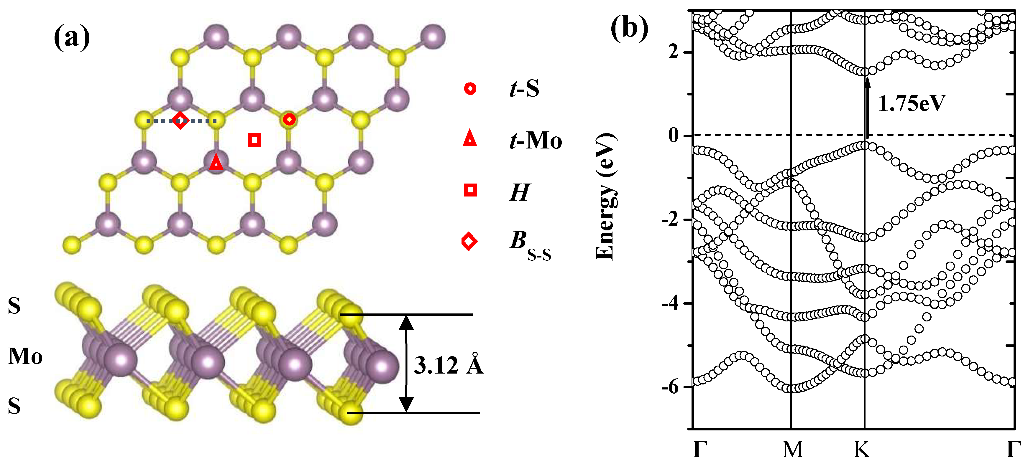
Figure 1a shows the top and side view of a 4 × 4 supercell of the MoS2 ML; the calculated results show that the thickness of the MoS2 ML was 3.14 Å and the bond length of the S–Mo was 2.84 Å, which is consistent with previous studies [26,27]. Besides, we calculated the band structures of the MoS2 ML as shown in Figure 1b. The calculated results indicate that the MoS2 ML presented semiconducting character with a direct gap of 1.75 eV at the K point, which is in good agreement with the previous theoretical results of 1.70 eV [28] and experimental results of 1.80 eV [29].
We first investigated the geometries and adsorption properties of a single Pd adatom on the MoS2 ML. For the case of Pd monomer, we considered the binding of Pd on four high-symmetry sites: the hollow (H) site at the center of a hexagon, the top site directly above Mo (t-Mo) and S (t-S), and the bridge (BS–S) site at midpoint of the S–S bond, as shown in Figure 1a. It is known that the larger the adsorption energy EA, the stronger the interaction between the adsorbate and substrate. Table 1 lists the structural parameters and adsorption energies for all considered adsorption configurations of Pd monomer adsorbed at the MoS2 ML. The calculated results show that the t-Mo site with the adsorption energy of 2.16 eV was the most energetically favorable location, which is consistent with previous studies [26,30]. The Pd monomer adsorbed at the t-S and H sites were 0.57 and 0.37 eV, respectively, less stable than that of the t-Mo adsorption configuration. Our calculated results show that Pd monomer located at the BS-S site finally relaxed to the t-Mo configuration, which indicates that Pd monomer adsorbed at the BS-S site was unstable. As summarized in Table 1, Pd bonds to the surrounding S atoms with a bond length of 2.34, 2.42, and 2.18 Å for the considered adsorption configurations of t-Mo, t-S, and H, respectively, which are comparable with those in two types of PdS2 monolayer with values of 2.34 and 2.40 Å [31]. The distances between Pd and nearest neighboring Mo are 2.34, 2.30, and 2.26 Å for three considered configurations, which are mainly resulting from the different adsorption sites. The Pd monomers located at 1.33, 1.59, and 2.19 Å higher than the underlying MoS2 surface for three considered adsorption configurations, which is consistent with the decreased trend for the calculated adsorption energies from the t-Mo to t-S configuration.
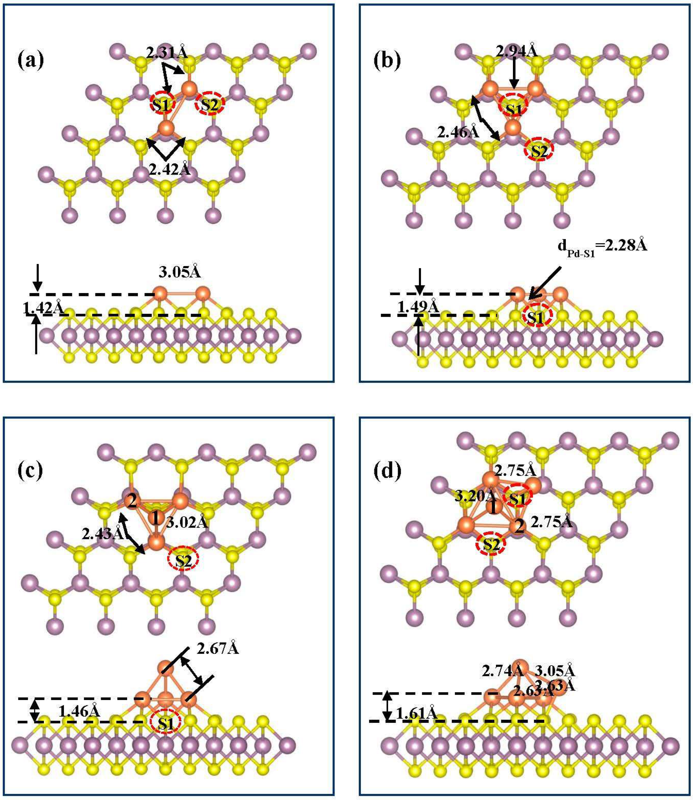
We have chosen several initial configurations to search the most stable configurations of Pdn (n = 2–5) clusters adsorbed at the MoS2 ML, which is shown in Figure 2. The calculated structural parameters and adsorption, binding, and intra-cluster binding energies for the lowest energy configurations of Pdn (n = 1–5) adsorbed on the MoS2 ML are summarized in Table 2. The most preferential configuration of Pd dimer adsorbed at the MoS2 ML was that two Pd atoms both adsorbed at the top of Mo, and they were separated by 3.05 Å, which was smaller than the calculated lattice constant of MoS2 ML, as shown in Figure 3a. For the cases of Pd3 cluster adsorbed at MoS2 ML, the calculated results show that the t-(Mo)3-S configuration with the largest adsorption energy of 1.44 eV presents higher stability than the t-(Mo)3-h configuration due to the extra binding of S1 atom, in which Pd trimer stands in a plane parallel to the MoS2 surface. Besides, it is not surprising that the considered t-(Mo)3-L with three Pd atoms in a line adsorbed at the top of Mo is higher in energy than the triangular islands because of the decrease in the number of intra Pd–Pd bonds. The average bond length of Pd–Pd and the height of Pd3 cluster above the MoS2 surface are 2.94 and 1.49 Å, respectively. The Δ–(Mo)3 structure where two Pd atoms were located at the t-Mo sites and the third one was located at the bridge site of the two Pd atoms was also considered for the case of the Pd3 cluster. However, different from the case of Pt3 on MoS2 ML, such vertical configuration is unstable as it is about 0.65 eV less stable than the t-(Mo)3-S configuration. For the case of Pd tetramers adsorbed at MoS2 surface, we considered three possible configurations, including aplanar-(Mo)4 (four Pd atoms located at the t-Mo site, not shown here), pyramid-like t-(Mo)4-h, and t-(Mo)4-S configurations. The computed results show that the most favorable structure is t-(Mo)4-h (shown in Figure 2c) for Pd tetramer adsorbed at the MoS2 ML, implying the growth mechanism transitions from a two-dimensional (2D) to a three-dimensional (3D) mode from the formation of Pd4 cluster. Based on the most stable configuration of Pd4 tetramers supported by the MoS2 ML, we considered three initial geometries for Pd pentamer. After full structural optimization, the most stable structure was asquare pyramid t-(Mo)5, shown in Figure 2d, which could be obtained by adding one additional Pd atom adsorbed at a neighboring t-Mo site with respect to the t-Pd4-h configuration.
From the above calculations, it is clear that the palladium clusters are energetically preferred to lying planar to the surface for the initial growth of Pdn clusters on MoS2 ML at very low coverage (from Pd1 to Pd3). With increasing the coverage, the Pdn clusters immediately form islands clusters, such that the morphology of t-(Mo)4-h and t-(Mo)5-h are the most stable configurations for Pd tetramer and pentamer, respectively. Therefore, under situations dominated by the thermodynamic effects, the clusters with planar structures may be expected to only appear in the very early growth stage and the size of these clusters are very small (e.g., Pd2 and Pd3), which is immediately followed by the Vomler–Weber growth mechanism.
In our previous study on the initial growth of Pdn/NiAl(110) [32], we reported that small-size Pdn (n = 1–5) clusters favor the planar structures on the NiAl(110) surface, which was explained by the stronger interaction between Pdn clusters and NiAl substrate than the interaction among Pd adatoms in clusters. In order to explore the modulation of MoS2 substrate on the growth mechanism of Pdn clusters, it is crucial to understand the evolutions of the metal–metal and metal–slab interactions with the increase of cluster size. We summarize the adsorption, binding, and intra-cluster binding energies as well as structural parameters for the most stable structures of Pdn (n = 1–5) adsorbed on the MoS2 ML in Table 2. It was found that the adsorption energies, EA, decreased from 2.16 to 0.86 eV when the Pd coverage increased from Pd1 to Pd5 clusters, which indicates the strength of the interactions between the Pdn (n = 1–5) clusters and MoS2 gradually weakened. The results are reasonable since the height of Pd clusters above MoS2 increases from Pd monomer to Pd3 cluster with planar structures. For the case of pyramid-like structures, Pd5 waslocated at 0.03 Å higher than that of Pd4 above the MoS2 ML as listed in Table 2; however, the additional Pd–Pd bonds weakened the Pd–S bonds resulting in less stability of Pd5 cluster. The binding energy, EB, that reflects the relative stability of the Pdn (n = 1–5)/MoS2 system, gradually increased from 2.21 eV for Pd2 to 2.38 eV for Pd5, which indicates the relative stability of larger Pd clusters adsorbed at the MoS2 ML was higher than that of smaller ones. With the increase of Pd coverage (from Pd2 to Pd5), the intra-cluster binding energy EIB rapidly increased from 0.37 to 1.52 eV, which suggests that the interaction among the Pd adatoms in the Pd5 cluster was stronger than those of smaller ones. Besides, it was noticeable that the EIB was larger than EA for Pd4 and Pd5, which indicated that intermetallic Pd–Pd bonds in clusters were stronger than the bonds between Pd and surrounding S or Mo. This can be used to explain the fact that the most stable structures for Pd4 and Pd5 started to appear around the three-dimensional structures with smaller Pd–Pd bond lengths (about 2.63 Å). Compared with a previous study on Pdn cluster/graphene [33], in which size-selected monodisperse nanoclusters were identified by scanning tunneling microscopy, Pdn clusters supported by MoS2 are more stable due to larger binding energies and shorter distance between Pdn and MoS2 substrate, which indicated that the MoS2 ML was inert and an ideal template for deposition of the metal NPs to some extent.

3.2. Electronic Properties of Pdn (n=1–5)/MoS2 Monolayer

In order to better understand and control how the deposition of Pd clusters affect the structure and electronic properties of MoS2, we calculated the density of states (DOS) of MoS2 ML with and without the adsorption of Pdn (n = 1–5) clusters shown in Figure 3. It is clear that the 4d states of isolated Pd atom was very sharp at 0.35eV, while 4d states of Mo hybrids with the 3p states of neighboring S atoms for pure MoS2 ML. Upon the adsorption of Pd monomer on MoS2 (Figure 3b), the band gap decreased to about 1.09 eV, which is mainly attributed to the hybridization of the 4d states of Pd atoms with 4d states of underlying Mo and 3p states of the nearest surrounding S at 0.50 eV below Fermi level. For the case of Pd dimmer adsorbed at MoS2 ML (Figure 3c), a gap state emerged at the 0.80 eV above the Fermi level, which resulted from the hybridizations between Pd atoms and the nearest-neighboring Mo and S atoms. For the case of Pd3 cluster, the partial density of states (PDOS) of three Pd adtoms were similar due to the identical atomic environments as shown in Figure 3d. We found that Pd adatoms hybridize more strongly with the S atom located at the hollow site of the Pd trimer (labeled by S1 in Figure 2b) than the nearest-surrounding S atoms (labeled by S2 in Figure 2b) at −0.80 eV. For the case of the Pd4 and Pd5 clusters with pyramid-like geometries (Figure 3e–f), the DOS of the topmost Pd adatoms labeled as Pd4-1 and Pd5-1 (located at the second layer of clusters) in Figure 2c were relatively localized compared with those of the underlying Pd (labeled by Pd4-2 and Pd5-2 in Figure 2d, which were located at the first layer of the clusters), which indicated that the electronic properties of the topmost Pd were hardly affected by the MoS2 substrate. The calculated results also show that the gap state located above the EF was shifting close to 0 eV from the Pd3 to Pd5 clusters, which caused the band gap to decrease from 0.70 eV of the Pd3/MoS2 system to 0.19 eV of the Pd5/MoS2 system.

3.3. Charge Redistribution and Work Functions

In order to analyze the character of bonds between adsorbates and MoS2 substrate as well as the charge redistribution of MoS2 upon the adsorption of Pd clusters, we calculated and analyzed the electron density difference, which is defined as Δ ρ = ρ Pd n MoS 2 ρ MoS 2 ρ Pd n , where ρ Pd n MoS 2 is the charge density of total system, ρ MoS 2 and ρ Pd n are the charge densities of pristine MoS2 ML and the free-floating Pd clusters in the frozen geometry they adopted on the Pdn/MoS2 system, respectively. 
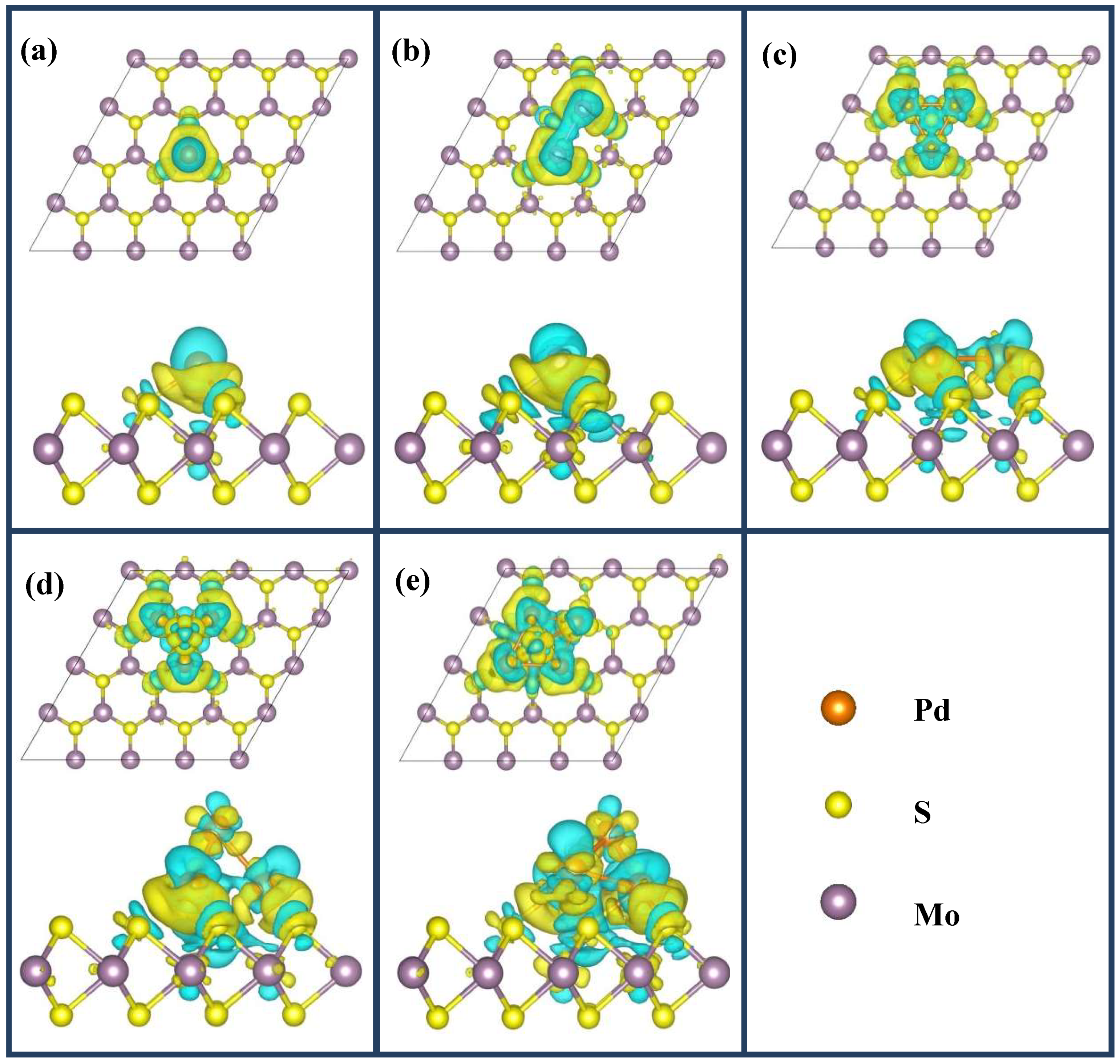
Figure 4 shows the corresponding difference in electron densities for all considered optimized stable configurations, yellow and blue region represent charge accumulation and charge loss, respectively. As shown in Figure 4, the charge redistributions upon the deposition of Pdn cluster mainly involved Pd clusters and surrounding S and Mo atoms, which imply strong charge transfers between the Pdn (n = 1–5) clusters and MoS2 substrate. It is clear that there was strong electron density accumulation between Pd atoms and nearest-neighboring S atoms, which indicates that the bonds between Pd adatoms and surface S atoms present a covalent bond with partial ionic features. There are depletion regions close to the Pd atoms along the bond directions of Pd–S, which can be explained by the stronger electronegativity of S than Pd. For the cases of Pd2 and Pd3 clusters, the Pd atoms highly hybrid with the center-S (labeled as S1 in Figure 2). It is also observed that the characteristics of Pd–Pd bond remain strong metallic upon Pd clusters supported by MoS2 ML. However, for the cases of the Pd4 and Pd5 clusters (Figure 4d,e), it is surprising that strong electron density accumulation was found for the topmost Pd atoms (such as Pd4-1 and Pd5-1), which indicates that the top Pd atoms directly receive charge from the underling Pd layers rather than losing charge to the MoS2 substrate.
To further give a detailed insight into the charge transfer, we also calculated the atomic populations for the most favorable configurations of Pd clusters adsorbed at the MoS2 ML, as summarized in Table 3. Upon Pd adatoms adsorbed at the t-Mo site, Pd adatoms lost about 0.26e to the MoS2 ML by Bader analysis, which suggested Pd–S bonds exhibited a relatively significant ionic bonding component, as illustrated by the substantial charge density difference between Pd and neighboring S atoms shown in Figure 3a. Similarly, Pd adatoms in dimer and trimer averagely contributed about 0.20 and 0.18e to the MoS2 ML, respectively. However, in the cases of Pd4 and Pd5 clusters with pyramid-like geometry, Pd atoms in the first layer and second layer of the clusters behave in a different way. The Pd atoms in the second layer of the cluster (Pd4-1 and Pd5-1) obtained charge, while the Pd atoms of the first layer lost charge. This result is in good agreement with the phenomenon of charge accumulation near the topmost Pd atoms as shown in Figure 4d,e. Therefore, it is not surprising that the MoS2 slabs obtained less charge from Pd4 and Pd5 clusters than that of the Pd3 cluster.
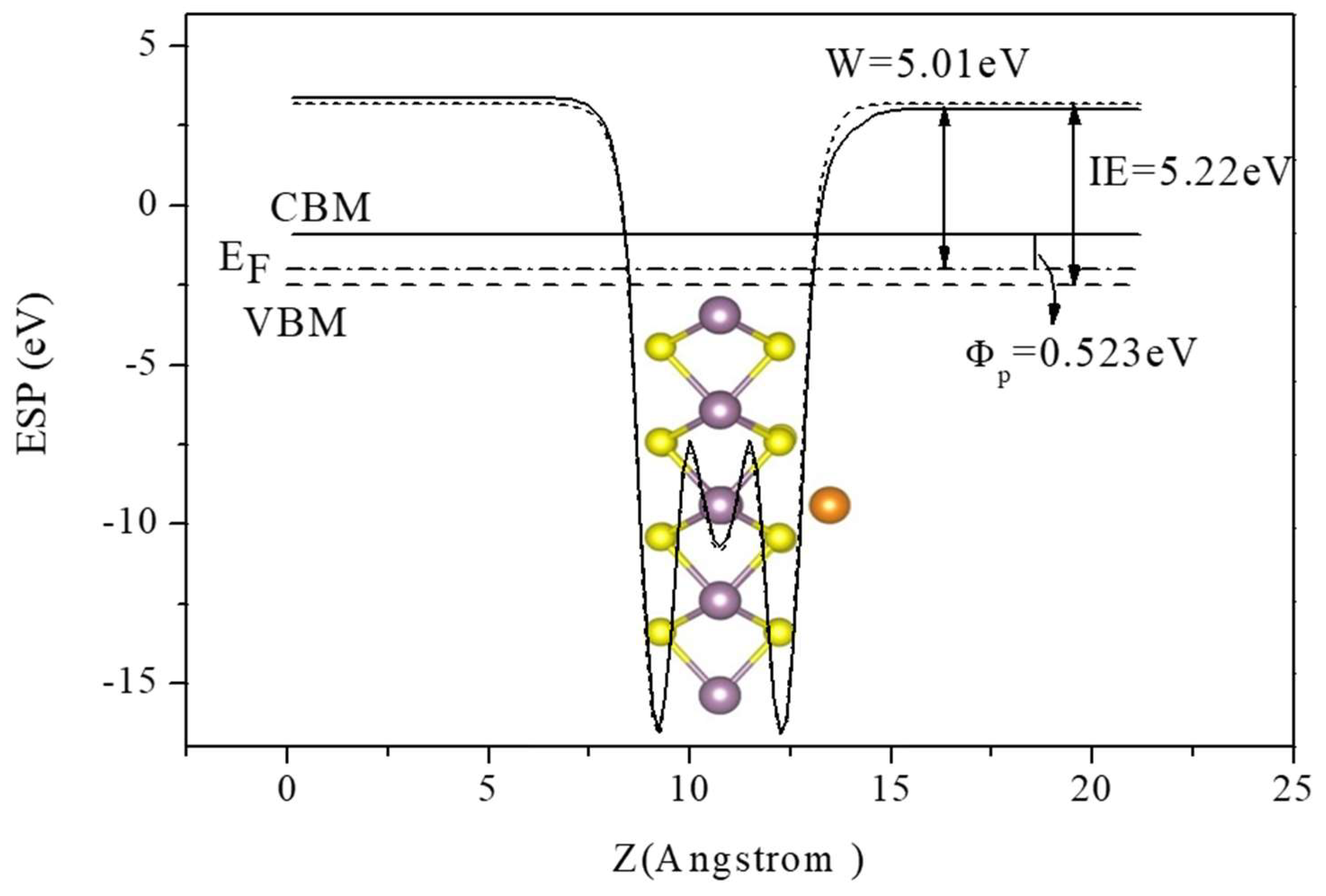
Figure 5 shows the in-plane averaged electrostatic potential (ESP) for the MoS2 surface with Pd monomer (solid line) and that of the pristine MoS2 surface (dotted line), respectively. The same were done for other Pd clusters, which are not shown here. Ionization energy (IE), defined as the energy difference between the vacuum level and valence band maximum (VBM), was determined to be 5.48 eV for the clean MoS2 ML. Upon the Pdn (n = 1–5) clusters adsorption, the increase of ionization energy (ΔI) was observed, which can be quantificationally given by the energy difference between the vacuum levels. In addition, the work function is described as the following equation: W = EvacEF, where Evac is the electrostatic potential in the vacuum region of the adsorbate side of the MoS2 surface, while EF refers to Fermi energy. The work function of pristine the MoS2 ML was estimated to be 5.26 eV, which is slightly higher than the experimental result of 5.03 eV [34].
As indicated in Figure 5, we also defined the energy difference between Fermi level (EF) and the CBM of the MoS2 ML as p-SBH (ΦP) for convenience, although the well-defined Schottky barrier contact had not formed yet in our considered initial growth stage of Pd clusters. In Table 4 we summarized the calculated work function (W), p-SBH (ΦP), dipole moments (Di), and the variation of ionization energy (ΔI) for the adsorption of Pd clusters. It became clear that the increasing of Pd coverage leads to decreases in the work function from 5.01 eV of Pd adatom to 4.38 eV of Pd5 cluster, which may result from the larger amount of CT from Pdn cluster to MoS2 as listed in Table 3. We think the variations of p-SBH are mainly attributed to the gap states caused by Pd adatoms (as shown in PDOS in Figure 3) and the partial charge transfer from 1stlayers to the second layer Pd atoms. The trend for the variations of ionization energy is obvious: as the cluster size increases (from Pd1 to Pd5), ΔI reduces rapidly, while ΔI rises in the initial growth stage of Ni clusters supported by MgO (001) [35]. In addition, the dipole moments (Di) were calculated by the product of transfer charge and the distance of adsorbate-substrate. The calculated dipole moments of Pdn/MoS2 were not in a monotonic variation, which is different from the monotonic increase of Di with the increase of Ni coverage on MgO (001).We think that the main reason for these distinct phenomena of the two systems is that the Pdn clusters injected electrons into the VBM of the MoS2 substrate while the Nin clusters extracted electrons from the MgO (001) surface. Besides, Pd adatom, Pd2, and Pd3 clusters prefer the planar structures as discussed above, and there is only the interface dipole contribution in such systems. For the cases of Pd4 and Pd5 clusters with pyramid-like structures, intra-cluster dipoles due to the CT between the topmost layer and the lower part of the cluster also contribute to the dipole moments. Since these two dipoles have opposite directions, the dipole interactions between Pd4 or Pd5 clusters and MoS2 substrate can be cancelled to some extent.
Previous studies have confirmed that the coverage-dependent depolarization effects play a non-negligible role in metal–organic interfaces [36,37,38]. In order to get insight into the coverage-dependent depolarization effects caused by the interaction between the adjacent supercells, we also used a (6 × 6) supercell to study the adsorption of Pdn clusters at the MoS2 substrate. We found that the CT and work function of Pdn (n = 1–3)/MoS2 systems have no significant change, while the variation on CT and work function for Pd4/MoS2 and Pd5/MoS2 were less than 0.04 and 0.01 eV, respectively. Therefore, the interactions between Pdn (n = 1–5) clusters within adjacent supercells is ignorable, and thus the coverage-dependent depolarization effects can be ignored in Pdn/MoS2 considered in this work. The discrepancy between metal–organic interfaces [36,37,38] and Pdn/MoS2 interface maybe explained by different interactions between adsorbates and substrate and different sizes of adsorbates, such as non-specific bonding between organic molecules and substrates versus the covalent Pd–S chemical bonds in our study, and larger diameters of organic molecules than that of metal clusters.

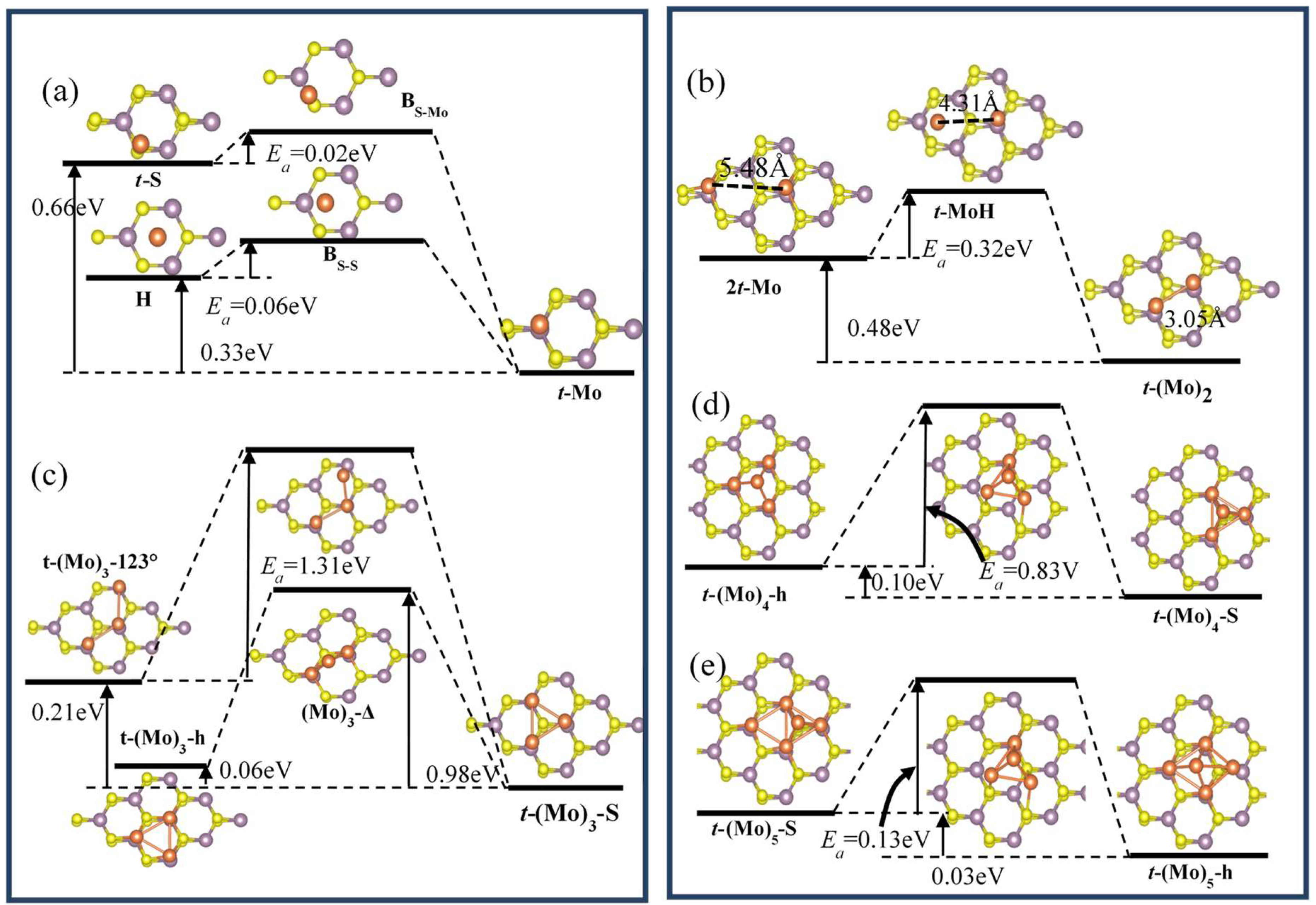
3.4. Diffusion of Pd Clusters on an MoS2 Monolayer

In order to investigate the nucleation mechanism and diffusion properties of Pd clusters on the MoS2 ML, we analyzed the diffusion and surface mobility of Pdn (n = 1–5) clusters on the MoS2 ML from the most favorable adsorption configurations. We defined the reaction rate k as the following:
k = v 0 exp ( Δ E a k B T ) ,  
where v 0 = 10 13 s 1 is the rate pre-factor, assumed to be irrelevant to the reaction or the hopping events, and kB and T are the Boltzmann constant and temperature, respectively. The equation indicated that reaction rate k is proportional to temperature T, while k is inversely related to the activation energy barrier Δ E a . In here, the activation energy barrier Δ E a is computed from the total energy difference between the initial configuration and the saddle points of the minimum energy pathway between two adsorption configurations. The k value is usually used to measure the possibility of nucleation and diffusion by overcoming the energy barrier at the low Pd coverage. The energy diagrams of Pdn (n = 1–5) clusters nucleated or diffused on the MoS2 ML are shown in Figure 6. As shown in Figure 6a, the calculated activation energies were 0.12 and 0.02 eV for the on-surface diffusion of Pd monomer along the two paths of t-S→t-Mo and H→t-Mo, respectively, which indicates the diffusion of Pd monomer on the MoS2 surface show remarkably anisotropy. The activation energy barrier was much smaller than the value of 0.34eV for Pd monomer diffusion on MgO (100) via single atom hops between oxygen sites [39], implying the Pd adatom on the MoS2 surface was mobile during the in situ growth by deposition. According to Equation (4), the number of hopping events per second between two TMo sites was estimated to be 103 s−1 along the Mo–H–Mo path and 10 s−1 along the Mo–S–Mo path at room temperature, respectively. The results indicated that the Pd adatoms are more likely to be mobile for coarsening and growth of large clusters rather than a random dispersion during the deposition. We also found that a newly deposited Pd atom prefers to bond to existing Pd adatoms located at t-Mo sites by possible diffusion, which is illustrated in Figure 6b. The energy barrier for the attachment of a Pd adatom to an existing Pd monomer to form Pd dimer is 0.32 eV, and the process is downhill by 0.48 eV. In other words, the deposited Pd adatoms are expected to bond to Pd monomer adsorbed at MoS2 rather than adsorb at a remote site. According to Equation (4), the higher the reaction temperature is, the easier the reaction occurs. For instance, the reaction rates k for the nucleation of Pd dimer from two Pd adatoms on MoS2 surface will increase about 140 and 485 times compared to that of room temperature (RT)under T = 500 and 600 K, respectively.
The three flat trimers t-(Mo)3-123°, t-(Mo)3-h, and t-(Mo)3-S shown in Figure 6b are easily accessible during metal deposition, which can be formed by the low-energy diffusion of Pd monomer on MoS2 surfaces to reach a Pd dimer. As shown in Figure 6b, although the total energies of the initial states of t-(Mo)3-123° and t-(Mo)3-h configurations were about 0.21 and 0.06 eV higher than that of the most stable configuration of t-(Mo)3-S due to the extra binding of the S1 atom, the energy barriers for transforming the flat t-(Mo)3-123° and t-(Mo)3-h configurations to t-(Mo)3-S were 1.31 and 0.92 eV, while the reverse processes were examined to surmount the energy barriers of 1.52 and 0.98 eV, respectively. We found that the transition state from t-(Mo)3-h to t-(Mo)3-S was Δ-(Mo)3, which was0.96 and 0.98 eV energetically higher than that of the initial and final states. However, the identical Δ-(Mo)3 configuration was predicted as the intermediate state with the lowest energy during the transformation between t-(Mo)3-h and t-(Mo)3-S configurations of Pt3 clusters on MoS2 ML as reported in Reference [14]. Such discrepancy may be due to the larger cohesive energy of Pt than that of Pd, which makes it is more likely to form islands for Pt NPs than Pd NPs.
We have considered various possible structures of palladium tetramer, which is formed by the simple extension from t-(Mo)3-S and t-(Mo)3-h via the attachment of Pd monomer to Pd3 clusters. The computed results show three-dimensional t-(Mo) 4-S was favored over t-(Mo) 4-h only by 0.10 eV in total energy, both of which can be nucleated on the MoS2 ML. It was clearly observed that transition from t-(Mo) 4-h to t-(Mo) 4-S should overcome the energy barrier of 0.83 eV, which is twice that of the transformation barrier of Pt4 clusters with the identical structures on the MoS2 ML [14]. It indicated that the diffusion of Pt4 clusters was likely to be much more accessible compared with Pd4 clusters on MoS2 MLs. Similarly, the most preferable configuration can be accessed from configurations t-(Mo4)-h and t-(Mo4)-S by deposition of new Pd atoms or diffusion of Pd monomers to the nearest-neighboring TMo site. The two pyramid-like Pd5 clusters labeled as t-(Mo)5-h and t-(Mo)5-S are shown in Figure 6e, respectively, which were found to be stable and have a slight energy difference of about 0.03 eV. The computed results show that the transformation of t-(Mo)5-h and t-(Mo)5-S was almost barrier less with Ea about 0.13 eV.
The diffusion of Pd atoms from the topmost site of a pyramid-like structure to the MoS2 substrate was a key factor to decide the growth mode of the Pdn cluster on the MoS2 monolayer. Therefore, we also calculated the diffusion behaviors of Pd atoms from topmost sites of Pd4 and Pd5 clusters to the MoS2 substrate. The calculated results show the topmost Pd atoms moving to the nearest-neighboring t-Mo sites of the MoS2 substrate needed to overcome the energy barriers of 0.73 and 1.13 eV for Pd4/MoS2 and Pd5/MoS2 systems, respectively. The relative high energy barriers imply that the Pd atoms prefer to form a sheet-supported metal nanotemplate on MoS2 in the initial growth stage, which is in conformity with the previous experimental study reported by Gong et al. [40] that Pd forms a uniform contact by physical vapor deposited on MoS2 monolayers.

4. Conclusions

In summary, we investigated theoretically the stable configurations, electronic structures, and surface mobility of Pdn (n = 1–5) clusters on MoS2 monolayers using first principles density functional theory calculations. The results demonstrate that Pd clusters can chemically adsorb on MoS2 MLs and Pd adatoms are strongly bound to the surface S atoms, which exhibit covalent bonds with significant ionic character. The geometries of Pdn cluster varies from a planar structure to a pyramidal morphology when the cluster size increases due to the relative strengths between Pdn–MoS2 and Pd–Pd interactions. Upon the deposition of Pd clusters, the band gaps of MoS2 weretunable due to the hybridization between 4d electrons of Pd and 3s electrons of S. The work function was modulated from 5.01 to 4.38 eV with the increase of Pd coverage, which resulted from the charge transfer from Pd clusters to MoS2 ML.
In addition, we investigated the nucleation and diffusion properties of Pdn (n = 1–5) clusters on MoS2 ML, e.g., the distant isolated Pd atoms or additional adatoms favor migrating to nearby Pdn clusters, which indicated that Pd is likely to agglomerate to metal nanotemplates on the MoS2 ML during the epitaxial stacking process. These findings may provide useful guidance to extend the potential technological applications of MoS2, including catalysts and production of metal thin films, and the fabrication of nanoelectronic devices.

Author Contributions

P.W. performed the calculation, data analysis, and wrote the manuscript; N.Y. and P.L. discussed the results and analyzed the data; and M.H. conceived the models and revised the manuscript.

Funding

This research was funded by the National Natural Science Foundation of China (Grant Nos. 11704237 and 11875183) and the High Education Key Program of Henan Province of China (No. 18A140027, 192102210205, and 192102210199).

Conflicts of Interest

The authors declare no conflict of interest.

References

  1. Xu, M.; Liang, T.; Shi, M.; Chen, H. Graphene-Like Two-Dimensional Materials. Chem. Rev. 2013, 113, 3766–3798. [Google Scholar] [CrossRef] [PubMed]
  2. Splendiani, A.; Sun, L.; Zhang, Y.; Li, T.; Kim, J.; Chim, C.Y.; Galli, G.; Wang, F. Emerging Photoluminescence in Monolayer MoS2. Nano Lett. 2010, 10, 1271–1275. [Google Scholar] [CrossRef]
  3. Chen, M.; Nam, H.; Wi, S.; Priessnitz, G.; Gunawan, I.M.; Liang, X. Multibit Data Storage States Formed in Plasma-Treated MoS2 Transistors. ACS Nano 2014, 8, 4023–4032. [Google Scholar] [CrossRef] [PubMed]
  4. Yu, Z.; Ong, Z.Y.; Li, S.; Xu, J.B.; Zhang, G.; Zhang, Y.W.; Shi, Y.; Wang, X. Analyzing the Carrier Mobility in Transition-Metal Dichalcogenide MoS2 Field-Effect Transistors. Adv. Funct. Mater. 2017, 27, 1604093. [Google Scholar] [CrossRef]
  5. Chen, S.; Wang, H.; Lu, S.; Xiang, Y. Monolayer MoS2 film supported metal electrocatalysts: A DFT study. RSC Adv. 2016, 6, 107836. [Google Scholar] [CrossRef]
  6. Fu, N.; Hu, Y.; Shi, S.; Ren, S.; Liu, W.; Su, S.; Zhao, B.; Weng, L.; Wang, L. Au nanoparticles on two-dimensional MoS2 nanosheets as the photoanode for efficient photoelectron chemical miRNA detection. Analyst 2018, 143, 1705–1712. [Google Scholar] [CrossRef] [PubMed]
  7. Burman, D.; Santra, S.; Pramanik, P.; Guha, P.K. Pt decorated MoS2 nanoflakes for ultrasensitive resistive humidity sensor. Nanotechnology 2018, 29, 115504. [Google Scholar] [CrossRef]
  8. Li, X.D.; Fang, Y.M.; Wu, S.Q.; Zhu, Z.Z. Adsorption of alkali, alkaline-earth, simple and 3d transition metal, and nonmetal atoms on monolayer MoS2. AIP ADV 2015, 5, 057143. [Google Scholar] [CrossRef]
  9. Shi, Y.; Huang, J.; Jin, L.; Hsu, Y.; Yu, S.F.; Li, L.J.; Yang, H.Y. Selective Decoration of Au Nanoparticles on Monolayer MoS2 Single Crystals. Sci. Rep. 2013, 3, 1839. [Google Scholar] [CrossRef]
  10. Guo, Y.; Dun, C.; Xu, J.; Li, P.; Huang, W.; Mu, J.; Hou, C.; Hewitt, C.A.; Zhang, Q.; Li, Y.; et al. Wearable Thermoelectric Device Based on Au Decorated Two-Dimensional MoS2. ACS Appl. Mater. Interfaces 2018, 10, 33316–33321. [Google Scholar] [CrossRef]
  11. Wang, X.; Tian, H.; Zhao, H.; Zhang, T.; Mao, W.; Qiao, Y.; Pang, Y.; Li, Y.; Yang, Y.; Ren, T. Interface Engineering with MoS2–Pd Nanoparticles Hybrid Structure for a Low Voltage Resistive Switching Memory. Small 2017, 14, 1702525. [Google Scholar] [CrossRef] [PubMed]
  12. Huang, X.; Zeng, Z.; Bao, S.; Wang, M.; Qi, X.; Fan, Z.; Zhang, H. Solution-phase epitaxial growth of noble metal nanostructures on dispersible single-layer molybdenum disulfide nanosheets. Nat. Commun. 2013, 4, 1444. [Google Scholar] [CrossRef] [PubMed]
  13. Song, B.; He, K.; Yuan, Y.; Sharifi-Asl, S.; Cheng, M.; Lu, J.; Saidi, W.A.; Yassar Reza, S. In Situ Study of Nucleation and Growth Dynamics of Au Nanoparticles on MoS2 Nanoflakes. Nanoscale 2018, 10, 15809. [Google Scholar] [CrossRef] [PubMed]
  14. Saidi, W.A. Density Functional Theory Study of Nucleation and Growth of Pt Nanoparticles on MoS2 (001) Surface. Cryst. Growth Des. 2015, 15, 642–652. [Google Scholar] [CrossRef]
  15. Jiang, C.; Wang, Y.; Zhang, Y.; Wang, H.; Chen, Q.; Wan, J. Robust Half-Metallic Magnetism in Two-Dimensional Fe/MoS2. J. Phys. Chem. C 2018, 122, 21617–21622. [Google Scholar] [CrossRef]
  16. Šljivančanin, Ž.; Belić, M. Graphene/MoS2 heterostructures as templates for growing two-dimensional metals: Predictions from ab initio calculations. Phys. Rev. Mater. 2017, 1, 044003. [Google Scholar] [CrossRef]
  17. Schulman, D.S.; Arnold, A.J.; Das, S. Contact engineering for 2D materials and devices. Chem. Soc. Rev. 2018, 47, 3037. [Google Scholar] [CrossRef] [PubMed]
  18. Fontana, M.; Deppe, T.; Boyd, A.K.; Rinzan, M.; Liu, A.Y.; Paranjape, M.; Barbara, P. Electron-hole transport and photovoltaic effect in gated MoS2 Schottky junctions. Sci. Rep. 2013, 3, 1634. [Google Scholar] [CrossRef] [PubMed]
  19. Dong, H.; Gong, C.; Addou, R.; McDonnell, S.; Azcatl, A.; Qin, X.; Wang, W.; Wang, W.; Hinkle, C.L.; Wallace, R.M. Schottky barrier height of Pd/MoS2 contact by large area photoemission spectroscopy. ACS Appl. Mater. Interfaces 2017, 9, 38977–38983. [Google Scholar] [CrossRef]
  20. Perdew, J.P.; Burke, K.; Ernzerhof, M. Efficient iterative schemes for ab initio total-energy calculations using a plane-wave basis set. Phys. Rev. Lett. 1996, 77, 3865–3868. [Google Scholar] [CrossRef]
  21. Kresse, G.; Furthmüller, J. Projector augmented-wave method. Phys. Rev. B Condens. Matter Mater. Phys. 1996, 54, 11169–11186. [Google Scholar] [CrossRef]
  22. Blochl, P.E. Projector augmented-wave method. Phys. Rev. B Condens. Matter 1994, 50, 17953. [Google Scholar] [CrossRef] [PubMed]
  23. Monkhorst, H.J.; Pack, J.D. Special points for Brillouin-zone integrations. Phys. Rev. B Solid State 1976, 13, 5188–5192. [Google Scholar] [CrossRef]
  24. Henkelman, G.; Uberuaga, B.P.; Jónsson, H. A climbing image nudged elastic band method for finding saddle points and minimum energy paths. J. Chem. Phys. 2000, 113, 9901. [Google Scholar] [CrossRef]
  25. Henkelman, G.; Jónsson, H. Improved tangent estimate in the nudged elastic band method for finding minimum energy paths and saddle points. J. Chem. Phys. 2000, 113, 9978. [Google Scholar] [CrossRef]
  26. Wu, P.; Yin, N.; Li, P.; Cheng, W.; Huang, M. The adsorption and diffusion behavior of noble metal adatoms (Pd, Pt, Cu, Ag and Au) on a MoS2 monolayer: A first-principles study. Phys. Chem. Chem. Phys. 2017, 19, 20713. [Google Scholar] [CrossRef] [PubMed]
  27. Li, H.; Huang, M.; Cao, G. Magnetic properties of atomic 3d transition-metal chains on S-vacancy-line templates of monolayer MoS2: Effects of substrate and strain. J. Mater. Chem. C 2017, 5, 4557–4564. [Google Scholar] [CrossRef]
  28. Matte, H.S.S.R.; Gomathi, A.; Manna, A.K.; Late, D.J.; Datta, R.; Pati, S.K.; Rao, C.N.R. MoS2 and WS2 Analogues of Graphene. Angew. Chem. Int. Ed. 2010, 49, 4059–4062. [Google Scholar] [CrossRef] [PubMed]
  29. Mak, K.F.; Lee, C.; Hone, J.; Shan, J.; Heinz, T.F. Atomically thin MoS2: A new direct-gap semiconductor. Phys. Rev. Lett. 2010, 105, 136805. [Google Scholar] [CrossRef] [PubMed]
  30. Saidi, W.A. Trends in the Adsorption and Growth Morphology of Metals on the MoS2(001) Surface. Cryst. Growth. Des. 2015, 15, 3190–3200. [Google Scholar] [CrossRef]
  31. Wang, Y.; Li, Y.; Chen, Z. Not your familiar two-dimensional transition metal disulfide: Structural and electronic properties of the PdS2 monolayer. J. Mater. Chem. C 2015, 3, 9603. [Google Scholar] [CrossRef]
  32. Wu, P.; Cao, G.; Tang, F.; Huang, M. First-principles study of small palladium clusters on NiAl(110) alloy surface. Physica E 2013, 53, 7–13. [Google Scholar] [CrossRef]
  33. Wang, B.; Yoon, B.; König, M.; Fukamori, Y.; Esch, F.; Heiz, U.; Landman, U. Size-Selected Monodisperse Nanoclusters on Supported Graphene: Bonding, Isomerism, and Mobility. Nano Lett. 2012, 12, 5907–5912. [Google Scholar] [CrossRef] [PubMed]
  34. Kwon, S.; Choi, S.H.; Kim, Y.J.; Yoon, I.T.; Yang, W. Proton beam flux dependent work function of mono-layer MoS2. Thin Solid Films 2018, 660, 766–770. [Google Scholar] [CrossRef]
  35. Dong, Y.F.; Wang, S.J.; Mi, Y.Y.; Feng, Y.F.; Huan, A.C.H. First-principles studies on initial growth of Ni on MgO(001) surface. Surf. Sci. 2006, 600, 2154–2162. [Google Scholar] [CrossRef]
  36. Topham, B.J.; Kumar, M.; Soos, Z.G. Profiles of Work Function Shifts and Collective Charge Transfer in Submonolayer Metal–Organic Films. Funct. Mater. 2011, 21, 1931–1940. [Google Scholar] [CrossRef]
  37. Monti, O.L.A. Understanding Interfacial Electronic Structure and Charge Transfer: An Electrostatic Perspective. J. Phys. Chem. Lett. 2012, 3, 2342–2351. [Google Scholar] [CrossRef]
  38. Piacenza, M.; D’Agostino, S.; Fabiano, E.; Sala, F.D. Ab initio depolarization in self-assembled molecular monolayers: Beyond conventional density-functional theory. Phys. Rev. B 2009, 80, 153101. [Google Scholar] [CrossRef]
  39. Xu, L.; Henkelman, G.; Campbell, C.T.; Jónsson, H. Small Pd Clusters, up to the Tetramer At Least, Are Highly Mobile on the MgO(100) Surface. Phys. Rev. Lett. 2005, 95, 146103. [Google Scholar] [CrossRef]
  40. Gong, C.; Huang, C.; Miller, J.; Cheng, L.; Hao, Y.; Cobden, D.; Kim, J.; Ruoff, R.S.; Wallace, R.M.; Cho, K.; et al. Metal Contacts on Physical Vapor Deposited Monolayer MoS2. ACS Nano 2013, 7, 11350–11357. [Google Scholar] [CrossRef]
Figure 1. (a) Top and side views for the pristine MoS2 monolayer (ML); S and Mo atoms are in yellow (small) and lavender (large) spheres, respectively. (b) Band structure of pristine MoS2 monolayer and Fermi level is indicated by gray dashed line.
Nanomaterials 09 00395 g001
Figure 2. (ad) Top and side views for most stable configurations of palladium dimer, trimer, tetramer, and pentamer adsorbed at the MoS2 monolayer, respectively. The yellow, lavender, and orange balls represent S, Mo, and Pd atoms, respectively.
Nanomaterials 09 00395 g002
Figure 3. (a) Partial density of states (PDOS) of isolated Pd atoms and S and Mo of pristineMoS2 ML. (bf) PDOS of Pd adatoms of Pdn (n = 2–5) clusters and surrounding S and Mo of underlying MoS2 substrate. The Fermi level was set to 0 eV and is represented by the dashed lines.
Nanomaterials 09 00395 g003
Figure 4. (ae) Charge density difference plots for the most stable configurations Pdn (n = 1–5) clusters adsorbed on the MoS2 monolayer. Top and bottom images show the top and side views of adsorption configurations, respectively. Yellow regions represent charge accumulation, and blue regions show charge loss. The iso-surface value was0.001 e Å−3.
Nanomaterials 09 00395 g004
Figure 5. In-plane averaged electrostatic potential (ESP) for the MoS2 surface adsorbed with isolated Pd atom (solid line) and pristine MoS2 (dotted line). The values of work function (W), ionization energy (IE) for the MoS2 surface, and p-SBH (ΦP) are indicated.
Nanomaterials 09 00395 g005
Figure 6. (ae) Energy diagrams for the transformation between considered configurations of Pdn (n = 1–5) clusters on MoS2 surfaces. (a) The diffusion of a Pd adatoms from t-S and H sites to the most favorable t-Mo site, and (b) the nucleation process of Pd dimer on MoS2 surface. (ce) The transformation to the most stable energy configurations of Pdn (n = 3–5) clusters on MoS2 surfaces.
Nanomaterials 09 00395 g006
Table 1. The structural parameters (Å) and calculated adsorption energies EA (eV) for Pd monomer adsorbed at four high-symmetry sites of MoS2 monolayer.
SitedPd–ModPd–SdMo–ShPd-subEA
t-Mo2.832.342.401.332.16
H3.642.422.431.591.79
t-S4.182.182.432.191.59
BS-S
Table 2. Calculated distance between Pd clusters and MoS2 surface (dPd-substrate), bond length of Pd–S (dPd–S), Pd–Pd distance (dPd–Pd), adsorption energy EA, binding energy EB, and intra-cluster binding energy EIB for the lowest energy Pdn (n =1–5) configurations on the MoS2 ML. The units of structural parameters and energies are Å and eV, respectively.
ConfigurationsPdPd2Pd3Pd4Pd5
t-Mot-(Mo)2t-(Mo)3-St-(Mo)4-St-(Mo)5-h
dPd-substrate1.331.421.491.461.44
dPd-S2.342.31, 2.35, 2.422.28, 2.462.43, 3.492.33, 2.42, 2.47, 2.51
dPd-Pd3.052.942.67, 3.022.63, 2.74, 3.05, 3.20
EA2.161.841.440.930.86
EB2.212.292.362.38
EIB0.370.851.431.52
Table 3. Bader charge analysis for the lowest energy configurations of Pdn (n = 1–5) clusters supported by the MoS2 ML.
ConfigurationsPd1Pd2Pd3Pd4Pd5
first layer9.749.80(2)9.82(3)9.80(2), 9.829.78(2), 9.79, 9.89
second layer10.1410.15
Bader charge0.260.400.540.440.61
Table 4. Calculated work function (W), p-SBH (ΦP), dipole moment (Di), and variations of ionization energy (ΔI) upon the adsorption of the lowest energy Pdn (n = 1–5) clusters on the MoS2 ML.
ConfigurationsPd1Pd2Pd3Pd4Pd5
W (eV)5.014.734.624.464.38
ΦP (eV)0.520.821.001.181.27
ΔI (eV)0.170.160.080.060.05
Di (eÅ−1)0.350.570.800.640.88

