Abstract
Flexible electronic systems have received increasing attention in the past few decades because of their wide-ranging applications that include the flexible display, eyelike digital camera, skin electronics, and intelligent surgical gloves, among many other health monitoring devices. As one of the most widely used technologies to integrate rigid functional devices with elastomeric substrates for the manufacturing of flexible electronic devices, transfer printing technology has been extensively studied. Though primarily relying on reversible interfacial adhesion, a variety of advanced transfer printing methods have been proposed and demonstrated. In this review, we first summarize the characteristics of a few representative methods of transfer printing. Next, we will introduce successful demonstrations of each method in flexible electronic devices. Moreover, the potential challenges and future development opportunities for transfer printing will then be briefly discussed.
1. Introduction
The increasing popularity of intelligent terminals has driven the rapid development of bio-integrated and implantable electronic devices. These classes of emerging high-performance electronics are lightweight, flexible, and highly sensitive, which opens application opportunities in skin-like electronics, wearable health monitoring devices, and human-machine interfaces. A few representative examples used in biomedical diagnostics include flexible digital x-ray detectors, medical balloon catheters, bio-integrated neural electrode arrays, and soft surgical gloves. Because of the intrinsically flexible and stretchable properties, low-cost fabrication processes, and compatibility with the solution process, the use of organic materials for flexible and stretchable electronics is straightforward [1,2,3,4,5]. However, compromised electrical properties limit their use in certain applications where high performance is desirable [5,6,7]. As an alternative to intrinsically stretchable organic materials, inorganic semiconducting and conducting materials designed in a stretchable layout exhibit outstanding electrical properties, such as high conductivity and charge carrier mobility, yielding devices with performances comparable to those fabricated with conventional wafer-based technologies [6,7,8].
As the high-performance of a device hinges on its fabrication process, it is highly desirable to fabricate stretchable inorganic devices on the conventional substrate with the photolithographic or other similar processes [9,10,11]. To provide a robust handling substrate, and also an interface to the soft tissues, the fabricated inorganic devices would need to be integrated onto the flexible and stretchable substrates [12,13,14,15,16,17,18]. The process to transfer the devices fabricated from the growth (donor) substrate to the receiving substrate can be achieved via a stamp by a technique termed as transfer printing [19,20,21,22,23,24].
As one of the most widely used methods for the fabrication of flexible and stretchable inorganic photonic/electronic devices, transfer printing [22,25,26,27,28,29] provides a versatile route to deterministically assemble micro- and nano-materials into spatially organized, functional arrangements with two- and three-dimensional layouts [30,31,32]. The transfer printing method is also suitable for large-scale assembly [7,19,33,34,35,36,37,38,39]. The typical transfer printing process consists of two steps: Pickup and printing (Figure 1). In the pickup step, functional device components (e.g., micro-/nano-membranes, ribbons, nanowires, nanotube, etc.) pre-fabricated on the donor substrate are first picked up onto a stamp. In the printing step, the inked stamp is then brought into contact with the receiver, followed by the removal of the stamp to print the device components onto the receiving substrate (receiver). The stamp used in both the pickup and printing steps is clearly the key to the successful implementation of the transfer printing process with a high fidelity and easy control [25,40,41].
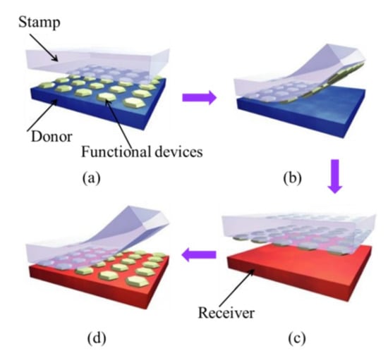
Figure 1.
Schematic illustration of the transfer printing process: (a) Laminating the stamp against the donor substrate, on which the functional devices are fabricated; (b) peeling the stamp to transfer the functional devices from the donor substrate onto the stamp; (c) bringing the inked stamp into contact with the receiving substrate (receiver); (d) peeling the stamp to print the functional devices onto the receiver. Reprinted with permission from [24]; Copyright 2006, Nature Publishing Group.
The transfer printing process involves the competing fracture at the stamp/device interface and the device/substrate (donor or receiver) interface. The fracture at the stamp/device interface occurs in the printing step, whereas the fracture at the device/donor interface occurs in the pickup step [24,25,42]. The successful pickup requires the adhesion strength at the stamp/device interface to be larger than that at the device/donor interface, resulting in delamination at the device/donor interface to transfer the functional devices onto the elastomeric stamp (Figure 2a). Conversely, the adhesion strength at the device/receiver interface is stronger than that at the stamp/device interface in the printing step. Consequently, peeling off the stamp prints the functional devices onto the receiver (Figure 2b).
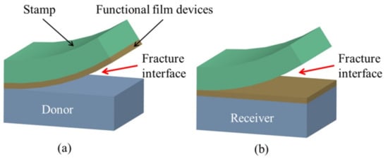
Figure 2.
The diagram to show the (a) pickup and (b) printing steps in the transfer printing process. In the pickup step, the crack propagates at the device/donor interface, whereas delamination occurs at the device/stamp interface in the printing step. Reproduced with permission from [25]; Copyright 2007, American Chemical Society.
As the successful transfer printing process hinges on the modulation of the interfacial adhesion at different material/structural interfaces [40], efforts have been dedicated to the exploration of feasible methods for the modulation of interfacial adhesion strength. Among the various techniques being developed, the straightforward ones include kinetic adhesion control [24,25,43,44], modification of the surface chemistry [45,46], and solvent-assisted adhesion control [47,48]. Though effective, these methods typically involve the use of the solvent or etchant to remove sacrificial layers, which would cause irreversible damage to the various functional components in the device system and compromise the device performance. As a result, the techniques that are based on mechanical principles for reversible adhesion modulation have started to gain momentum.
Transfer printing technology is associated with several salient advantages: (1) The device components fabricated with the conventional wafer-based technologies enable high performance of the electronic systems; (2) the deterministic assembly is efficient, with high precision; (3) the transfer printing process is repeatable even at large-scale integration, such as the roll-to-roll application for both 2D and 3D layouts [49]; (4) certain transfer printing techniques can be operated at room temperature with low cost; and (5) it is applicable to a wide range of structures and materials, ranging from the assembly of micro-/nano-structures in various shapes and sizes to materials that include organic molecular materials [50,51]; inorganic semiconducting materials, such as GaAs/GaN/etc. [52]; functional polymers [53]; metals; piezoelectric materials; and many others.
Given the existing reviews on the technique of transfer printing that mainly focus on the mechanics, materials, and applications [30,54,55,56], this review will summarize the recent developments of transfer printing techniques in Section 2 and their applications in the fabrication process for various flexible and stretchable electronic devices in Section 3. The challenges and future directions of transfer printing will then be discussed in Section 4.
2. Transfer Printing Methods
To explore the full potential of different transfer printing techniques, it is important to understand the underlying mechanisms of different techniques, as well as the advantages and limitations of each transfer printing method.
2.1. Kinetically Controlled Transfer Printing
Based on the kinetically dependent nature of the viscoelastic stamp [24,25,44], the adhesion strength between the stamp and the functional devices can be modulated by the retraction speed of the stamp. Without using the adhesive layer, van der Waals forces are sufficient in this mode of operation. While the substrate and functional device components (modeled as thin films) are elastic, the critical energy release rate at the film/substrate interface, , remains unchanged during the transfer printing process. However, with the use of the viscoelastic stamp, the critical energy release rate at the stamp/film interface, , is rate-sensitive and depends on the peeling velocity. A viscoelastic model, validated by the numerical and experimental results, describes this rate-dependent behavior and the result shows that the pull-off force increases with the peeling velocity [57]. The critical energy release rate, , that monotonically increases with the peeling velocity, v, (Figure 3) can be expressed as:
where is the critical energy release rate when the peeling velocity approaches zero, is the reference peeling velocity at which the critical energy release rate equals to , and the exponent, n, is a scaling parameter that can be obtained by the experiment.
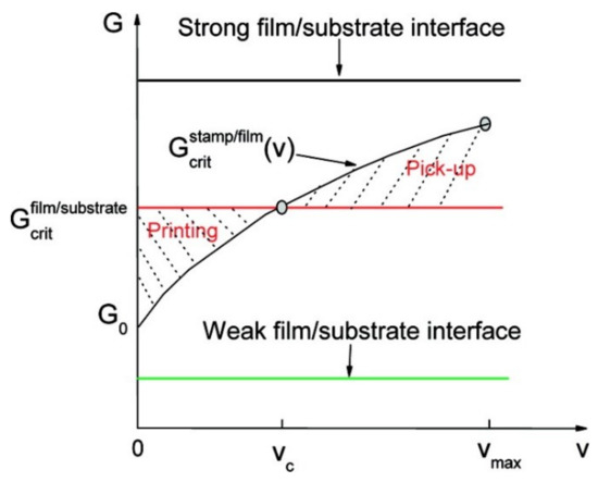
Figure 3.
Schematic diagram of critical energy release rates at the film/substrate and film/stamp interfaces as a function of the peeling velocity. In the pickup step, the critical energy release rate at the film/stamp interface is larger than that at the film/substrate interface, leading to the crack propagation at the film/substrate interface and a retrieval of the device film from the donor substrate onto the stamp. In the printing step, the critical energy release rate at the film/stamp interface is smaller than the critical energy release rate at the film/receiver interface, which allows the crack propagation at the film/stamp interface and helps release the device film onto the receiver substrate. Reproduced with permission from [25]; Copyright 2007, American Chemical Society.
By adjusting the peeling velocity applied on the viscoelastic stamp, the adhesion at the device/stamp interface can be easily modulated to yield controlled delamination: A sufficiently high velocity for pickup (Figure 2a) and then a slow retraction for printing (Figure 2b). Though this kinetically controlled transfer printing technique provides a pragmatic, easy-to-operate tactic to assemble functional devices onto various flexible substrates, the range of modulation is limited due to the restriction of the peeling speed. Moreover, this method is not applicable when the receiver is also viscoelastic, limiting its application to certain classes of materials as the receiver.
2.2. Thermal Release Transfer Printing
As one of the most widely used methods, transfer printing based on the use of a thin and flexible thermal release tape (TRT) is simple to operate and a fracture mechanics model is used in the analysis [58]. The technique relies on the large and irreversible reduction in the adhesion strength when the TRT is heated over the transition temperature (i.e., 100 °C) (Figure 4). The quantitative dependence of the energy release rate at the functional membrane/TRT interface is characterized by Equation (2), which is a function of the temperature and peeling velocity. With the additional control in the temperature, the ratio of strong to weak adhesion becomes larger when compared to the technique that only uses the kinetic control:
where is the temperature, is the Euler’s constant, is the critical energy release rate when the adhesives on TRT are deactivated, is the transition temperature, is a material parameter, and the other parameters are the same as in Equation (1).
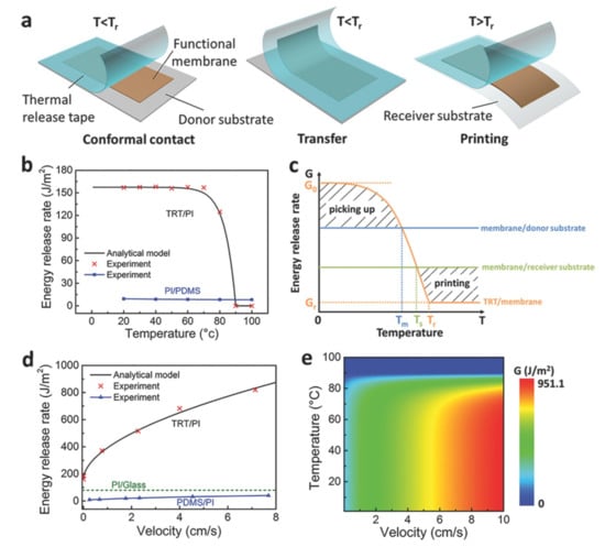
Figure 4.
(a) Schematic illustration of transfer printing that uses a thermal release tape. The energy release rate at the TRT/Polyimide (PI) and PI/Polydimethylsiloxane (PDMS) interfaces as a function of (b) the temperature and (d) peeling velocity. (c) The modulation of the energy release rate via temperature is used for the pickup and printing steps. (e) A contour map shows the energy release rate at the TRT/PI interface as a function of the temperature and peeling velocity. Reproduced with permission from [58]; Copyright 2017, WILEY-VCH Verlag GmbH & Co., KGaA, Weinheim.
The modulation of the critical energy release rate at the TRT/membrane interface is mainly controlled by the peeling velocity and temperature as described in Equation (2). The critical energy release rate, , remains almost unchanged for temperatures below 70 °C (Figure 4b), which is much larger than the critical energy release rate at the membrane/donor interface, . Because the crack propagation occurs at the device/substrate interface, the membrane devices could be easily picked up. When the TRT/membrane system is heated above 80 °C, the critical energy release rate, , significantly decreases to be smaller than the critical energy release rate at the membrane/receiver interface, . Upon peeling off the TRT, the crack propagates at the TRT/membrane interface, which facilitates the printing of the membrane devices onto the receiver substrate. As the critical energy release rate, , can be modulated with the peeling velocity and temperature over a large range (Figure 4d,e), the thermal release transfer printing represents a powerful method in the device integration.
2.3. Water-Assisted Transfer Printing
With the use of a thin Ni layer between the device and the donor (e.g., Si wafer coated with SiO2), the water-assisted transfer printing method (WTP) is developed to integrate electronic devices, such as those based on nanowires (NW) on different substrates (Figure 5) [59,60,61]. Peeling-off in a water bath at room temperature transfers the device and the Ni layer onto the thermal release tape. Following the Ni etching and a printing step delivers the device to different non-conventional substrates without defects.
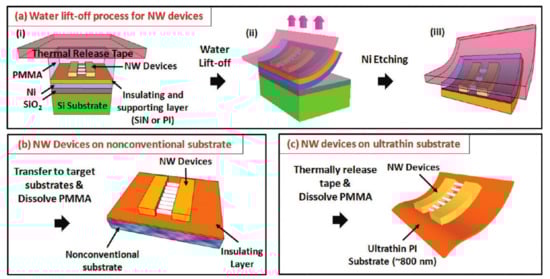
Figure 5.
Schematic illustration of water-assisted transfer printing. (a) After depositing a thin Ni layer on the Si wafer coated with SiO2, the nanowire (NW) devices are fabricated on an insulating and supporting layer (SiN or PI). Lift-off in a water bath at room temperature allows the transfer of the nanowire device and the Ni layer onto the thermal release tape. A subsequent Ni etching removes the Ni layer. The devices with an insulating layer can then be printed onto (b) a nonconventional substrate or (c) an ultrathin polyimide substrate. Reproduced with permission from [59]; Copyright 2011, ACS publications.
The successful operation of WTP clearly depends on the water-assisted interfacial fracture at the Ni/SiO2 interface. Deposition of the Ni layer on the Si wafer coated with SiO2 forms nickel silicate or nickel oxide, which results in Ni hydroxide when it is immersed in the water. As both the SiO2 and Ni hydroxide are hydrophilic, water can quickly penetrate at the interface to result in interface separation. Because the lift-off is operated at room temperature, the possible damage from high temperatures can be avoided. The detailed working principle of the interfacial debonding process is studied through theory, experiment, and finite element analysis [62].
In a different approach, a water-mediated transfer printing method is developed to print Al thin films on a substrate as shown in Figure 6a [63] and Figure 6b [64]. Although there are some slight differences between the two transfer printing processes, their working principle is the same. That is, the self-assembled monolayers (SAM) layer weakens the adhesion strength between the Al thin film and the stamp/glass inkpad in the pickup step and enables the facile and complete release of the Al thin film. The water layer on the substrate, as the most critical part, serves as an adhesion layer, promoting the adhesive bonding between the Al thin film and the target substrate. For example, as shown in Figure 6b, spontaneously formed on the donor glass substrate, a thin organic self-assembled monolayer (SAM), such as octadecylsiloxane, facilitates the release of Al onto the PDMS stamp in the pickup step. In the printing step, the water layer pre-formed on the receiver surface promotes the interface adhesion at the Al/receiver interface.
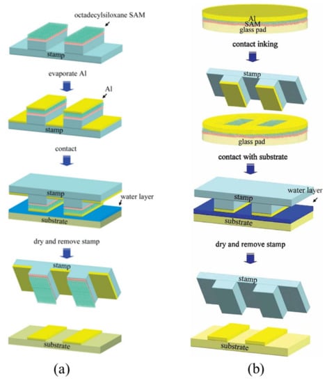
Figure 6.
Schematic illustration of the water-mediated transfer printing process: (a) Firstly, the patterned PDMS stamp coated by SAM is fabricated. Secondly, the Al thin film is evaporated onto the SAE layer. Then, the inked stamp is brought to contact with the target substrate covered by a thin water layer. Finally, peeling off the stamp from the substrate after drying completes the print process. (Reproduced with permission from [63]; Copyright 2007, WILEY-VCH Verlag GmbH & Co., KGaA, Weinheim). (b) The Al thin film is first deposited onto the SAM-coated glass pad (donor substrate), where the SAM layer facilitates the release of the Al thin film onto the PDMS stamp. Then, the inked stamp is brought into contact with the substrate coated with a water layer to enhance the adhesion strength between the Al thin film and the receiver. Finally, the stamp is removed to print the Al film on the receiver upon the drying of the water (Reproduced with permission from [64]; Copyright 2009, WILEY-VCH Verlag GmbH & Co., KGaA, Weinheim).
2.4. Surface Relief Structure-Assisted Transfer Printing
The interfacial adhesion strength dominated by van der Waals interaction is directly related to the contact area at the interface. Leveraging the idea of structural collapse [65,66], a surface relief structure-assisted transfer printing method was developed to mimic the reversible dry adhesion at the gecko’s foot [67]. Instead of using stamps with a flat surface, the soft stamp is designed with pyramidal microtips on its surface (Figure 7). In the pickup step, the applied pressure collapses the pyramidal microtips to increase the contact area, thereby enhancing the adhesion at the stamp/device interface for pickup. After placing the inked stamp onto the receiver, the removal of the pressure leads to the recovery of the pyramidal microtips for a significantly reduced contact area, minimizing the adhesion strength at the stamp/device interface for printing (Figure 7e). It should be noted that it is also possible to combine the principle of kinetically dependent adhesion by a rapid peeling in the pickup (Figure 7c) and/or a slow retraction in the printing (Figure 7f) to further increase the range of modulation in the interfacial adhesion strength.
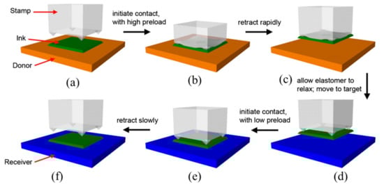
Figure 7.
Schematic of surface relief structure-assisted transfer printing. (a) A stamp with four pyramidal microtips at each corner is first brought into contact with the functional device components, followed by (b) an external pressure to result in the collapse of the microtips. (c) Rapid retraction of the stamp transfers the device component onto the stamp. (d) The inked stamp is then transported to the receiver. (e) Without the pressure, the microtips on the stamp recover to minimize the contact area at the stamp/device interface. (f) A slow retraction then prints the device component onto the receiver. Reproduced with permission from [67]; Copyright 2010, National Academy of Sciences of the United State of America.
As it is desirable to have a reversible adhesion, it is critical to design the geometry of the microtips, such as its height. Two- and three-dimensional mechanics models are established [68] to determine the range of heights. The expressions of the minimum and maximum heights of the microtips are deduced in the two- and three-dimensional models to investigate the influence of the height of the microtips on the reversible adhesion strength. Verified by the experiments, the analytical study provides useful guidelines in the design of surface structures.
Similar to the idea of changing the contact area at the stamp/device interface, a variety of viscoelastic stamps with different surface relief structures have been designed, including patterned pillars [69], grating-like reliefs [70,71], angled micro-flaps [72], and many others (Figure 8).
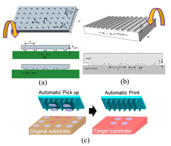
Figure 8.
Various viscoelastic stamps with different surface relief structures: (a) Micro-pillars (Reproduced with permission from [69]; Copyright 2013, Elsevier), (b) grating-like reliefs (Reproduced with permission from [70]; Copyright 2013, AIP Publishing LLC), and (c) angled micro-flaps (Reproduced with permission from [72]; Copyright 2014, American Chemical Society).
2.5. Shear-Assisted Transfer Printing
With the same inspiration from the gecko’s foot, the directionally dependent dry adhesion has also been applied to transfer printing, resulting in the shear-assisted technique [73,74]. The analytical model [75], validated by the experiment, indicates that a shear displacement on the stamp greatly reduces the critical energy release rate at the device/stamp interface, which helps the separation at the interface. The pull-off force needed for delamination at the device/stamp interface decreases almost linearly with the increasing shear strain. In view of this, the shear displacement is applied in the printing step (Figure 9).
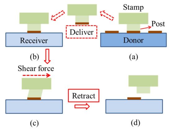
Figure 9.
Schematic illustration of shear-assisted transfer printing. (a) The stamp is retracted rapidly from the donor substrate to pick up the device component. (b) After bringing the inked stamp into contact with the receiver, (c) a shear force is applied to reduce the pull-off force at the device/stamp interface. (d) A slow retraction then prints the device component onto the receiver. Reproduced with permission from [75]; Copyright 2012; Elsevier.
2.6. Transfer Printing Based on Shape Memory Polymer
Capable of switching between temporary and permanent shapes, shape memory polymer (SMP) provides an alternative material to the conventional PDMS stamps in transfer printing. SMP can memorize the temporary shape formed by various pre-loads and easily recover its permanent shape after being triggered by an external stimulus (e.g., heat, electricity, light, moisture, etc.) [76,77,78,79]. In a representative use, the SMP stamp with a permanent shape of the relief structure, such as the example discussed in Figure 7, can be programmed to have a temporary shape of the collapsed state (Figure 10) [80,81]. The temporary shape with a large contact area and high interfacial adhesion strength is used in the pickup step. Upon heating, the SMP stamp recovers to its permanent shape with a significantly reduced contact area and low interfacial adhesion strength, which is then used for printing. Such temperature controlled transfer printing with the use of the SMP stamp is studied by an analytical model and the results provide optimized surface relief structures [82]. Though effective and easy to operate, the use of the SMP stamp may involve high temperatures, resulting in damage to delicate functional micro-devices and substrates. Moreover, it is not easy to apply in industrial-scale manufacturing.
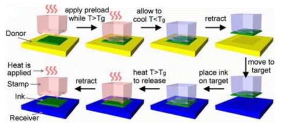
Figure 10.
Schematic illustration for the transfer printing method based on shape memory polymers. When the temperature is heated above the transition temperature, applying a preload leads to collapse at the microtips and increases the contact area between the stamp and the donor to yield an increased adhesion at the ink/donor interface. Cooling down the temperature to a value below the transition temperature, the shape memory polymer stamp is programmed to this temporary shape for the transferring of the ink in contact. After bringing the inked stamp into contact with the receiver, heating above the transition temperature allows the SMP stamp to recover its permanent shape with a significantly reduced contact area for a much lower interfacial adhesion strength to release the ink onto the receiver. Reproduced with permission from [80]; Copyright 2014, IEEE.
2.7. Laser-Assisted Transfer Printing
Building on the idea of the thermal mismatch from the thermo-mechanical response of multilayered structures with different materials, a laser pulse is introduced in the printing step to initiate the separation of the device components from the stamp, where the device component does not need to be in contact with the receiver (Figure 11) [83,84]. The success of the non-contact laser-assisted transfer printing method closely depends on the laser pulse used in the printing step.
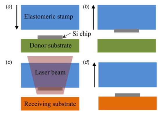
Figure 11.
Schematic illustration of laser-assisted transfer printing. (a) Aligning the stamp with the donor substrate and (b) applying a rapid retraction on the stamp picks up the Si chip. (c) Applying a laser pulse initiates the separation at the device/stamp interface to (d) deliver the Si chip onto the surface of the receiver. Reproduced with permission from [88]; Copyright 2017, ASME.
By avoiding direct contact between the functional device components and the target substrate, laser-assisted transfer printing expands the range of the receiving substrate (with different geometrical and material properties) in the integration process. To analyze the mechanism of delamination induced by the laser pulse, analytical mechanics models, validated by experiments and the finite element analysis, are also established to relate the energy release rate with the temperature distribution resulting from the laser pulse [33,85,86,87] and the influence of the device size on the temperature distribution is specifically analyzed [88]. Though it offers the versatility to print functional device components onto various flat, curved, or even partially defected substrate surfaces, laser-assisted transfer printing would require a relatively precise control of the intensity and irradiation time of the laser pulse, which is typically associated with expensive equipment.
2.8. Intaglio Transfer Printing Method
Choi et al. [89] developed an intaglio transfer printing method for creating quantum dot (QD) arrays, which is slightly different from conventional methods. This method enabled the nanocrystal layers to be transfer-printed on various substrates without consideration of the size and shape. The whole transfer printing process is shown in Figure 12, in which the QD layer is firstly pre-fabricated on a Si source substrate. The flat PDMS stamp is in good contact with the QD layer to pick it up quickly. Then, the inked stamp is moved to contact on the intaglio trenches carved on the Si substrate (it is the special feature of this method) and is pressed with low pressure. In the third step, peeling off the stamp slowly makes the intaglio QD patterns form on the PDMS stamp rather than on the Si substrate, and the rest of the QD layer is released on the Si substrate. Finally, the inked stamp is transferred to print the QD layer onto the target substrate. Ultimate QD arrays can be completed through repetitive aligned transfer printing. It is worth mentioning that the current method can be generalized to transfer various QD layers regardless of the QD materials. Furthermore, the intaglio trenches are reusable because the residual QD layers on the trench can be eliminated easily through either mechanical rubbing or cleaning in a piranha solution.
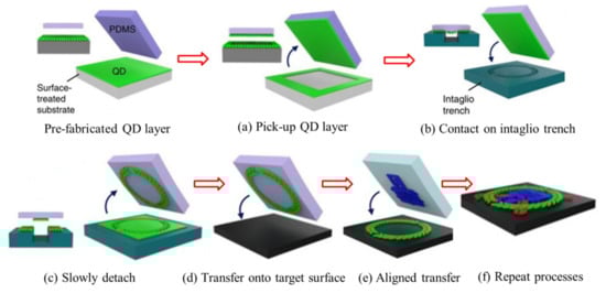
Figure 12.
Schematic illustration of the transfer printing process of the pre-fabricated quantum dot (QD) layer: (a) The pre-fabricated QD layer is picked up quickly by the PDMS stamp; (b,c) the inked stamp is moved to contact on the intaglio trench and detached slowly to form QD patterns on the PDMS stamp; (d,e) the formed QD patterns are transfer printed on the target substrate; (f) QD arrays fabricated through repeat transfer printing processes. Reproduced with permission from [89]; Copyright 2015, Macmillan Publishers Limited.
2.9. Magnetic-Assisted Transfer Printing
As an alternative approach to trigger the transfer printing by an external field, magnetic-assisted transfer printing was developed with the use of a magnetic-responsive film [90,91] or magnetic particles [92] to deform the elastic film. The former exploits a structurally designed stamp with an incompressible liquid chamber stacked on top of a gas chamber. The liquid chamber uses a magnetic-responsive thin film and a PDMS thin film at the top and bottom surface, respectively. In the pickup (printing) step, the top magnetic-responsive thin film is actuated by the external magnetic field to deform upward (downward), which transfers the motion to the bottom PDMS film and then induces a decreased (increased) pressure in the gas chamber (Figure 13). The pressure change in the gas chamber modulates the interfacial adhesion. The pressure change in the gas chamber as a function of the displacement profile of the top magnetic-responsive film is established in the analytical model, providing a comprehensive design guideline for the magnetic-assisted transfer printing.
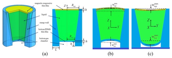
Figure 13.
Schematic illustration of a structurally designed stamp consisting of an incompressible liquid chamber on top of a gas chamber in magnetic-assisted transfer printing. (a) 3D representation and cross-sectional views of the stamp design, with cross-sectional views of the stamp deformed upon the external magnetic actuation in the (b) pickup and (c) printing step. Reproduced with permission from [91]; Copyright 2018, ASME.
With the above description of the various transfer printing methods, it can be safely concluded that each transfer method is associated with different characteristics for integration of the functional thin film devices on a compliant substrate. To help highlight the differences among the different transfer printing methods, we summarized the working principles, advantages, and limitations for each transfer printing method in Table 1.

Table 1.
Comparison of various transfer printing methods.
3. Development and Applications of Transfer Printing in Flexible Electronics
Capable of assembling high-performance electronic devices onto a non-conventional (e.g., flexible or stretchable) substrate, the transfer printing technique has enabled wide-ranging applications from functional components to integrated device systems (Figure 14). The demonstrated functional components include transistors [22,23,35,41,52,93,94,95,96,97,98,99,100,101,102], energy-harvesting devices [103,104], light-emitting diodes (LED) [27,105,106,107,108], flexible capacitors [6,109], thin-film solar cells [110,111,112], memories [1,113,114], and various functional sensors [115,116,117,118,119,120,121,122,123]. A few representative system demonstrations are printed flexible integrated circuits [124,125,126,127,128,129], transient electronics [130,131,132,133,134,135,136,137], flexible displays [138,139], and many others.
Figure 14.
Various flexible and stretchable electronic devices integrated by the technique of transfer printing: (a) Flexible solar cell (Reproduced with permission from [140,141]; Copyright 2008, Nature Publishing Group); (b) a bendable rechargeable lithium-ion battery turning on a blue light-emitting diode upon bending (Reproduced with permission from [110]; Copyright 2012, American Chemical Society); (c) a stretchable thin film transistor on an elastomeric substrate (Reproduced with permission from [52]; Copyright 2005, American Institute of Physics); (d) a folded circuit integrated on a fabric substrate coated with a thin layer of PDMS (Reproduced with permission from [127]; Copyright 2009, WILEY-VCH Verlag GmbH & Co., KGaA, Weinheim); (e) a flexible piezoelectric energy conversion device (Reproduced with permission from [103]; Copyright 2010, American Chemical Society); (f) a stretchable inorganic LED on a rubber substrate (Reproduced with permission from [27]; Copyright 2009, American Association for the Advancement of Science); (g) a flexible capacitor (Reproduced with permission from [6,109]; Copyright 2010, IEEE); (h) a flexible temperature sensor array mounted on the skin (Reproduced with permission from [116]; Copyright 2013, Macmillan Publishers Limited).
3.1. Flexible Sensors
Various functional flexible sensors have been explored in bio-integrated electronics for the continuous monitoring of body temperature, pulse detection, emotion recognition, and exercise monitoring [142]. The application of transfer printing also goes beyond 2D sensors to heterogeneous 3D electronics [35], with applications in microfluidic devices, biological and chemical sensor systems, photonic and optoelectronic systems, and many others.
Transfer printing allows the assembly of nano-wires/micro-wires of GaAs, InP [21], and single-walled carbon nanotubes [22] into ordered arrays on plastic substrates. Combined with the technique of layer-by-layer assembly, contact transfer printing could use nanowires as building blocks to yield 3D multifunctional flexible electronics [143]. Due to the high surface-to-volume ratio, transferring hundreds of pre-aligned silicon nanowires onto plastic substrates results in ultrasensitive flexible chemical sensors [115]. A simple and fast nano-transfer printing (nTP) method that operates in ambient conditions [144,145] has shown potential to fabricate complementary inverter circuits, high-performance plastic transistors, and contact electrodes, which have electrical properties that are comparable to those fabricated with the conventional method [146]. Exploring the nTP method easily transfers the single-walled carbon nanonets (SWCNNs)-based flexible strain sensors that are fabricated on the Si substrate onto polyethylene naphthalate (PEN) and polyimide (PI) substrates with a superior strain sensitivity and linearity (Figure 15) [122].
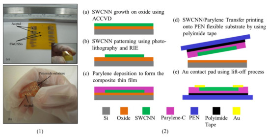
Figure 15.
(1) Flexible strain-sensing devices fabricated on (a) a PEN and (b) PI substrate through transfer printing, with the (2) fabricating process of the single-walled carbon nanonet specimens. Reproduced with permission from [122]; Copyright 2011, IOP Publishing Ltd.
With the use of an adhesive rubber stamp, the ultrathin piezoelectric strain sensor mounted onto an elastomeric substrate could measure the strain based on the voltage output with a resolution close to 10−6 (Figure 16) [118]. The magnetic sensor on the soft membrane can also be fabricated by a single-step direct transfer printing method [121].
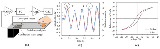
Figure 16.
(a) Schematic illustration of the measurement setup with the fabricated sensor placed next to a commercial strain gauge on the surface of a stainless-steel plate. (b) Comparison of the voltage output from the fabricated sensor with the strain from the commercial strain gauge. (c) Almost identical polarization–voltage hysteresis curves of the piezoelectric strain sensors obtained before and after transfer printing demonstrate the effectiveness and applicability of the technique. Reproduced with permission from [118]; Copyright 2015, the Japan Society of Applied Physics.
3.2. Flexible Transistors
As an indispensable component in active devices, the transistor has been widely used in flexible sensors, displays, medical, and other electronic systems [147]. Transfer printing of single-crystal Si thin film transistors and GaAs microwires onto thin plastic sheets leads to flexible and bendable transistors [52,148] and metal semiconductor field-effect transistors (MESFETs) [147] that are robust to bending deformations. Similarly, transferring high electron mobility transistors to the plastic substrate yields the transistors in a bendable format that is robust to cyclic bending deformations [99]. The initial exploration of the single-crystal Si for stretchable transistors [12,24,149] was started with the creation of wavy Si thin ribbons on elastomeric substrates with the use of the pre-strain strategy. Exploring the technique of water-mediated transfer printing [63,64] also yields a ZnO-based thin film transistor with a high field-effect mobility (Figure 17).
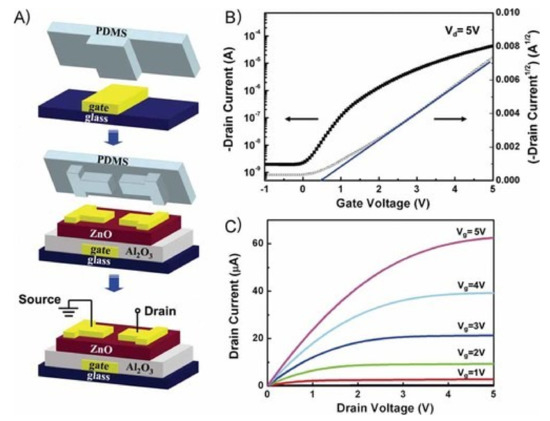
Figure 17.
(a) Schematic illustration of the process of the fabrication of a ZnO-based thin film transistor with the water-mediated transfer printing. Device characterization of the fabricated thin film transistor: (b) Drain current-gate voltage transfer curves and (c) drain current-drain voltage output curves. Reproduced with permission from [64]; Copyright 2009, WILEY-VCH Verlag GmbH & Co., KGaA, Weinheim.
The water-assisted transfer printing method [59] can also be used to transfer the pre-fabricated carbon nanotube (CNT)-based field effect transistors onto the surface of the 3D-printed water-soluble poly(vinyl alcohol) (PVA) substrate (Figure 18) [130]. The almost identical drain current versus gate voltage curves before and after transfer printing demonstrate the high fidelity of the method for fabricating high-performance CNT transistors.
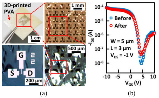
Figure 18.
(a) Optical images of the fabricated carbon nanotube transistors via the water-assisted transfer printing and (b) transfer curves of the drain current versus gate voltage before and after transfer printing. Reproduced with permission from [130]; Copyright 2018, American Chemical Society.
Building on the contact transfer printing [143], the use of an octane and mineral oil mixture serves as a lubricant to help minimize the friction to result in highly ordered and aligned nanowires arrays for diodes and field-effect transistors [150]. Combined with a glass or polyethylene terephthalate (PET) substrate, highly aligned single-walled carbon nanotubes transferred at low temperatures yields a fully transparent thin film transistor [151]. Similarly, transparent field-effect transistors with high optical transmittance can be fabricated by transferring graphene thin films onto elastomeric substrates [152,153].
3.3. Solar Cells
Solar modules consisting of arrays of solar microcells that are fabricated on Si wafers can be integrated into diverse spatial layouts on flexible substrates using transfer printing on a large scale [140]. Comparison of the open-circuit voltages of the devices between those prior and after transfer printing (Figure 19) [154] demonstrates a high degree of power conversion efficiency [6,140].
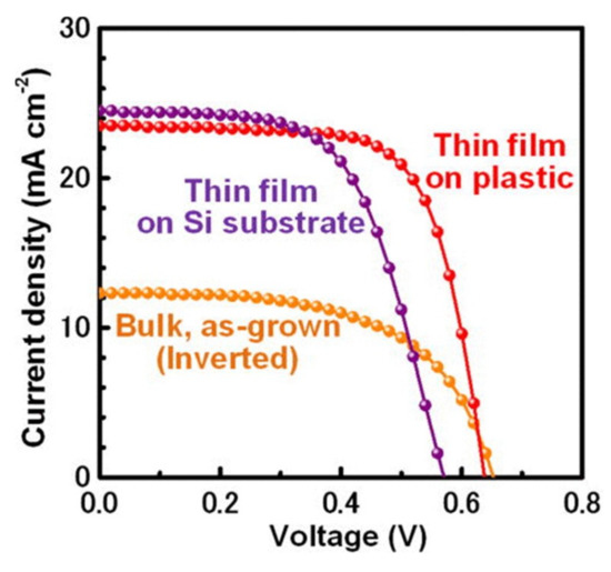
Figure 19.
Current density as a function of the voltage of the highest-efficiency cells for each of the bulk reference cells and the thin-film cells on plastic and Si substrates, respectively. Reproduced with permission from [154]; Copyright 2012, American Institute of Physics.
Building on the WTP method, a peel-and-stick process was developed to build thin-film solar cells (TFSCs) (Figure 20) on a nonconventional substrate, such as the surface of a cell phone, business card, and building window, without compromising its efficiency (Figure 21) [112,155].
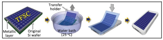
Figure 20.
Schematic illustration of the peel-and-stick process for the fabrication of thin-film solar cells (TFSCs). Reproduced with permission from [112]; Copyright 2012, Macmillan Publishers Limited.
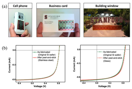
Figure 21.
(a) TFSCs fabricated on a cell phone, business card, and building window, respectively; (b) comparison of the electrical performances of the TFSCs before and after the peel-and-stick process. Reproduced with permission from [112]; Copyright 2012, Macmillan Publishers Limited.
3.4. Flexible Displays
Though the display is a core component of the human-computer interface, the conventional displays remain bulky and rigid. As an emerging technology, flexible displays are light and soft. Currently being explored as one of the key technologies in manufacturing flexible displays, transfer printing enables the transfer of various functional parts, such as the emissive or transport layers, from the growth substrate (donor) onto the device stack [138]. One representative example is the use of transfer printing for the integration of small crystalline-silicon circuits (chiplets) in the active-matrix organic light-emitting-diode (OLED) displays [139,156]. Prepared by the conventional photolithography, hundreds and thousands of chiplets could be transfer printed on the glass substrate via an elastomeric stamp to help build the integrated circuits. The OLED display is then formed over, and connected to, the chiplets. The resulting flexible OLED displays demonstrate an outstanding performance, highlighting the effectiveness of the transfer printing method for the fabrication of flexible displays.
With the help of the intaglio transfer printing method discussed in Section 2.8, wearable red-green-blue and white quantum light-emitting diodes (QLEDs) with a high resolution were demonstrated [89]. The high electroluminescence efficiency in these QLEDs was maintained even after being laminated on crumpled Al foil or on human skin (Figure 22). After multiple printing processes, the red–green–blue diode array was aligned to yield a high-resolution display (ranging from 441 p.p.i. to 2460 p.p.i.). The successful demonstrations clearly confirm the applicability of the intaglio transfer printing method to fabricate ultra-high resolution full-color deformable QLED arrays.
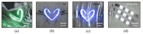
Figure 22.
(a) Optical image of ultra-thin green QLEDs laminated on crumpled Al foil. Photographs of the blue QLEDs laminated on the human skin (b) before and (c) after deformation. (d) Optical image of white QLED arrays laminated on the human skin. Reproduced with permission from [89]; Copyright 2015, Macmillan Publishers Limited.
3.5. Flexible Energy-Harvesting/conversion devices
Because of the intrinsically brittle nature of piezoelectric inorganic materials, piezoelectric energy harvesting and conversion devices fabricated on the conventional substrate are rigid. To exploit the bending property of the thin film device, the highly crystalline piezoelectric ribbons with nanometer scale thicknesses and micrometer-scale widths were transferred from the host substrate onto the pre-strained rubber substrates. Release of the pre-strain yields a stretchable energy harvesting device with a wavy/buckled structure that can be repeatedly stretched and released for multiple cycles without damage (e.g., crack) [103]. Additionally, the piezoelectric ribbons grown on a crystal substrate that were transferred onto the elastomeric substrate over a large area yields energy conversion devices with a high piezoelectric coefficient [104]. The transfer printing method was also explored to manufacture high-performance Pb(Zr,Ti)O3 (PZT) capacitors on plastic substrates for energy storage [109]. After forming the PZT films on the conventional wafer with the sol-gel method, an elastomeric stamp was used to transfer the thin films from the wafer onto the target plastic substrate. The front and backward bending tests (without damage) demonstrated that the flexible PZT thin film capacitor maintained its good electrical properties even under mechanical strain.
3.6. Flexible Electrodes
Using the thermal release transfer printing method, a stretchable neural electrode array with nine channels on a PDMS substrate was fabricated (Figure 23a) [58]. Attaching the device onto the dura mater of a rat in vivo allows the collection of electrocorticography (ECoG) signals (Figure 23b) and the detection of the steady-state visual evoked potentials (SSVEP) response induced by a flash (Figure 23c). Compared to a stainless-steel screw electrode consisting of four channels, the stretchable neural electrode array collected ECoG and SSVEP signals with higher signal-to-noise ratios, because of the conformal contact between the stretchable array and the curvilinear surface of the brain.
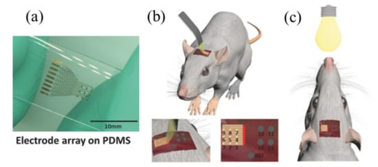
Figure 23.
(a) A stretchable neural electrode array on the PDMS substrate is attached on the curvilinear surface of the brain in the rat to measure the (b) ECoG and (c) SSVEP signal, respectively. Reproduced with permission from [58]; Copyright 2017 by WILEY-VCH Verlag GmbH & Co., KGaA, Weinheim.
3.7. Other Devices
Transfer printing is also explored to fabricate high-performance, stretchable integrated circuits toward personal health monitors and other biomedical devices [125]. Creating a cylindrical nanostructure array on a responsive hydrogel, such as poly(ethylene glycol) dimethacrylate (PEGDMA), provides a new transfer printing strategy [40]. When the hydrogel adhesive film is exposed to water, a significant volume expansion in the PEGDMA structure leads to a large increase in the diameter and height of the hydrogel arrays (Figure 24b). Because of the macroscopic bending in the hydrogel film induced by hydration, the strong surface adhesion strength (≈191 kPa) in the dry state of the hydrogel adhesive sharply decreases (≈0.3 kPa) upon water exposure. Because of the strong adhesion, bringing the hydrogel adhesive into contact with the donor substrate allows the retrieval of the nanomembranes (Figure 24c). After contacting the attached nanomembranes with the receiving substrate, the water dropped on one side penetrates into the space between the hydrogel adhesive and the receiving substrate, which induces the hydrogel to swell (Figure 24d). The swelling-induced bending deformation greatly reduces the adhesion strength at the adhesive/receiver interface, thereby releasing the nanomembranes onto the receiving substrate. The applicability of the smart PEGDMA adhesive for transfer printing was demonstrated by transferring various semiconducting and metallic (e.g., Si, Au, Ag, etc.) micro-/nano-membranes onto different receiving substrates (Figure 25).
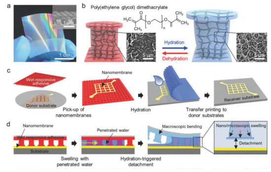
Figure 24.
Schematic illustration of transfer printing with the PEGDMA hydrogel adhesive: (a) Photograph of the fabricated adhesive with a nanostructure array (the inset shows the SEM image); (b) the initial and expanded states of the nanostructures after hydration and dehydration; (c,d) schematic illustration of the transfer printing process using the smart hydrogel adhesive. Reproduced with permission from [40]; Copyright 2018, John Wiley & Sons, Inc.
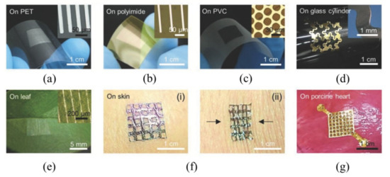
Figure 25.
Different thin film devices transfer printed onto the surfaces of various substrates: (a) Ag nanoribbons, (b) Cu nanoribbons, and (c) Si micro-membranes transfer printed onto the PET, polyimide, and polyvinyl chloride (PVC) films, respectively; (d) the zig-zag shaped Au-polyurethane acrylate (PUA) composite membranes transfer printed onto the curved surface of a glass cylinder; (e) Ag nanoribbons transfer printed onto a plant leaf; (f) Pt-SU-8 composite membranes transfer printed onto human skin and attached firmly under the action of (i) tension and (ii) compression; (g) Au-SU-8 composite membranes transfer printed onto the porcine heart. Reproduced with permission from [40]; Copyright 2018, John Wiley & Sons, Inc.
4. Conclusions and Outlook
Transfer printing technology facilitates the heterogeneous assembly of different materials (e.g., micro/nano-materials) into various functional devices arranged in two-dimensional and three-dimensional layouts. This review describes the recent progress of transfer printing methods involved in the fabrication process of flexible and stretchable electronic devices. Several representative transfer printing methods and their working principles were briefly discussed. With this versatile technology, various materials (e.g., graphene thin films, nano-wires/micro-wires, single-crystal Si ribbons, etc.) and prefabricated device components can be effectively transferred from donor substrates onto receiving substrates with excellent electrical performance. Because each transfer printing method is associated with unique characteristics, careful selection of the transfer printing method for a specific application needs to be conducted, especially in the burgeoning field of flexible and stretchable electronics. Additionally, the optimization of the existing transfer printing methods and development of new methods would motivate continued and expanded efforts in the future.
Among the wide-ranging opportunities for transfer printing technology, one focus may lie in the design and optimization of active, programmable elastomeric stamps for efficient assembly of structures/devices with complicated patterns. Low cost, high speed, high resolution, and reliable transfer printing methods represent other promising areas for future research. The critical geometrical and material parameters that modulate the interfacial adhesion in each method also need to be extensively studied to provide physical insights. The strong interest of small and large companies also requires close examination of the feasibility and applicability of various transfer printing methods in fabricating electronic devices on an industrial scale. A promising route is to explore the roll-to-roll transfer printing process. Major innovations in machine design, process recipes, material handling, and system integration are urgently needed for the achievement of an efficient roll-to-roll transfer printing process. On the other hand, it is highly desirable to explore transfer printing techniques for the integration of functional devices onto curvilinear substrates with various material compositions or even biological materials, which will certainly open up new opportunities in bio-integrated electronics and human-machine interfaces.
Author Contributions
H.Z., W.Q., Q.Y., X.Y., and H.W. wrote the manuscript and assembled the figures. Q.Y. and H.C. led the preparation of the manuscript and contributed to editorial modifications of the overall text.
Funding
The authors would like to acknowledge the financial support from National Natural Science Foundation of China (Grants #: 11872308).
Conflicts of Interest
The authors declare no competing financial interests.
References
- Choi, J.M.; Kim, M.S.; Seol, M.L.; Choi, Y.K. Transfer of functional memory devices to any substrate, physica status solidi (RRL)—Rapid. Res. Lett. 2013, 7, 326–331. [Google Scholar]
- Someya, T.; Kato, Y.; Sekitani, T.; Iba, S.; Noguchi, Y.; Murase, Y.; Kawaguchi, H.; Sakurai, T. Conformable, flexible, large-area networks of pressure and thermal sensors with organic transistor active matrixes. Proc. Natl. Acad. Sci. USA 2005, 102, 12321. [Google Scholar] [CrossRef] [PubMed]
- Crone, B.; Dodabalapur, A.; Lin, Y.Y.; Filas, R.W.; Bao, Z.; Laduca, A.; Sarpeshkar, R.; Katz, H.E.; Li, W. Large-scale complementary integrated circuits based on organic transistors. Nature 2000, 403, 521. [Google Scholar] [CrossRef] [PubMed]
- Forrest, S.R. The path to ubiquitous and low-cost organic electronic appliances on plastic. Nature 2004, 428, 911. [Google Scholar] [CrossRef] [PubMed]
- Navaraj, W.T.; Gupta, S.; Lorenzelli, L.; Dahiya, R. Wafer Scale Transfer of Ultrathin Silicon Chips on Flexible Substrates for High Performance Bendable Systems. Adv. Electron. Mater. 2018, 4, 1700277. [Google Scholar] [CrossRef]
- Caironi, M.; Noh, Y.Y. Large Area and Flexible Electronics; Wiley-VCH Verlag GmbH & Co., KGaA: Hoboken, NJ, USA, 2015. [Google Scholar]
- Liu, X.; Long, Y.-Z.; Liao, L.; Duan, X.; Fan, Z. Large-Scale Integration of Semiconductor Nanowires for High-Performance Flexible Electronics. ACS Nano 2012, 6, 1888–1900. [Google Scholar] [CrossRef]
- Leenen, M.A.M.; Arning, V.; Thiem, H.; Steiger, J.; Anselmann, R. Printable electronics: Flexibility for the future. Phys. Status Solidi A 2009, 206, 588–597. [Google Scholar] [CrossRef]
- Wang, X.; Gu, Y.; Xiong, Z.; Cui, Z.; Zhang, T. Silk-molded flexible, ultrasensitive, and highly stable electronic skin for monitoring human physiological signals. Adv. Mater. 2014, 26, 1336–1342. [Google Scholar] [CrossRef]
- Fan, F.R.; Lin, L.; Zhu, G.; Wu, W.; Zhang, R.; Wang, Z.L. Transparent triboelectric nanogenerators and self-powered pressure sensors based on micropatterned plastic films. Nano Lett. 2012, 12, 3109. [Google Scholar] [CrossRef]
- Pang, C.; Lee, G.Y.; Kim, T.I.; Kim, S.M.; Kim, H.N.; Ahn, S.H.; Suh, K.Y. A flexible and highly sensitive strain-gauge sensor using reversible interlocking of nanofibres. Nat. Mater. 2012, 11, 795–801. [Google Scholar] [CrossRef]
- Khang, D.Y.; Jiang, H.; Huang, Y.; Rogers, J.A. A stretchable form of single-crystal silicon for high-performance electronics on rubber substrates. Science 2006, 311, 208–212. [Google Scholar] [CrossRef] [PubMed]
- Sun, Y.; Kumar, V.; Adesida, I.; Rogers, J.A. Buckled and Wavy Ribbons of GaAs for High-Performance Electronics on Elastomeric Substrates. Adv. Mater. 2006, 18, 2857–2862. [Google Scholar] [CrossRef]
- Sun, Y.; Choi, W.M.; Jiang, H.; Huang, Y.Y.; Rogers, J.A. Controlled buckling of semiconductor nanoribbons for stretchable electronics. Nat. Nanotechnol. 2006, 1, 201. [Google Scholar] [CrossRef] [PubMed]
- Jiang, H.; Khang, D.Y.; Song, J.; Sun, Y.; Huang, Y.; Rogers, J.A. Finite deformation mechanics in buckled thin films on compliant supports. Proc. Natl. Acad. Sci. USA 2007, 104, 15607–15612. [Google Scholar] [CrossRef] [PubMed]
- Jiang, H.; Sun, Y.; Rogers, J.A.; Huang, Y. Mechanics of precisely controlled thin film buckling on elastomeric substrate. Appl. Phys. Lett. 2007, 90, 133119. [Google Scholar] [CrossRef]
- Song, J.; Jiang, H.; Liu, Z.J.; Khang, D.Y.; Huang, Y.; Rogers, J.A.; Lu, C.; Koh, C.G. Buckling of a stiff thin film on a compliant substrate in large deformation. Int. J. Solids Struct. 2008, 45, 3107–3121. [Google Scholar] [CrossRef]
- Chen, C.; Tao, W.; Liu, Z.J.; Zhang, Y.W.; Song, J. Controlled buckling of thin film on elastomeric substrate in large deformation. Theor. Appl. Mech. Lett. 2011, 1, 021001. [Google Scholar] [CrossRef]
- Zaumseil, J.; Meitl, M.A.; Hsu, J.W.P.; Acharya, B.R.; Baldwin, K.W.; Loo, Y.-L.; Rogers, J.A. Three-Dimensional and Multilayer Nanostructures Formed by Nanotransfer Printing. Nano Lett. 2003, 3, 1223–1227. [Google Scholar] [CrossRef]
- Menard, E.; Bilhaut, L.; Zaumseil, J.; Rogers, J.A. Improved Surface Chemistries, Thin Film Deposition Techniques, and Stamp Designs for Nanotransfer Printing. Langmuir 2004, 20, 6871–6878. [Google Scholar] [CrossRef]
- Sun, Y.; Rogers, J.A. Fabricating Semiconductor Nano/Microwires and Transfer Printing Ordered Arrays of Them onto Plastic Substrates. Nano Lett. 2004, 4, 1953–1959. [Google Scholar] [CrossRef]
- Meitl, M.A.; Zhou, Y.; Gaur, A.; Jeon, S.; Usrey, M.L.; Strano, M.S.; Rogers, J.A. Solution Casting and Transfer Printing Single-Walled Carbon Nanotube Films. Nano Lett. 2004, 4, 1643–1647. [Google Scholar] [CrossRef]
- Hur, S.-H.; Park, O.O.; Rogers, J.A. Extreme bendability of single-walled carbon nanotube networks transferred from high-temperature growth substrates to plastic and their use in thin-film transistors. Appl. Phys. Lett. 2005, 86, 243502. [Google Scholar] [CrossRef]
- Meitl, M.A.; Zhu, Z.T.; Kumar, V.; Lee, K.J.; Feng, X.; Huang, Y.Y.; Adesida, I.; Nuzzo, R.G.; Rogers, J.A. Transfer printing by kinetic control of adhesion to an elastomeric stamp. Nat. Mater. 2006, 5, 33–38. [Google Scholar] [CrossRef]
- Feng, X.; Meitl, M.A.; Bowen, A.M.; Huang, Y.; Nuzzo, R.G.; Rogers, J.A. Competing Fracture in Kinetically Controlled Transfer Printing. Langmuir 2007, 23, 12555–12560. [Google Scholar] [CrossRef]
- Yu, J.; Bulović, V. Micropatterning metal electrode of organic light emitting devices using rapid polydimethylsiloxane lift-off. Appl. Phys. Lett. 2007, 91, 043102. [Google Scholar] [CrossRef]
- Park, S.I.; Xiong, Y.; Kim, R.H.; Elvikis, P.; Meitl, M.; Kim, D.H.; Wu, J.; Yoon, J.; Yu, C.J.; Liu, Z. Printed Assemblies of Inorganic Light-Emitting Diodes for Deformable and Semitransparent Displays. Science 2009, 325, 977–981. [Google Scholar] [CrossRef] [PubMed]
- Schmid, H.; Wolf, H.; Allenspach, R.; Riel, H.; Karg, S.; Michel, B.; Delamarche, E. Preparation of Metallic Films on Elastomeric Stamps and Their Application for Contact Processing and Contact Printing. Adv. Funct. Mater. 2003, 13, 145–153. [Google Scholar]
- Bai, W.; Yang, H.; Ma, Y.; Chen, H.; Shin, J.; Liu, Y.; Yang, Q.; Kandela, I.; Liu, Z.; Kang, S.-K. Flexible Transient Optical Waveguides and Surface-Wave Biosensors Constructed from Monocrystalline Silicon. Adv. Mater. 2018, 30, 1801584. [Google Scholar] [CrossRef]
- Andrew, C.; Bowen, A.M.; Huang, Y.; Nuzzo, R.G.; Rogers, J.A. Transfer Printing Techniques for Materials Assembly and Micro/Nanodevice Fabrication. Adv. Mater. 2012, 24, 5284–5318. [Google Scholar]
- Huang, Y.; Li, H.; Chen, Y.; Cai, S.; Zhang, Y.; Lu, B.; Feng, X. Stretchable and flexible photonics/electronics devices and transfer printing. Sci. Sin. Phys. Mech. Astron. 2016, 46, 044607. [Google Scholar] [CrossRef]
- Andrew, C.; Wang, S.; Paulius, E.; Ferreira, P.M.; Huang, Y.; Rogers, J.A. Active, Programmable Elastomeric Surfaces with Tunable Adhesion for Deterministic Assembly by Transfer Printing. Adv. Funct. Mater. 2012, 22, 4476–4484. [Google Scholar]
- Li, R.; Li, Y.; Lü, C.; Song, J.; Saeidpouraza, R.; Fang, B.; Zhong, Y.; Ferreira, P.M.; Rogers, J.A.; Huang, Y. Thermo-mechanical modeling of laser-driven non-contact transfer printing: Two-dimensional analysis. Soft Matter 2012, 8, 7122–7127. [Google Scholar] [CrossRef]
- Zhou, Y.; Hu, L.; Grüner, G. A method of printing carbon nanotube thin films. Appl. Phys. Lett. 2006, 88, 123109. [Google Scholar] [CrossRef]
- Ahn, J.H.; Kim, H.S.; Lee, K.J.; Jeon, S.; Kang, S.J.; Sun, Y.; Nuzzo, R.G.; Rogers, J.A. Heterogeneous Three-Dimensional Electronics by Use of Printed Semiconductor Nanomaterials. Science 2006, 314, 1754–1757. [Google Scholar] [CrossRef] [PubMed]
- Zhu, J.; Xue, M.; Zhao, D.; Zhang, M.; Duan, L.; Qiu, Y.; Cao, T. Facile Fabrication of Metallic Nanostructures by Tunable Cracking and Transfer Printing. Angew. Chem. Int. Ed. 2011, 50, 12478–12482. [Google Scholar] [CrossRef] [PubMed]
- Thanh, Q.N.; Jeong, H.; Kim, J.; Kevek, J.W.; Ahn, Y.H.; Lee, S.; Minot, E.D.; Park, J.-Y. Transfer-Printing of As-Fabricated Carbon Nanotube Devices onto Various Substrates. Adv. Mater. 2012, 24, 4499–4504. [Google Scholar] [CrossRef] [PubMed]
- Winters, S.; Hallam, T.; Nolan, H.; Duesberg, G.S. Production of 3D-shaped graphene via transfer printing. Phys. Status Solidi B 2012, 249, 2515–2518. [Google Scholar] [CrossRef]
- Hohyun, K.; Andrew, C.; Hailong, N.; Agustin, M.; Jeffrey, D.E.; Paul, V.B. Silicon micro-masonry using elastomeric stamps for three-dimensional microfabrication. J. Micromech. Microeng. 2012, 22, 055018. [Google Scholar]
- Yi, H.; Seong, M.; Sun, K.; Hwang, I.; Lee, K.; Cha, C.; Kim, T.-i.; Jeong, H.E. Wet-Responsive, Reconfigurable, and Biocompatible Hydrogel Adhesive Films for Transfer Printing of Nanomembranes. Adv. Funct. Mater. 2018, 28, 1706498. [Google Scholar] [CrossRef]
- Tong, S.; Sun, J.; Yang, J. Printed Thin-Film Transistors: Research from China. ACS Appl. Mater. Interfaces 2018, 10, 25902–25924. [Google Scholar] [CrossRef]
- Feng, X.; Lu, B.; Wu, J.; Lin, Y.; Song, J.; Song, G.; Huang, Y. Review on stretchable and flexible inorganic electronics. Acta Physica Sin. 2014, 63, 1–18. [Google Scholar]
- Kim, T.-H.; Carlson, A.; Ahn, J.-H.; Won, S.M.; Wang, S.; Huang, Y.; Rogers, J.A. Kinetically controlled, adhesiveless transfer printing using microstructured stamps. Appl. Phys. Lett. 2009, 94, 113502. [Google Scholar] [CrossRef]
- Feng, X.; Cheng, H.; Bowen, A.M.; Carlson, A.W.; Nuzzo, R.G.; Rogers, J.A. A Finite-Deformation Mechanics Theory for Kinetically Controlled Transfer Printing. J. Appl. Mech. 2013, 80, 061023. [Google Scholar] [CrossRef]
- Kim, N.; Kang, H.; Lee, J.-H.; Kee, S.; Lee, S.H.; Lee, K. Highly Conductive All-Plastic Electrodes Fabricated Using a Novel Chemically Controlled Transfer-Printing Method. Adv. Mater. 2015, 27, 2317–2323. [Google Scholar]
- Sim, K.; Chen, S.; Li, Y.; Kammoun, M.; Peng, Y.; Xu, M.; Gao, Y.; Song, J.; Zhang, Y.; Ardebili, H.; et al. High Fidelity Tape Transfer Printing Based On Chemically Induced Adhesive Strength Modulation. Sci. Rep. 2015, 5, 16133. [Google Scholar] [CrossRef] [PubMed]
- Jeong, J.W.; Yang, S.R.; Hur, Y.H.; Kim, S.W.; Baek, K.M.; Yim, S.; Jang, H.-I.; Park, J.H.; Lee, S.Y.; Park, C.-O.; et al. High-resolution nanotransfer printing applicable to diverse surfaces via interface-targeted adhesion switching. Nat. Commun. 2014, 5, 5387. [Google Scholar] [CrossRef]
- Song, L.; Ci, L.; Gao, W.; Ajayan, P.M. Transfer Printing of Graphene Using Gold Film. ACS Nano 2009, 3, 1353–1356. [Google Scholar] [CrossRef] [PubMed]
- Reuss, R.H.; Chalamala, B.R.; Moussessian, A.; Kane, M.G.; Kumar, A.; Zhang, D.C.; Rogers, J.A.; Hatalis, M.; Temple, D.; Moddel, G.; et al. Macroelectronics: Perspectives on Technology and Applications. Proc. IEEE 2005, 93, 1239–1256. [Google Scholar] [CrossRef]
- Blanchet, G.B.; Loo, Y.-L.; Rogers, J.A.; Gao, F.; Fincher, C.R. Large area, high resolution, dry printing of conducting polymers for organic electronics. Appl. Phys. Lett. 2003, 82, 463–465. [Google Scholar] [CrossRef]
- Briseno, A.L.; Roberts, M.; Ling, M.-M.; Moon, H.; Nemanick, E.J.; Bao, Z. Patterning organic semiconductors using “dry” poly(dimethylsiloxane) elastomeric stamps for thin film transistors. J. Am. Chem. Soc. 2006, 128, 3880–3881. [Google Scholar] [CrossRef]
- Menard, E.; Nuzzo, R.G.; Rogers, J.A. Bendable single crystal silicon thin film transistors formed by printing on plastic substrates. Appl. Phys. Lett. 2005, 86, 093507. [Google Scholar] [CrossRef]
- Yeom, J.; Shannon, M.A. Detachment Lithography of Photosensitive Polymers: A Route to Fabricating Three-Dimensional Structures. Adv. Funct. Mater. 2010, 20, 289–295. [Google Scholar] [CrossRef]
- Ravikumar, V.; Yi, N.; Vepachedu, V.; Cheng, H. Transfer Printing for Cyber-Manufacturing Systems, in Industrial Internet of Things: Cybermanufacturing Systems; Jeschke, S., Brecher, C., Song, H., Rawat, D.B., Eds.; Springer International Publishing: Cham, Switzerland, 2017; pp. 671–690. [Google Scholar]
- Gao, Y.; Cheng, H. Assembly of Heterogeneous Materials for Biology and Electronics: From Bio-Inspiration to Bio-Integration. J. Electron. Packag. 2017, 139, 020801. [Google Scholar] [CrossRef]
- Linghu, C.; Zhang, S.; Wang, C.; Song, J. Transfer printing techniques for flexible and stretchable inorganic electronics. NPJ Flex. Electron. 2018, 2, 26. [Google Scholar] [CrossRef]
- Cheng, H.; Li, M.; Wu, J.; Carlson, A.; Kim, S.; Huang, Y.; Kang, Z.; Hwang, K.C.; Rogers, J.A. A Viscoelastic Model for the Rate Effect in Transfer Printing. J. Appl. Mech. 2013, 80, 041019. [Google Scholar] [CrossRef]
- Yan, Z.; Pan, T.; Xue, M.; Chen, C.; Cui, Y.; Yao, G.; Huang, L.; Liao, F.; Jing, W.; Zhang, H.; et al. Thermal Release Transfer Printing for Stretchable Conformal Bioelectronics. Adv. Sci. 2017, 4, 1700251. [Google Scholar] [CrossRef]
- Lee, C.H.; Kim, D.R.; Zheng, X. Fabrication of Nanowire Electronics on Nonconventional Substrates by Water-Assisted Transfer Printing Method. Nano Lett. 2011, 11, 3435–3439. [Google Scholar] [CrossRef]
- Lee, C.H.; Kim, D.R.; Zheng, X. Transfer Printing Methods for Flexible Thin Film Solar Cells: Basic Concepts and Working Principles. ACS Nano 2014, 8, 8746–8756. [Google Scholar] [CrossRef]
- Zhao, J.; Guo, Y.; Cai, L.; Li, H.; Wang, K.X.; Cho, I.S.; Lee, C.H.; Fan, S.; Zheng, X. High-Performance Ultrathin BiVO4 Photoanode on Textured Polydimethylsiloxane Substrates for Solar Water Splitting. ACS Energy Lett. 2016, 1, 68–75. [Google Scholar] [CrossRef]
- Wie, D.S.; Zhang, Y.; Kim, M.K.; Kim, B.; Park, S.; Kim, Y.-J.; Irazoqui, P.P.; Zheng, X.; Xu, B.; Lee, C.H. Wafer-recyclable, environment-friendly transfer printing for large-scale thin-film nanoelectronics. Proc. Natl. Acad. Sci. USA 2018, 115, E7236–E7244. [Google Scholar] [CrossRef]
- Lee, B.H.; Cho, Y.H.; Lee, H.; Lee, K.-D.; Kim, S.H.; Sung, M.M. High-Resolution Patterning of Aluminum Thin Films with a Water-Mediated Transfer Process. Adv. Mater. 2007, 19, 1714–1718. [Google Scholar] [CrossRef]
- Oh, K.; Lee, B.H.; Hwang, J.K.; Lee, H.; Im, S.; Sung, M.M. Water-Mediated Al Metal Transfer Printing with Contact Inking for Fabrication of Thin-Film Transistors. Small 2009, 5, 558–561. [Google Scholar] [CrossRef] [PubMed]
- Huang, Y.Y.; Zhou, W.; Hsia, K.J.; Menard, E.; Park, J.-U.; Rogers, J.A.; Alleyne, A.G. Stamp Collapse in Soft Lithography. Langmuir 2005, 21, 8058–8068. [Google Scholar] [CrossRef] [PubMed]
- Hsia, K.J.; Huang, Y.; Menard, E.; Park, J.-U.; Zhou, W.; Rogers, J.; Fulton, J.M. Collapse of stamps for soft lithography due to interfacial adhesion. Appl. Phys. Lett. 2005, 86, 154106. [Google Scholar] [CrossRef]
- Kim, S.; Wu, J.; Carlson, A.; Jin, S.H.; Kovalsky, A.; Glass, P.; Liu, Z.; Ahmed, N.; Elgan, S.L.; Chen, W.; et al. Microstructured elastomeric surfaces with reversible adhesion and examples of their use in deterministic assembly by transfer printing. Proc. Natl. Acad. Sci. USA 2010, 107, 17095–17100. [Google Scholar] [CrossRef] [PubMed]
- Wu, J.; Kim, S.; Chen, W.; Carlson, A.; Hwang, K.-C.; Huang, Y.; Rogers, J.A. Mechanics of reversible adhesion. Soft Matter 2011, 7, 8657–8662. [Google Scholar] [CrossRef]
- Chen, H.; Feng, X.; Huang, Y.; Huang, Y.; Rogers, J.A. Experiments and viscoelastic analysis of peel test with patterned strips for applications to transfer printing. J. Mech. Phys. Solids 2013, 61, 1737–1752. [Google Scholar] [CrossRef]
- Chen, H.; Feng, X.; Chen, Y. Directionally controlled transfer printing using micropatterned stamps. Appl. Phys. Lett. 2013, 103, 151607. [Google Scholar] [CrossRef]
- Jeong, J.; Kim, J.; Song, K.; Autumn, K.; Lee, J. Geckoprinting: Assembly of microelectronic devices on unconventional surfaces by transfer printing with isolated gecko setal arrays. J. R. Soc. Interface 2014, 11, 20140627. [Google Scholar] [CrossRef]
- Yoo, B.; Cho, S.; Seo, S.; Lee, J. Elastomeric Angled Microflaps with Reversible Adhesion for Transfer-Printing Semiconductor Membranes onto Dry Surfaces. ACS Appl. Mater. Interfaces 2014, 6, 19247–19253. [Google Scholar] [CrossRef]
- Carlson, A.; Kim-Lee, H.-J.; Wu, J.; Elvikis, P.; Cheng, H.; Kovalsky, A.; Elgan, S.; Yu, Q.; Ferreira, P.M.; Huang, Y.; et al. Shear-enhanced adhesiveless transfer printing for use in deterministic materials assembly. Appl. Phys. Lett. 2011, 98, 264104. [Google Scholar] [CrossRef]
- Yang, Y.S.; Andrew, C.; Huanyu, C.; Qingmin, Y.; Numair, A.; Jian, W.; Seok, K.; Metin, S.; Ferreira, P.M.; Yonggang, H.; et al. Elastomer Surfaces with Directionally Dependent Adhesion Strength and Their Use in Transfer Printing with Continuous Roll-to-Roll Applications. Adv. Mater. 2012, 24, 2117–2122. [Google Scholar]
- Cheng, H.; Wu, J.; Yu, Q.; Kim-Lee, H.-J.; Carlson, A.; Turner, K.T.; Hwang, K.-C.; Huang, Y.; Rogers, J.A. An analytical model for shear-enhanced adhesiveless transfer printing. Mech. Res. Commun. 2012, 43, 46–49. [Google Scholar] [CrossRef]
- Liu, C.; Qin, H.; Mather, P.T. Review of progress in shape-memory polymers. J. Mater. Chem. 2007, 17, 1543–1558. [Google Scholar] [CrossRef]
- Koerner, H.; Price, G.; Pearce, N.A.; Alexander, M.; Vaia, R.A. Remotely actuated polymer nanocomposites—Stress-recovery of carbon-nanotube-filled thermoplastic elastomers. Nat. Mater. 2004, 3, 115–120. [Google Scholar] [CrossRef]
- Yu, K.; Ge, Q.; Qi, H.J. Reduced time as a unified parameter determining fixity and free recovery of shape memory polymers. Nat. Commun. 2014, 5, 3066. [Google Scholar] [CrossRef]
- Huang, W.M.; Yang, B.; An, L.; Li, C.; Chan, Y.S. Water-driven programmable polyurethane shape memory polymer: Demonstration and mechanism. Appl. Phys. Lett. 2005, 86, 114105. [Google Scholar] [CrossRef]
- Eisenhaure, J.D.; Rhee, S.I.; Al-Okaily, A.M.; Carlson, A.; Ferreira, P.M.; Kim, S. The Use of Shape Memory Polymers for Microassembly by Transfer Printing. J. Microelectromech. Syst. 2014, 23, 1012–1014. [Google Scholar] [CrossRef]
- Eisenhaure, J.D.; Xie, T.; Varghese, S.; Kim, S. Microstructured Shape Memory Polymer Surfaces with Reversible Dry Adhesion. ACS Appl. Mater. Interfaces 2013, 5, 7714–7717. [Google Scholar] [CrossRef]
- Xue, Y.; Zhang, Y.; Feng, X.; Kim, S.; Rogers, J.A.; Huang, Y. A theoretical model of reversible adhesion in shape memory surface relief structures and its application in transfer printing. J. Mech. Phys. Solids 2015, 77, 27–42. [Google Scholar] [CrossRef]
- Saeidpourazar, R.; Li, R.; Li, Y.; Sangid, M.D.; Lu, C.; Huang, Y.; Rogers, J.A.; Ferreira, P.M. Laser-Driven Micro Transfer Placement of Prefabricated Microstructures. J. Microelectromech. Syst. 2012, 21, 1049–1058. [Google Scholar] [CrossRef]
- Saeidpourazar, R.; Sangid, M.D.; Rogers, J.A.; Ferreira, P.M. A prototype printer for laser driven micro-transfer printing. J. Manuf. Process. 2012, 14, 416–424. [Google Scholar] [CrossRef]
- Li, R.; Li, Y.; Lü, C.; Song, J.; Saeidpourazar, R.; Fang, B.; Zhong, Y.; Ferreira, P.M.; Rogers, J.A.; Huang, Y. Axisymmetric thermo-mechanical analysis of laser-driven non-contact transfer printing. Int. J. Fract. 2012, 176, 189–194. [Google Scholar] [CrossRef]
- Ala’a, M.; Rogers, J.A.; Ferreira, P.M. Characterization of Delamination in Laser Micro Transfer Printing. J. Micro Nano-Manuf. 2013, 2, 011002. [Google Scholar]
- Ala’a, M.; Ferreira, P.M. Multi-physics modeling for laser micro-transfer printing delamination. J. Manuf. Process. 2015, 20, 414–424. [Google Scholar]
- Gao, Y.; Li, Y.; Li, R.; Song, J. An Accurate Thermomechanical Model for Laser-Driven Microtransfer Printing. J. Appl. Mech. 2017, 84, 064501. [Google Scholar] [CrossRef]
- Choi, M.K.; Yang, J.; Kang, K.; Kim, D.C.; Choi, C.; Park, C.; Kim, S.J.; Chae, S.I.; Kim, T.-H.; Kim, J.H.; et al. Wearable red-green-blue quantum dot light-emitting diode array using high-resolution intaglio transfer printing. Nat. Commun. 2015, 6, 7149. [Google Scholar] [CrossRef] [PubMed]
- Yu, Q.; chen, F.; Zhou, H.; Yu, X. Mechanical model of electromagnetic-assisted transfer printing stamp containinga four prism cavity. Sci. Sin. Inf. 2018, 48, 713–723. (In Chinese) [Google Scholar] [CrossRef]
- Yu, Q.; Chen, F.; Zhou, H.; Yu, X.; Cheng, H.; Wu, H. Design and Analysis of Magnetic-Assisted Transfer Printing. J. Appl. Mech. 2018, 85, 101009. [Google Scholar] [CrossRef]
- Linghu, C.; Wang, C.; Cen, N.; Wu, J.; Lai, Z.; Song, J. Rapidly tunable and highly reversible bio-inspired dry adhesion for transfer printing in air and a vacuum. Soft Matter 2019, 15, 30–37. [Google Scholar] [CrossRef]
- Hines, D.R.; Mezhenny, S.; Breban, M.; Williams, E.D.; Ballarotto, V.W.; Esen, G.; Southard, A.; Fuhrer, M.S. Nanotransfer printing of organic and carbon nanotube thin-film transistors on plastic substrates. Appl. Phys. Lett. 2005, 86, 163101. [Google Scholar] [CrossRef]
- Sun, Y.; Menard, E.; Rogers, J.A.; Kim, H.-S.; Kim, S.; Chen, G.; Adesida, I.; Dettmer, R.; Cortez, R.; Tewksbury, A. Gigahertz operation in flexible transistors on plastic substrates. Appl. Phys. Lett. 2006, 88, 183509. [Google Scholar] [CrossRef]
- Ko, H.C.; Baca, A.J.; Rogers, J.A. Bulk Quantities of Single-Crystal Silicon Micro-/Nanoribbons Generated from Bulk Wafers. Nano Lett. 2006, 6, 2318–2324. [Google Scholar] [CrossRef] [PubMed]
- Sharma, B.K.; Bongkyun, J.; Eun, L.J.; Sang-Hoon, B.; Woong, K.T.; Hak-Joo, L.; Jae-Hyun, K.; Jong-Hyun, A. Load-Controlled Roll Transfer of Oxide Transistors for Stretchable Electronics. Adv. Funct. Mater. 2013, 23, 2024–2032. [Google Scholar]
- Yu, X.; Yu, S.; Wang, Z.; Ma, D.; Han, Y. Metal printing with modified polymer bonding lithography. Appl. Phys. Lett. 2006, 88, 263517. [Google Scholar] [CrossRef]
- Lee., K.; Motala, M.J.; Meitl, M.A.; Childs, W.R.; Menard, E.; Shim, A.K.; Rogers, J.A.; Nuzzo, R.G. Large-Area, Selective Transfer of Microstructured Silicon: A Printing—Based Approach to High-Performance Thin-Film Transistors Supported on Flexible Substrates. Adv. Mater. 2005, 17, 2332–2336. [Google Scholar]
- Lee, K.J.; Meitl, M.A.; Ahn, J.H.; Rogers, J.A.; Nuzzo, R.G.; Kumar, V.; Adesida, I. Bendable GaN high electron mobility transistors on plastic substrates. J. Appl. Phys. 2006, 100, 1239–1268. [Google Scholar] [CrossRef]
- Mack, S.; Meitl, M.A.; Baca, A.J.; Zhu, Z.-T.; Rogers, J.A. Mechanically flexible thin-film transistors that use ultrathin ribbons of silicon derived from bulk wafers. Appl. Phys. Lett. 2006, 88, 213101. [Google Scholar] [CrossRef]
- Liang, X.; Fu, Z.; Chou, S.Y. Graphene Transistors Fabricated via Transfer-Printing In Device Active-Areas on Large Wafer. Nano Lett. 2007, 7, 3840–3844. [Google Scholar] [CrossRef]
- Kim, H.-S.; Won, S.M.; Ha, Y.-G.; Ahn, J.-H.; Facchetti, A.; Marks, T.J.; Rogers, J.A. Self-assembled nanodielectrics and silicon nanomembranes for low voltage, flexible transistors, and logic gates on plastic substrates. Appl. Phys. Lett. 2009, 95, 183504. [Google Scholar] [CrossRef]
- Qi, Y.; Jafferis, N.T.; Lyons, K.; Lee, C.M.; Ahmad, H.; McAlpine, M.C. Piezoelectric Ribbons Printed onto Rubber for Flexible Energy Conversion. Nano Lett. 2010, 10, 524–528. [Google Scholar] [CrossRef] [PubMed]
- Qi, Y.; Kim, J.; Nguyen, T.D.; Lisko, B.; Purohit, P.K.; McAlpine, M.C. Enhanced Piezoelectricity and Stretchability in Energy Harvesting Devices Fabricated from Buckled PZT Ribbons. Nano Lett. 2011, 11, 1331–1336. [Google Scholar] [CrossRef] [PubMed]
- Kim, R.-H.; Bae, M.-H.; Kim, D.G.; Cheng, H.; Kim, B.H.; Kim, D.-H.; Li, M.; Wu, J.; Du, F.; Kim, H.-S.; et al. Stretchable, Transparent Graphene Interconnects for Arrays of Microscale Inorganic Light Emitting Diodes on Rubber Substrates. Nano Lett. 2011, 11, 3881–3886. [Google Scholar] [CrossRef] [PubMed]
- McAlpine, M.C.; Friedman, R.S.; Lieber, C.M. High-Performance Nanowire Electronics and Photonics and Nanoscale Patterning on Flexible Plastic Substrates. Proc. IEEE 2005, 93, 1357–1363. [Google Scholar] [CrossRef]
- Kim, T.-I.; Jung, Y.H.; Song, J.; Kim, D.; Li, Y.; Kim, H.-s.; Song, I.-S.; Wierer, J.J.; Pao, H.A.; Huang, Y.; et al. High-Efficiency, Microscale GaN Light-Emitting Diodes and Their Thermal Properties on Unusual Substrates. Small 2012, 8, 1643–1649. [Google Scholar] [CrossRef] [PubMed]
- Kim, T.-I.; Lee, S.H.; Li, Y.; Shi, Y.; Shin, G.; Lee, S.D.; Huang, Y.; Rogers, J.A.; Yu, J.S. Temperature- and size-dependent characteristics in ultrathin inorganic light-emitting diodes assembled by transfer printing. Appl. Phys. Lett. 2014, 104, 051901. [Google Scholar] [CrossRef]
- Rho, J.; Kim, S.J.; Heo, W.; Lee, N.E.; Lee, H.S.; Ahn, J.H. PbZrxTi1−xO3 Ferroelectric Thin-Film Capacitors for Flexible Nonvolatile Memory Applications. IEEE Electron. Device Lett. 2010, 31, 1017–1019. [Google Scholar] [CrossRef]
- Koo, M.; Park, K.-I.; Lee, S.H.; Suh, M.; Jeon, D.Y.; Choi, J.W.; Kang, K.; Lee, K.J. Bendable Inorganic Thin-Film Battery for Fully Flexible Electronic Systems. Nano Lett. 2012, 12, 4810–4816. [Google Scholar] [CrossRef]
- Kang, M.-G.; Park, H.J.; Ahn, S.H.; Guo, L.J. Transparent Cu nanowire mesh electrode on flexible substrates fabricated by transfer printing and its application in organic solar cells. Sol. Energy Mater. Sol. Cells 2010, 94, 1179–1184. [Google Scholar] [CrossRef]
- Lee, C.H.; Kim, D.R.; Cho, I.S.; William, N.; Wang, Q.; Zheng, X. Peel-and-Stick: Fabricating Thin Film Solar Cell on Universal Substrates. Sci. Rep. 2012, 2, 1000. [Google Scholar] [CrossRef]
- Lin, Y.; Xu, H.Y.; Wang, Z.Q.; Cong, T.; Liu, W.Z.; Ma, H.L.; Liu, Y.C. Transferable and flexible resistive switching memory devices based on PMMA films with embedded Fe3O4 nanoparticles. Appl. Phys. Lett. 2017, 110, 193503. [Google Scholar] [CrossRef]
- Son, D.; Lee, J.; Qiao, S.; Ghaffari, R.; Kim, J.; Lee, J.E.; Song, C.; Kim, S.J.; Lee, D.J.; Jun, S.W.; et al. Multifunctional wearable devices for diagnosis and therapy of movement disorders. Nat. Nanotechnol. 2014, 9, 397. [Google Scholar] [CrossRef] [PubMed]
- McAlpine, M.C.; Ahmad, H.; Wang, D.; Heath, J.R. Highly ordered nanowire arrays on plastic substrates for ultrasensitive flexible chemical sensors. Nat. Mater. 2007, 6, 379–384. [Google Scholar] [CrossRef] [PubMed]
- Webb, R.C.; Bonifas, A.P.; Behnaz, A.; Zhang, Y.; Yu, K.J.; Cheng, H.; Shi, M.; Bian, Z.; Liu, Z.; Kim, Y.-S.; et al. Ultrathin conformal devices for precise and continuous thermal characterization of human skin. Nat. Mater. 2013, 12, 938. [Google Scholar] [CrossRef] [PubMed]
- Huang, X.; Cheng, H.; Chen, K.; Zhang, Y.; Zhang, Y.; Liu, Y.; Zhu, C.; Ouyang, S.c.; Kong, G.W.; Yu, C.; et al. Epidermal Impedance Sensing Sheets for Precision Hydration Assessment and Spatial Mapping. IEEE Trans. Biomed. Eng. 2013, 60, 2848–2857. [Google Scholar] [CrossRef]
- Takahiro, Y.; Hironao, O.; Toshihiro, I.; Takeshi, K. Manufacturing process for piezoelectric strain sensor sheet involving transfer printing methods. Jpn. J. Appl. Phys. 2015, 54, 10ND08. [Google Scholar]
- Jidong, S.; Xinming, L.; Huanyu, C.; Zhuangjian, L.; Lingyu, Z.; Tingting, Y.; Zhaohe, D.; Zengguang, C.; Enzheng, S.; Long, Y.; et al. Graphene Reinforced Carbon Nanotube Networks for Wearable Strain Sensors. Adv. Funct. Mater. 2016, 26, 2078–2084. [Google Scholar]
- O’Neill, J.; Lu, J.; Dockter, R.; Kowalewski, T. Stretchable, Flexible, Scalable Smart Skin Sensors for Robotic Position and Force Estimation. Sensors 2018, 18, 953. [Google Scholar] [CrossRef]
- Melzer, M.; Karnaushenko, D.; Lin, G.; Baunack, S.; Makarov, D.; Schmidt, O.G. Direct transfer of magnetic sensor devices to elastomeric supports for stretchable electronics. Adv. Mater. 2015, 27, 1333–1338. [Google Scholar] [CrossRef] [PubMed]
- Hsu, C.C.; Chao, R.M.; Liu, C.W.; Steven, Y.L. Evaluation of the gauge factor for single-walled carbon nanonets on the flexible plastic substrates by nano-transfer-printing. J. Micromech. Microeng. 2011, 21, 075012. [Google Scholar] [CrossRef]
- Lee, W.S.; Choi, J.-h.; Park, I.; Lee, J. Room-Temperature Compressive Transfer Printing of Nanowires for Nanoelectronic Devices. Langmuir 2012, 28, 17851–17858. [Google Scholar] [CrossRef] [PubMed]
- Chen, J.H.; Ishigami, M.; Jang, C.; Hines, D.R.; Fuhrer, M.S.; Williams, E.D. Printed Graphene Circuits. Adv. Mater. 2007, 19, 3623–3627. [Google Scholar] [CrossRef]
- Kim, D.H.; Ahn, J.H.; Choi, W.M.; Kim, H.S.; Kim, T.H.; Song, J.; Huang, Y.Y.; Liu, Z.; Lu, C.; Rogers, J.A. Strechable and foldable silicon integrated circuits. Science 2008, 320, 507–511. [Google Scholar] [CrossRef] [PubMed]
- Cho, K.H.; Gunchul, S.; Shuodao, W.; Stoykovich, M.P.; Won, L.J.; Dong-Hun, K.; Sook, H.J.; Yonggang, H.; Keh-Chih, H.; Rogers, J.A. Curvilinear Electronics Formed Using Silicon Membrane Circuits and Elastomeric Transfer Elements. Small 2009, 5, 2703–2709. [Google Scholar]
- Dae-Hyeong, K.; Yun-Soung, K.; Jian, W.; Zhuangjian, L.; Jizhou, S.; Hoon-Sik, K.; Huang, Y.Y.; Keh-Chih, H.; Rogers, J.A. Ultrathin Silicon Circuits With Strain-Isolation Layers and Mesh Layouts for High-Performance Electronics on Fabric, Vinyl, Leather, and Paper. Adv. Mater. 2009, 21, 3703–3707. [Google Scholar]
- Dae-Hyeong, K.; Zhuangjian, L.; Yun-Soung, K.; Jian, W.; Jizhou, S.; Hoon-Sik, K.; Yonggang, H.; Keh-chih, H.; Yongwei, Z.; Rogers, J.A. Optimized Structural Designs for Stretchable Silicon Integrated Circuits. Small 2009, 5, 2841–2847. [Google Scholar]
- Kim, D.-H.; Song, J.; Choi, W.M.; Kim, H.-S.; Kim, R.-H.; Liu, Z.; Huang, Y.Y.; Hwang, K.-C.; Zhang, Y.-W.; Rogers, J.A. Materials and noncoplanar mesh designs for integrated circuits with linear elastic responses to extreme mechanical deformations. Proc. Natl. Acad. Sci. USA 2008. [Google Scholar] [CrossRef]
- Yoon, J.; Han, J.; Choi, B.; Lee, Y.; Kim, Y.; Park, J.; Lim, M.; Kang, M.-H.; Kim, D.H.; Kim, D.M.; et al. Three-Dimensional Printed Poly(vinyl alcohol) Substrate with Controlled On-Demand Degradation for Transient Electronics. ACS Nano 2018, 12, 6006–6012. [Google Scholar] [CrossRef]
- Chang, J.-K.; Chang, H.-P.; Guo, Q.; Koo, J.; Wu, C.-I.; Rogers, J.A. Biodegradable Electronic Systems in 3D, Heterogeneously Integrated Formats. Adv. Mater. 2018, 30, 1704955. [Google Scholar] [CrossRef]
- Chang, J.-K.; Fang, H.; Bower, C.A.; Song, E.; Yu, X.; Rogers, J.A. Materials and processing approaches for foundry-compatible transient electronics. Proc. Natl. Acad. Sci. USA 2017, 114, E5522–E5529. [Google Scholar] [CrossRef]
- Yu, K.J.; Kuzum, D.; Hwang, S.-W.; Kim, B.H.; Juul, H.; Kim, N.H.; Won, S.M.; Chiang, K.; Trumpis, M.; Richardson, A.G.; et al. Bioresorbable silicon electronics for transient spatiotemporal mapping of electrical activity from the cerebral cortex. Nat. Mater. 2016, 15, 782. [Google Scholar] [CrossRef]
- Kim, D.-H.; Viventi, J.; Amsden, J.J.; Xiao, J.; Vigeland, L.; Kim, Y.-S.; Blanco, J.A.; Panilaitis, B.; Frechette, E.S.; Contreras, D.; et al. Dissolvable films of silk fibroin for ultrathin conformal bio-integrated electronics. Nat. Mater. 2010, 9, 511. [Google Scholar] [CrossRef] [PubMed]
- Hwang, S.-W.; Tao, H.; Kim, D.-H.; Cheng, H.; Song, J.-K.; Rill, E.; Brenckle, M.A.; Panilaitis, B.; Won, S.M.; Kim, Y.-S.; et al. A physically transient form of silicon electronics. Science 2012, 337, 1640–1644. [Google Scholar] [CrossRef] [PubMed]
- Hwang, S.-W.; Kim, D.-H.; Tao, H.; Kim, T.-i.; Kim, S.; Yu, K.J.; Panilaitis, B.; Jeong, J.-W.; Song, J.-K.; Omenetto, F.G.; et al. Materials and Fabrication Processes for Transient and Bioresorbable High-Performance Electronics. Adv. Funct. Mater. 2013, 23, 4087–4093. [Google Scholar] [CrossRef]
- Hwang, S.-W.; Song, J.-K.; Huang, X.; Cheng, H.; Kang, S.-K.; Kim, B.H.; Kim, J.-H.; Yu, S.; Huang, Y.; Rogers, J.A. High-Performance Biodegradable/Transient Electronics on Biodegradable Polymers. Adv. Mater. 2014, 26, 3905–3911. [Google Scholar] [CrossRef] [PubMed]
- Koo, J.H.; Kim, D.C.; Shim, H.J.; Kim, T.-H.; Kim, D.-H. Flexible and Stretchable Smart Display: Materials, Fabrication, Device Design, and System Integration. Adv. Funct. Mater. 2018, 28, 1801834. [Google Scholar] [CrossRef]
- Cok, R.S.; Hamer, J.W.; Bower, C.A.; Menard, E.; Bonafede, S. AMOLED displays with transfer-printed integrated circuits. J. Soc. Inf. Disp. 2011, 19, 335–341. [Google Scholar] [CrossRef]
- Yoon, J.; Baca, A.J.; Park, S.-I.; Elvikis, P.; Geddes Iii, J.B.; Li, L.; Kim, R.H.; Xiao, J.; Wang, S.; Kim, T.-H.; et al. Ultrathin silicon solar microcells for semitransparent, mechanically flexible and microconcentrator module designs. Nat. Mater. 2008, 7, 907. [Google Scholar] [CrossRef]
- Lin, Q.; Huang, H.; Jing, Y.; Fu, H.; Chang, P.; Li, D.; Yao, Y.; Fan, Z. Flexible photovoltaic technologies. J. Mater. Chem. C 2014, 2, 1233–1247. [Google Scholar] [CrossRef]
- Yu, C.; Wang, Z.; Yu, H.; Jiang, H. A stretchable temperature sensor based on elastically buckled thin film devices on elastomeric substrates. Appl. Phys. Lett. 2009, 95, 141912. [Google Scholar] [CrossRef]
- Javey, A.; Nam; Friedman, R.S.; Yan, H.; Lieber, C.M. Layer-by-Layer Assembly of Nanowires for Three-Dimensional, Multifunctional Electronics. Nano Lett. 2007, 7, 773–777. [Google Scholar] [CrossRef] [PubMed]
- Loo, Y.-L.; Willett, R.L.; Baldwin, K.W.; Rogers, J.A. Additive, nanoscale patterning of metal films with a stamp and a surface chemistry mediated transfer process: Applications in plastic electronics. Appl. Phys. Lett. 2002, 81, 562–564. [Google Scholar] [CrossRef]
- Loo, Y.-L.; Willett, R.L.; Baldwin, K.W.; Rogers, J.A. Interfacial Chemistries for Nanoscale Transfer Printing. J. Am. Chem. Soc. 2002, 124, 7654–7655. [Google Scholar] [CrossRef] [PubMed]
- Loo, Y.-L.; Lang, D.V.; Rogers, J.A.; Hsu, J.W.P. Electrical Contacts to Molecular Layers by Nanotransfer Printing. Nano Lett. 2003, 3, 913–917. [Google Scholar] [CrossRef]
- Sun, Y.; Kim, S.; Adesida, I.; Rogers, J.A. Bendable GaAs metal-semiconductor field-effect transistors formed with printed GaAs wire arrays on plastic substrates. Appl. Phys. Lett. 2005, 87, 083501. [Google Scholar] [CrossRef]
- Menard, E.; Lee, K.J.; Khang, D.-Y.; Nuzzo, R.G.; Rogers, J.A. A printable form of silicon for high performance thin film transistors on plastic substrates. Appl. Phys. Lett. 2004, 84, 5398–5400. [Google Scholar] [CrossRef]
- Baca, A.J.; Meitl, M.A.; Ko, H.C.; Mack, S.; Kim, H.S.; Dong, J.; Ferreira, P.M.; Rogers, J.A. Printable Single-Crystal Silicon Micro/Nanoscale Ribbons, Platelets and Bars Generated from Bulk Wafers. Adv. Funct. Mater. 2007, 17, 3051–3062. [Google Scholar] [CrossRef]
- Fan, Z.; Ho, J.C.; Jacobson, Z.A.; Yerushalmi, R.; Alley, R.L.; Razavi, H.; Javey, A. Wafer-Scale Assembly of Highly Ordered Semiconductor Nanowire Arrays by Contact Printing. Nano Lett. 2008, 8, 20–25. [Google Scholar] [CrossRef]
- Ishikawa, F.N.; Chang, H.-k.; Ryu, K.; Chen, P.-c.; Badmaev, A.; Gomez De Arco, L.; Shen, G.; Zhou, C. Transparent Electronics Based on Transfer Printed Aligned Carbon Nanotubes on Rigid and Flexible Substrates. ACS Nano 2009, 3, 73–79. [Google Scholar] [CrossRef]
- Lee, S.-K.; Kim, B.J.; Jang, H.; Yoon, S.C.; Lee, C.; Hong, B.H.; Rogers, J.A.; Cho, J.H.; Ahn, J.-H. Stretchable Graphene Transistors with Printed Dielectrics and Gate Electrodes. Nano Lett. 2011, 11, 4642–4646. [Google Scholar] [CrossRef]
- Li, X.; Cai, W.; An, J.; Kim, S.; Nah, J.; Yang, D.; Piner, R.; Velamakanni, A.; Jung, I.; Tutuc, E.; et al. Large-area synthesis of high-quality and uniform graphene films on copper foils. Science 2009, 324, 1312–1314. [Google Scholar] [CrossRef] [PubMed]
- Tanabe, K.; Watanabe, K.; Arakawa, Y. Flexible thin-film InAs/GaAs quantum dot solar cells. Appl. Phys. Lett. 2012, 100, 192102. [Google Scholar] [CrossRef]
- Lee, C.H.; Kim, J.-H.; Zou, C.; Cho, I.S.; Weisse, J.M.; Nemeth, W.; Wang, Q.; van Duin, A.C.T.; Kim, T.-S.; Zheng, X. Peel-and-Stick: Mechanism Study for Efficient Fabrication of Flexible/Transparent Thin-film Electronics. Sci. Rep. 2013, 3, 2917. [Google Scholar] [CrossRef] [PubMed]
- Bower, C.A.; Menard, E.; Bonafede, S.; Hamer, J.W.; Cok, R.S. Transfer-Printed Microscale Integrated Circuits for High Performance Display Backplanes. IEEE Trans. Compon. Packag. Manuf. Technol. 2011, 1, 1916–1922. [Google Scholar] [CrossRef]


© 2019 by the authors. Licensee MDPI, Basel, Switzerland. This article is an open access article distributed under the terms and conditions of the Creative Commons Attribution (CC BY) license (http://creativecommons.org/licenses/by/4.0/).