Article

Ferroelectric Diode Effect with Temperature Stability of Double Perovskite Bi2NiMnO6 Thin Films

School of Physics Optoelectric Engineering, Guangdong University of Technology, Guangzhou Higher Education Mega Center, Guangzhou 510006, China
*
Author to whom correspondence should be addressed.
Nanomaterials 2019, 9(12), 1783; https://doi.org/10.3390/nano9121783
Submission received: 20 November 2019 / Revised: 5 December 2019 / Accepted: 10 December 2019 / Published: 15 December 2019

Abstract

:
Double perovskite Bi2NiMnO6 (BNMO) thin films grown on p-Si (100) substrates with LaNiO3 (LNO) buffer layers were fabricated using chemical solution deposition. The crystal structure, surface topography, surface chemical state, ferroelectric, and current-voltage characteristics of BNMO thin films were investigated. The results show that the nanocrystalline BNMO thin films on p-Si substrates without and with LNO buffer layer are monoclinic phase, which have antiferroelectric-like properties. The composition and chemical state of BNMO thin films were characterized by X-ray photoelectron spectroscopy. In the whole electrical property testing process, when the BNMO/p-Si heterojunction changed into a BNMO/LNO/p-Si heterojunction, the diode behavior of a single diode changing into two tail to tail diodes was observed. The conduction mechanism and temperature stability were also discussed.

1. Introduction

In the past few decades, electronic devices prepared using a semiconductor have become an important research project in the field of materials science [1,2,3,4]. These devices have garnered attention for their practical applications, such as magnetoresistance, photodetectors, p-n diodes and thin film transistors [5,6]. Bi2NiMnO6 has been widely studied as a multiferroic material. The ferromagnetic and ferroelectric Bi2NiMnO6 was successfully prepared at 6 GPa as reported by Azuma et al. [7]. Low temperature (about 100 K) ferroelectric properties in pulsed laser-deposition drive Bi2NiMnO6 thin films on (001)-oriented SrTiO3 single crystal substrates were reported by Sakai et al. [8]. The phase transition temperature of epitaxial Bi2NiMnO6 thin films affected by single crystal substrates was studied using Raman spectroscopy [9]. The magnetodielectric effect was obtained in single-phase and epitaxial thin film of multiferroic Bi2NiMnO6, as reported by Padhan et al. and Rathi et al. [10,11,12]. The ferroelectric behavior and magnetic exchange interaction effect of Bi2NiMnO6 with the electric polarization 19.01 μC/cm2 was reported by Zhao et al. [13]. Theoretical and experimental results confirm that Bi2NiMnO6 thin films are multiferroic materials [8,14,15,16,17,18]. The ferroelectric and current leakage characteristics of La-doped Bi2NiMnO6 and Bi2NiMnO6 thin film was reported by Li et al. [19].
However, the ferroelectric diode effect and temperature stability of Bi2NiMnO6 thin film has never been reported. Therefore, in this work, a thin film of Bi2NiMnO6 was growth on p-Si and LaNiO3/p-Si substrates using chemical solution deposition technology, the ferroelectric diode effect and temperature stability of Bi2NiMnO6 thin film was first investigated, as was the conduction mechanism.

2. Materials and Methods

The Bi2NiMnO6 (abbreviated as BNMO) precursor was prepared by dissolving nitrogen salt, bismuth, manganese acetate, and nickel acetate in a ratio of 2.2:1:1 in ethylene glycol solution [16]. The excess of 10% bismuth was to prevent evaporation of the film during the drying and annealing process. Three milliliters of acetic acid was added to the solution to prevent precipitation. The precursor BNMO concentration is 0.2 M. The LaNiO3 (LNO) precursor was prepared by dissolving nickel acetate and lanthanum nitrate in a ratio of 1:1 in ethylene glycol solution and the resulting concentration was 0.3 M. The 5 mL acetone acetate stabilizer was also added to the precursor. The precursors were then aged for 3 days. The wet LNO/p-Si thin film was synthesized by a spin-coating process at a rate of 2500 rpm for 15 s. The LNO/p-Si substrate was made using a drying process at 573 K for 5 min and an annealing process at 973 k for 30 min. The BNMO/p-Si and BNMO/LNO/p-Si heterojunctions are prepared using the spin coating process at 3000 rpm for 15 s, the dry process at 573 K for 5 min and annealing process at 973 K for 10 min by rapid thermal annealing (RTA) in air atmosphere. A gold electrode with a diameter of 0.3 mm was plated on the surface of the film sample by a small high vacuum coater to form a film capacitor structure.
The crystal structure analysis was measured using XRD (Bruker D8 Advance, AXS, Germany) and the chemical states were examined using X-ray photoelectron spectroscopy (XPS, Escalab 250Xi, Sussex, UK). The surface topography and elemental analysis were performed with the field emission scanning electron microscope (FE-SEM, SU8220, Hitachi, Japan). The ferroelectric properties of the BNMO thin films were measured with a ferroelectric test system (Radiant Technologies Precision Workstation, Albuquerque, NM, USA). The current-voltage characteristic was measured with a Keithley 2400 system.

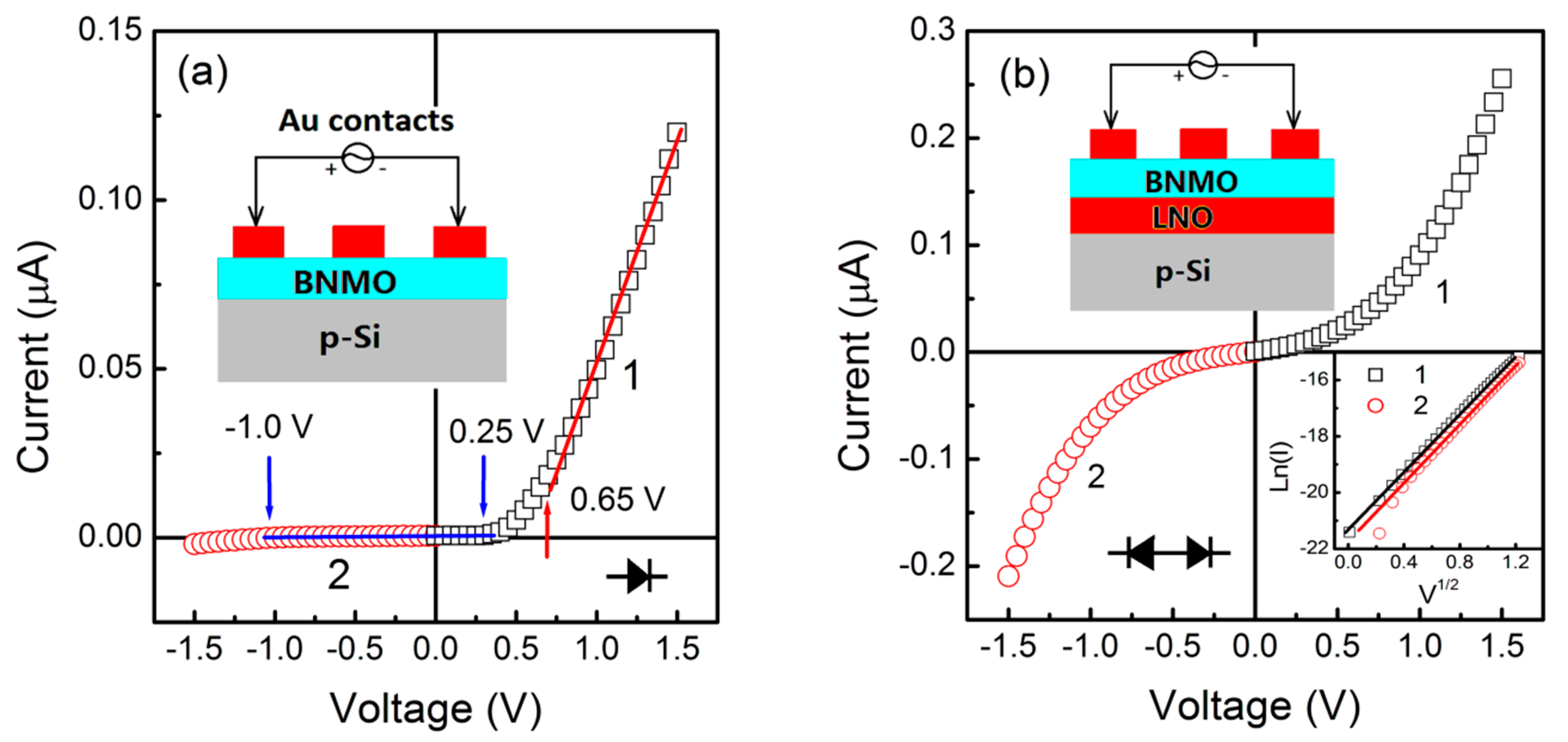
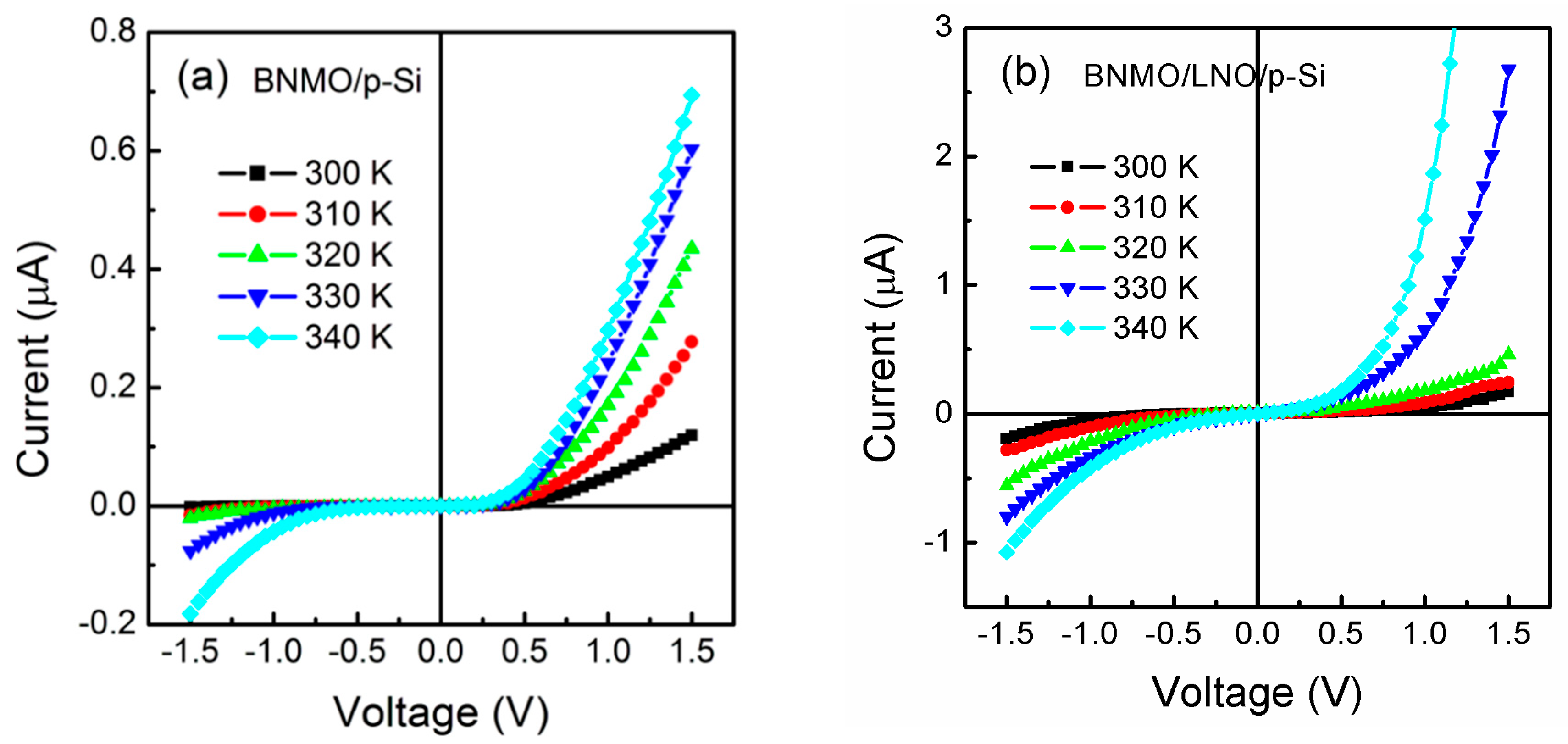
3. Results and Discussion

The XRD patterns are shown in Figure 1. From Figure 1, there are six peaks at (100), (110), (111), (200), (210) and (211), the crystal structure of LNO grown on p-Si can be judged by PDF card of 33-0710 as a cubic phase. The crystal structure of BNMO film grown on p-Si substrate without and with LNO can be determined by diffraction angles of 23.62° and 31.18°. It has the monoclinic structure reported by Azuma et al. [7]. The unit cell of BNMO was considered to be similar to BiMnO3. The three possible transition metal sites of M1, M2, and M3 were filled with Bi3+, Ni2+ and Mn4+ cations and the Mn4+–O2−–Ni2+ chemical links and Bi3+–O2− links were the main chain segment. The diffraction angle of 27.58°and 29.22° matches the results of Li et al. [19], and it is a monoclinic structure with C2 space group [20]. In theory, The NiO6 and MnO6 octahedral of BNMO are isotropic and do not cause distortion.
Figure 2 show the surface and cross-section topographies of BNMO thin film and BNMO/LNO thin film grown p-Si substrates, respectively. From Figure 2a,b it can be clearly observed from the surface topography that the grain size of BNMO/p-Si thin film is nearly 15 nm, but the BNMO/LNO/p-Si thin film is nearly 10 nm. The BNMO thin film was formed by the Mn4+ cations and Ni2+ cations, and the thin films was annealed at air atmosphere for only 10 min. Therefore, the growth of crystal grains is relatively difficult, resulting in a small grain size. Observed from the cross-section images, it can be obtained that the thickness of the BNMO layer growth on the p-Si substrata is nearly 100 nm (see Figure 2c), the BNMO layer on LNO/p-Si substrate is 140 nm (see Figure 2d). The different film thickness of the BNMO layers may be caused by the different adhesion of LNO and Si to the solution and the first layer, respectively.
The XPS spectra of Ni 2p and Mn 2p are shown in Figure 3. The binding energy of Mn 2p3/2 and Mn 2p1/2 of the BNMO/p-Si heterojunctions was 641.35 eV and 653.2 eV [21]. The binding energy of Mn 2p3/2 and Mn 2p1/2 of the BNMO/LNO heterojunction was 641.6 eV and 653.45 eV. The binding energy of Ni 2p3/2 and Ni 2p1/2 of the BNMO/p-Si heterojunction was 872.45 eV and 861.3 eV [22]. The binding energy of Ni 2p3/2 and Ni 2p1/2 of the BNMO/LNO/p-Si heterojunction was 855.1 eV and 872.55 eV.
The XPS spectrum is subject to peak processing. The binding energy of 638.85 eV, 641.65 eV, and 644.25 eV of the BNMO/p-Si heterojunction and 638.25 eV, 641.5 eV, and 643.95 eV of the BNMO/LNO/p-Si heterojunction indicates the Mn2+, Mn4+ and Mn6+ cation. The binding energy of 855 eV and 857.65 eV of the BNMO/p-Si heterojunction and 855 eV and 857.2 eV of the BNMO/LNO/p-Si heterojunction shows the Ni2+ and Ni3+ cation. The ion ratio of Mn2+:Mn4+:Mn6+ on BNMO/p-Si thin film is 0.15:1:0.3 and for BNMO/LNO/p-Si thin film is 0.16:1:0.27. The ratio of Ni2+:Ni3+ on the BNMO/p-Si heterojunction and on the BNMO/LNO heterojunction is 1:0.22 and 1:0.24, respectively. By analyzing the XPS spectrum, a variety of Ni, Mn ions are found in the BNMO heterojunction device. The cubic crystal structure of NiO and BiMnO3 octahedral crystallites interferes with the formation of pure phase monoclinic crystals and causes crystal defects.
The room temperature polarization-electric field (P-E) properties are shown in Figure 4. The results show that the two films have antiferroelectric-like properties. The saturated polarization (2Ps), remnant polarization (2Pr), and coercive field (Ec) of BNMO/LNO/Si thin film were 0.875 µC/cm2, 0.150 µC/cm2, and 40.0 kV/cm, and 1.03 µC/cm2, 0.202 µC/cm2, and 38.4 kV/cm, respectively for BNMO/Si and BNMO/LNO/Si thin films at 500 Hz. The ferroelectric polarization was enhanced by using LNO as a buffer layer. The room temperature ferroelectric polarization phenomenon could be due to the incompletely symmetric monoclinic structure preventing the ferroelectric domain from flipping. It is a pinning effect caused by the interaction of defect dipoles in the BNMO layer. The BNMO growth on the LNO/p-Si substrate is a nanocrystalline state, resulting in more lattice defects, preventing the deformation of the crystal [7].
The current-voltage characteristics of BNMO/Si and BNMO/LNO/Si thin films are shown in Figure 5. From Figure 5a, we know that from 0 to −1.0 V and from 0 to 0.25 V, the current hardly changed with the increase of absolute voltage value, when the voltage increases from −1.0 to −1.5 V, the current increased, and when the voltage increased from 0.65 to 1.5 V, the current increased rapidly. The results show typical diode characteristics.
The BNMO/p-Si heterojunction exhibited rectification effect behavior of p-n junction. It is a forward-conducting heterojunction device with an ON/OFF ratio (R = Ion/Ioff) of 65. The n-type semiconductor properties of BNMO have not been reported. It can be inferred from the results, and the process of converting Mn2+ ions into Mn4+ ions can release electrons.
As the bottom electrodes of the LNO grew on the p-Si substrate, the rectification effect of the forward conduction was forcibly converted into a reverse conduction rectification effect, and the ON/OFF ratio is increased to 1.4. The result shows two tail to tail diodes. The cubic phase of LNO acted as an n-type semiconductor to release electrons, while the nano-crystallinity of the BNMO layer defects acted as a hole-absorbing electron [23,24,25].The Schottky emission mechanism is determined by the linear relationship of Ln(I) versus V1/2 [26,27]. If the relationship is linear, this is due to the thermionic emission by holes, vacancies and defects [28,29,30,31,32], respectively. The restricted behavior of the interface and the hole trapping behavior are considered to be a case of the Schottky emission mechanism, as expected with linear relationship of Ln(I) versus V1/2 for the BNMO/LNO/p-Si heterojunction (see the inset of Figure 5b). Therefore, the large ON/OFF ratio of the BNMO/LNO/p-Si heterojunction is caused by the hole of the BNMO layer being filled.
The voltage-current characteristics measured at different temperatures were shown in Figure 6. The conductivity of the BNMO/p-Si heterojunction and the BNMO/LNO/p-Si heterojunction was increased due to increased test temperature. The ON/OFF ratio of the BNMO/p-Si heterojunction is decreased from 65 to 3.8, and the ON/OFF ratio of the BNMO/LNO/p-Si heterojunction is increased from 1.4 to 13.4. The result can be interpreted with the thermion emission effect of Schottky diodes [33,34,35,36]. The electrons are excited by the lattice defects caused by the heat. Therefore, the conductivity of the film increases. At the same time, the space charge accumulated at the interface of the heterojunction is also subject to thermal radiation. The BNMO/p-Si heterojunction is excited by thermal radiation, causing the electrons of the defect to be excited, forming a space charge region at the interface of the heterojunction, and finally the rectification effect is improved. The BNMO/LNO/p-Si heterojunction is thermally radiated, and the electron trapping ability of the hole is weakened, resulting in the rectification effect being weakened.

4. Conclusions

In conclusion, the BNMO thin films on Si and LNO/Si substrates show a monoclinic phase with C2 space group and the porosity of BNMO thin film with LNO layer is smaller than without, resulting in a larger ferroelectric polarization. The conduction mechanism of the BNMO/Si and BNMO/LNO/Si heterojunctions were dominated by Ohmic conduction and Schottky emission mechanisms, respectively. In the case of temperature rise, the rectification effect of BNMO/Si will decrease due to the energy of the hole trapping electrons being weakened and the rectification effect of the BNMO/LNO/p-Si heterojunction will increase due to the charge accumulation, respectively. XPS testing shows that BNMO synthesized under normal pressure is a material with the coexistence of different valence cations.

Author Contributions

Author X.-G.T. and Q.-X.L., conceptualized the idea. The test was helped by the W.-M.Z., W.-P.L. and T.-D.C. The draft of the manuscript was reviewed and revised by W.-M.Z. and X.-G.T. The work was supported and supervised by Q.-X.L., Y.-P.J. and W.-H.L. All authors read and approved the final manuscript.

Funding

This research was funded by “the National Natural Science Foundation of China (Grant Nos. 11574057 and 51604087)”, “the Guangdong Provincial Natural Science Foundation of China (Grant No. 2016A030313718)”, and “the Science and Technology Program of Guangdong Province of China (Grant Nos. 2016A010104018 and 2017A010104022)”.

Conflicts of Interest

The authors declare no conflict of interest.

References

  1. Park, S.; Lee, B.; Bae, B.; Chai, J.; Lee, S.; Kim, C. Ambipolar thin-film transistors based on organic semiconductor blend. Synth. Met. 2019, 253, 40–47. [Google Scholar] [CrossRef]
  2. Shiryaev, A.O.; Rozanov, K.N.; Vyzulin, S.A.; Kevraletin, A.L.; Syr’ev, N.E.; Vyzulin, E.S.; Lahderanta, E.; Maklakov, S.A.; Granovsky, A.B. Magnetic resonances and microwave permeability in thin Fe films on flexible polymer substrates. J. Magn. Magn. Mater. 2018, 461, 76–81. [Google Scholar] [CrossRef]
  3. Makhlouf, M.M. Preparation and optical characterization of β-MnO2 nano thin films for application in heterojunction photodiodes. Sens. Actuators A Phys. 2018, 279, 145–156. [Google Scholar] [CrossRef]
  4. Munshi, A.H.; Sasidharan, N.; Pinkayan, S.; Barth, K.L.; Sampath, W.S.; Ongsakul, W. Thin-film CdTe photovoltaics—The technology for utility scale sustainable energy generation. Sol. Energy 2018, 173, 511–516. [Google Scholar] [CrossRef]
  5. Yin, L.; Wang, C.; Li, L.; Shen, Q.; Zhang, L. Large room temperature magnetoresistance in La0.9Sr0.1MnO3 thin films. J. Alloys Compd. 2018, 730, 327–332. [Google Scholar] [CrossRef]
  6. Mitta, S.B.; Reddeppa, M.; Vellampatti, S.; Dugasani, S.R.; Yoo, S.; Lee, S.; Kim, M.D.; Park, S.H. Gold nanoparticle-embedded DNA thin films for ultraviolet photodetectors. Sens. Actuators B Chem. 2018, 275, 137–144. [Google Scholar] [CrossRef]
  7. Azuma, M.; Takata, K.; Saito, T.; Ishiwata, S.; Shimakawa, Y.; Takano, M. Designed Ferromagnetic, Ferroelectric Bi2NiMnO6. J. Am. Chem. Soc. 2005, 127, 8889–8892. [Google Scholar] [CrossRef]
  8. Sakai, M.; Masuno, A.; Kan, D.; Hashisaka, M.; Takata, K.; Azuma, M.; Takano, M.; Shimakawa, Y. Multiferroic thin film of Bi2NiMnO6 with ordered double-perovskite structure. Appl. Phys. Lett. 2007, 90, 072903. [Google Scholar] [CrossRef] [Green Version]
  9. Iliev, M.N.; Padhan, P.; Gupta, A. Temperature-dependent Raman study of multiferroic Bi2NiMnO6 thin films. Phys. Rev. B 2008, 77, 172303. [Google Scholar] [CrossRef]
  10. Padhan, P.; LeClair, P.; Gupta, A.; Srinivasan, G. Magnetodielectric response in epitaxial thin films of multiferroic Bi2NiMnO6. J. Phys. Condens. Matter 2008, 20, 355003. [Google Scholar] [CrossRef]
  11. Padhan, P.; LeClair, P.; Gupta, A.; Subramanian, M.A.; Srinivasan, G. Magnetodielectric effect in Bi2NiMnO6-La2NiMnO6 superlattices. J. Phys. Condens. Matter 2009, 21, 306004. [Google Scholar] [CrossRef] [PubMed] [Green Version]
  12. Rathi, A.; Anshul, A.; Gupta, A.; Rout, P.K.; Maurya, K.K.; Kotnala, R.K.; Pant, R.P.; Basheed, G.A. Large low-field magnetodielectric response in multiferroic Bi2NiMnO6 thin film. J. Phys. D Appl. Phys. 2017, 50, 135006. [Google Scholar] [CrossRef]
  13. Zhao, H.J.; Chen, X.M. First-principles study on the differences of possible ferroelectric behavior and magnetic exchange interaction between Bi2NiMnO6 and La2NiMnO6. AIP Adv. 2012, 2, 042143. [Google Scholar] [CrossRef]
  14. Ciucivara, A.; Sahu, B.; Kleinman, L. Density functional study of multiferroic Bi2NiMnO6. Phys. Rev. B 2007, 76, 064412. [Google Scholar] [CrossRef]
  15. Shimakawa, Y.; Kan, D.; Kawai, M.; Sakai, M.; Inoue, S.; Azuma, M.; Kimura, S.; Sakata, O. Direct observation of B-site ordering in multiferroic Bi2NiMnO6 thin film. Jpn. J. Appl. Phys. 2007, 46, L845–L847. [Google Scholar] [CrossRef]
  16. Bahoosh, S.G.; Wesselinowa, J.M.; Trimper, S. The magnetoelectric effect and double-perovskite structure. Phys. Status Solidi B 2012, 249, 1602–1606. [Google Scholar] [CrossRef]
  17. Zhao, H.J.; Liu, X.Q.; Chen, X.M. Density functional investigations on electronic structures, magnetic ordering and ferroelectric phase transition in multiferroic Bi2NiMnO6. AIP Adv. 2012, 2, 022115. [Google Scholar] [CrossRef] [Green Version]
  18. Dieguez, D.; Iniguez, J. Multiferroic Bi2NiMnO6 thin films: A computational prediction. Phys. Rev. B 2017, 95, 085129. [Google Scholar] [CrossRef] [Green Version]
  19. Li, W.P.; Liu, Q.X.; Tang, X.G.; Lai, J.L.; Jiang, Y.P. Low leakage current in (Bi0.95La0.05)2NiMnO6 double-perovskite thin films prepared by chemical solution deposition. Mater Lett. 2014, 120, 23–25. [Google Scholar] [CrossRef]
  20. Harijan, P.K.; Singh, A.; Upadhyay, C.; Pandey, D. Néel transition in the multiferroic BiFeO3-0.25PbTiO3 nanoparticles with anomalous size effect. J. Appl. Phys. 2019, 125, 024102. [Google Scholar] [CrossRef]
  21. Cerrato, J.M.; Hochella, M.F.; Knocke, W.R.; Dietrich, A.M.; Cromer, T.F. Use of XPS to Identify the Oxidation State of Mn in Solid Surfaces of Filtration Media Oxide Samples from Drinking Water Treatment Plants. Environ. Sci. Technol. 2010, 44, 5881–5886. [Google Scholar] [CrossRef] [PubMed]
  22. Amaya, Á.A.; González, C.A.; Niño-Gómez, M.E.; Martínez, O.F. XPS fitting model proposed to the study of Ni and La in deactivated FCC catalysts. J. Electron. Spectrosc. 2019, 233, 5–10. [Google Scholar] [CrossRef]
  23. Afroz, K.; Moniruddin, M.; Bakranov, N.; Kudaibergenov, S.; Nuraje, N.A. Heterojunction strategy to improve the visible light sensitive water splitting performance of photocatalytic materials. J. Mater. Chem. A 2018, 6, 21696–21718. [Google Scholar] [CrossRef]
  24. Chang, C.M.; Hsu, C.H.; Liu, Y.W.; Chien, T.C.; Sung, C.H.; Yeh, P.H. Interface engineering: Broadband light and low temperature gas detection abilities using a nano-heterojunction device. Nanoscale 2015, 7, 20126–20131. [Google Scholar] [CrossRef] [PubMed]
  25. Kumar, S.G.; Rao, K.S.R.K. Physics and chemistry of CdTe/CdS thin film heterojunction photovoltaic devices: Fundamental and critical aspects. Energy Environ. Sci. 2014, 7, 45–102. [Google Scholar] [CrossRef]
  26. Dietz, G.W.; Waser, R. Charge injection in SrTiO3 thin films. Thin Solid Film. 1997, 299, 53–58. [Google Scholar] [CrossRef]
  27. Wang, Y.G.; Tang, X.G.; Liu, Q.X.; Jiang, Y.P.; Jiang, L.L. Room temperature tunable multiferroic properties in sol-gel derived nanocrystalline Sr(Ti1−xFex)O3−δ thin films grown on LaNiO3 buffered silicon substrates. Nanomaterials 2017, 7, 264. [Google Scholar] [CrossRef] [Green Version]
  28. Barnett, C.J.; Mourgelas, V.; McGettrick, J.D.; Maffeis, T.G.G.; Barron, A.R.; Cobley, R.J. The effects of vacuum annealing on the conduction characteristics of ZnO nanorods. Mater. Lett. 2019, 243, 144–147. [Google Scholar] [CrossRef] [Green Version]
  29. Lee, H.S. Electrokinetic analyses in biofilm anodes: Ohmic conduction of extracellular electron transfer. Bioresour. Technol. 2018, 256, 509–514. [Google Scholar] [CrossRef]
  30. Abbaszadeh, D.; Blom, P.W.M. Efficient Blue Polymer Light-Emitting Diodes with Electron-Dominated Transport Due to Trap Dilution. Adv. Electron. Mater. 2016, 2, 1500406. [Google Scholar] [CrossRef]
  31. Rani, V.; Sharma, A.; Kumar, P.; Singh, B.; Ghosh, S. Charge transport mechanism in copper phthalocyanine thin films with and without traps. RSC Adv. 2017, 7, 54911–54919. [Google Scholar] [CrossRef] [Green Version]
  32. Shah, S.S.; Hayat, K.; Ali, S.; Rasool, K.; Iqbal, Y. Conduction mechanisms in lanthanum manganite nanofibers. Mat. Sci. Semicon. Proc. 2019, 90, 65–71. [Google Scholar] [CrossRef]
  33. Perello, D.J.; Lim, S.C.; Chae, S.J.; Lee, I.; Kim, M.J.; Lee, Y.H.; Yun, M. Thermionic Field Emission Transport in Carbon Nanotube Transistors. ACS Nano 2011, 5, 1756–1760. [Google Scholar] [CrossRef] [PubMed]
  34. Rodriguez-Nieva, J.F.; Dresselhaus, M.S.; Levitov, L.S. Thermionic Emission and Negative dI/dV in Photoactive Graphene Heterostructures. Nano Lett. 2015, 15, 1451–1456. [Google Scholar] [CrossRef] [Green Version]
  35. Chen, C.C.; Aykol, M.; Chang, C.C.; Levi, A.F.J.; Cronin, S.B. Graphene-Silicon Schottky Diodes. Nano Lett. 2011, 11, 1863–1867. [Google Scholar] [CrossRef]
  36. Lao, C.S.; Liu, J.; Gao, P.; Zhang, L.; Davidovic, D.; Tummala, R.; Wang, Z.L. ZnO Nanobelt/Nanowire Schottky Diodes Formed by Dielectrophoresis Alignment across Au Electrodes. Nano Lett. 2006, 6, 263–266. [Google Scholar] [CrossRef] [Green Version]
Figure 1. The XRD patterns of LNO, BNMO/LNO and BNMO thin films on p-Si substrates.
Nanomaterials 09 01783 g001
Figure 2. The surface topography and cross-section images: (a,c) for BNMO/p-Si, (b,d) for BNMO/LNO/p-Si.
Nanomaterials 09 01783 g002
Figure 3. The fitted narrow-scan spectra for (a) Mn 2p and (b) Ni 2p.
Nanomaterials 09 01783 g003
Figure 4. The typical hysteresis loops of the BNMO/Si and BNMO/LNO/Si thin films measured at 500 Hz.
Nanomaterials 09 01783 g004
Figure 5. I-V characteristics of BNMO thin films without (a) and with (b) a LNO buffer layer on p-Si substrates. Insets show the schematics of the diode cell used for measurement.
Nanomaterials 09 01783 g005
Figure 6. The I-V characteristics of BNMO thin films (a) without and (b) with a LNO buffer layer on p-Si substrates measured at different temperatures.
Nanomaterials 09 01783 g006

