Facile Synthesis of Methylammonium Lead Iodide Perovskite with Controllable Morphologies with Enhanced Luminescence Performance


Abstract

1. Introduction
2. Materials and Methods
2.1. Materials
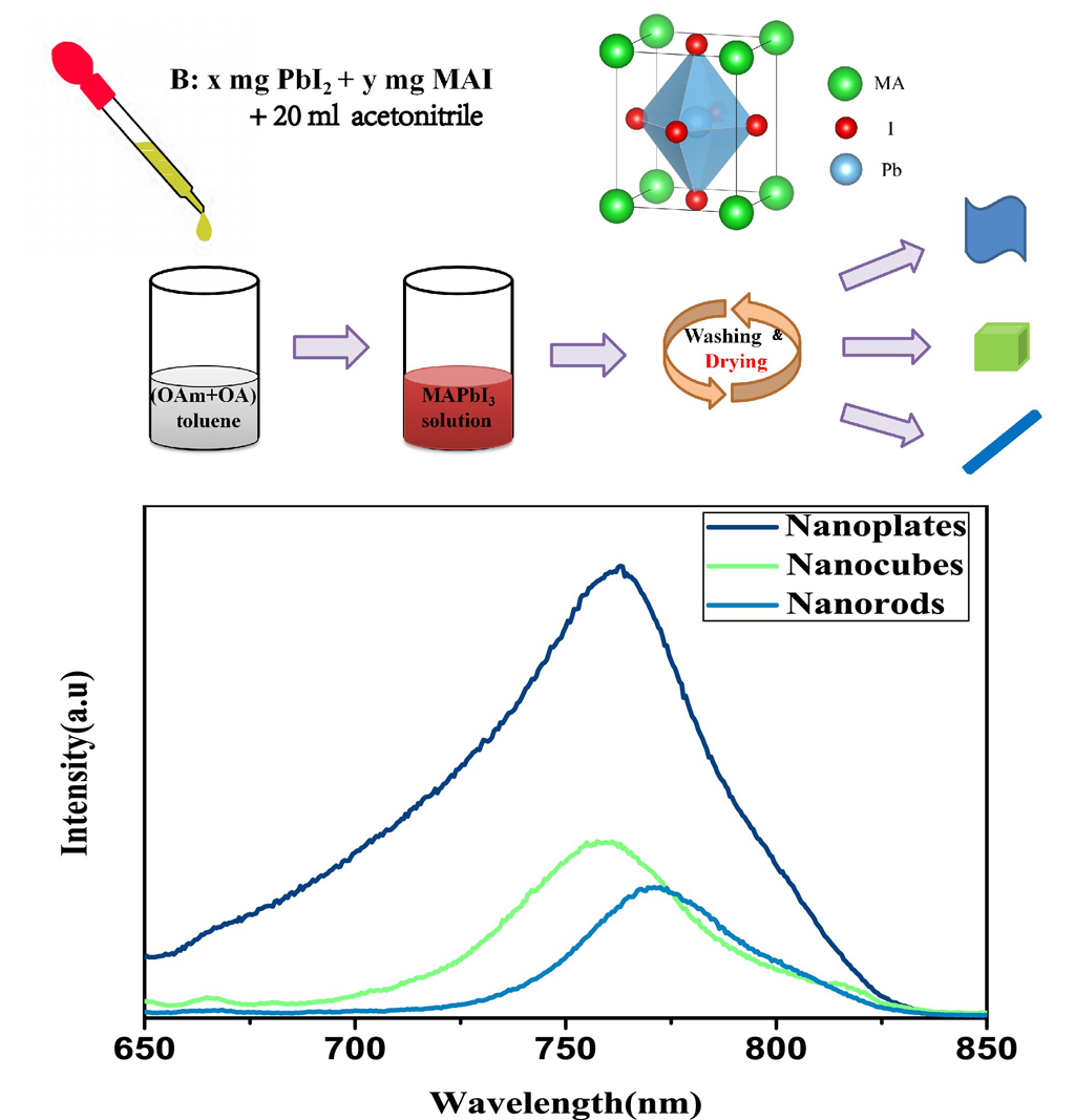
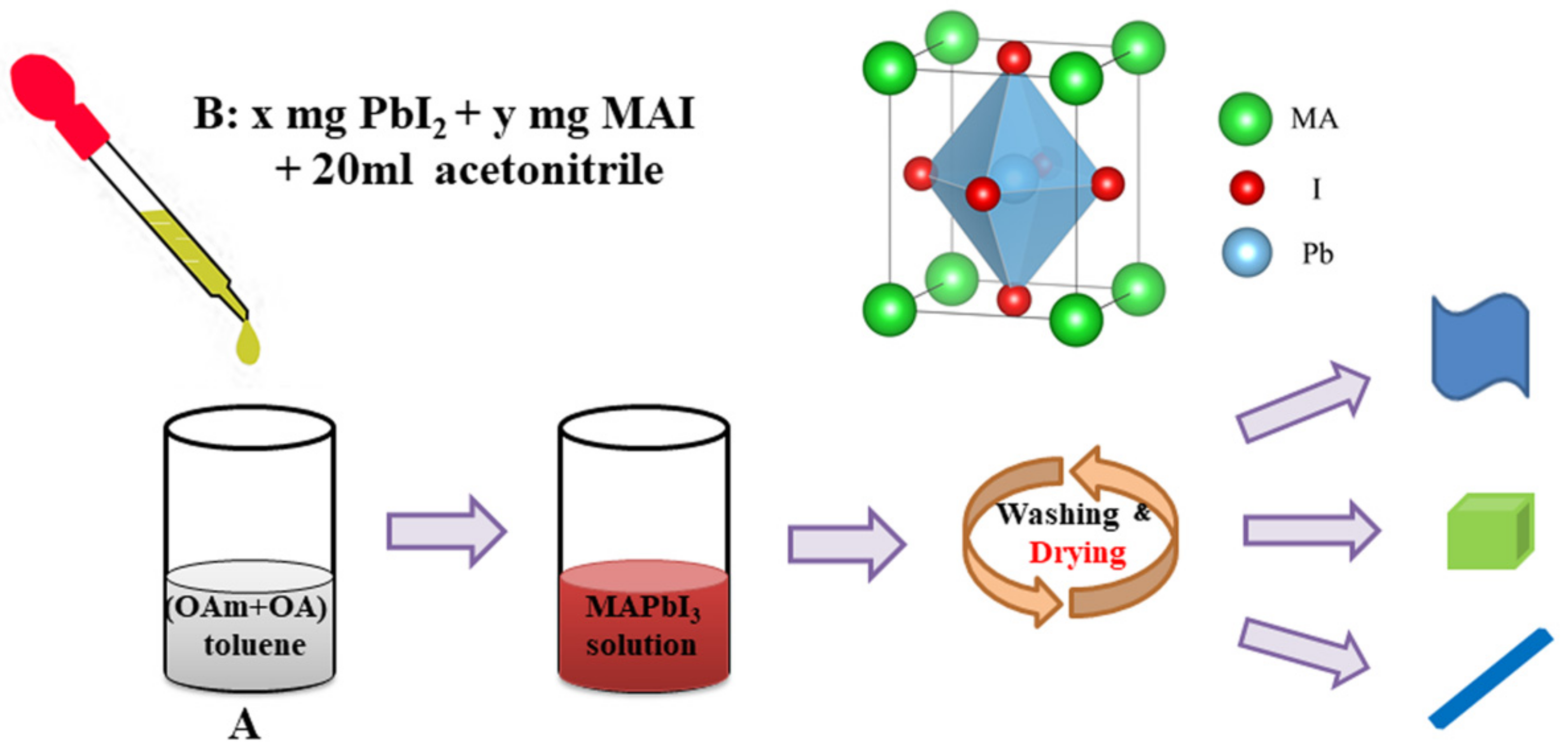
2.2. Synthesis
2.3. Characterization
3. Results
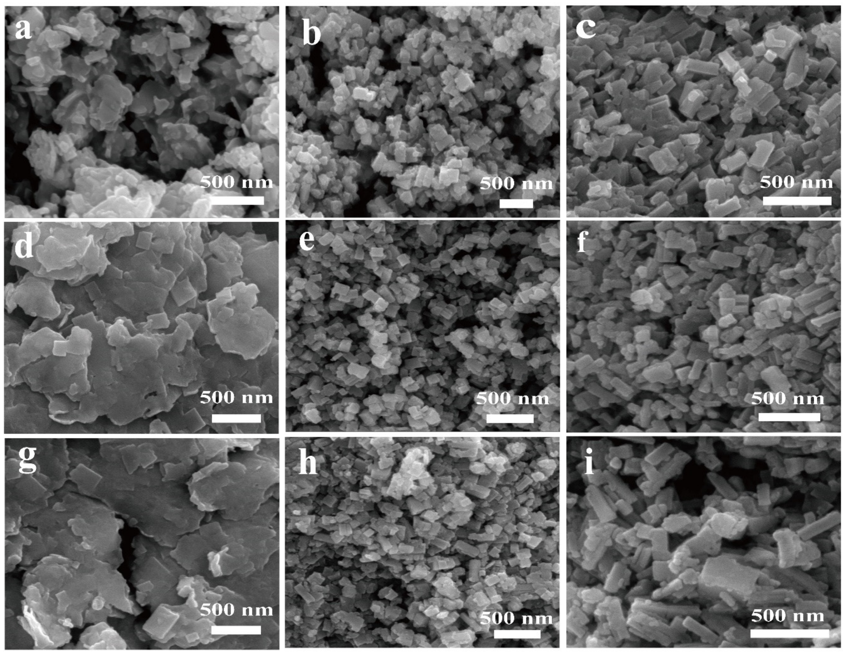
3.1. Influence of Reactant Concentration on Morphology of Resulted Samples
3.2. Influences of the Dropping Rate on the Morphology of MAPbI3 Nanosamples
3.3. Influence of Drying Temperature on the Size of Resulted Samples
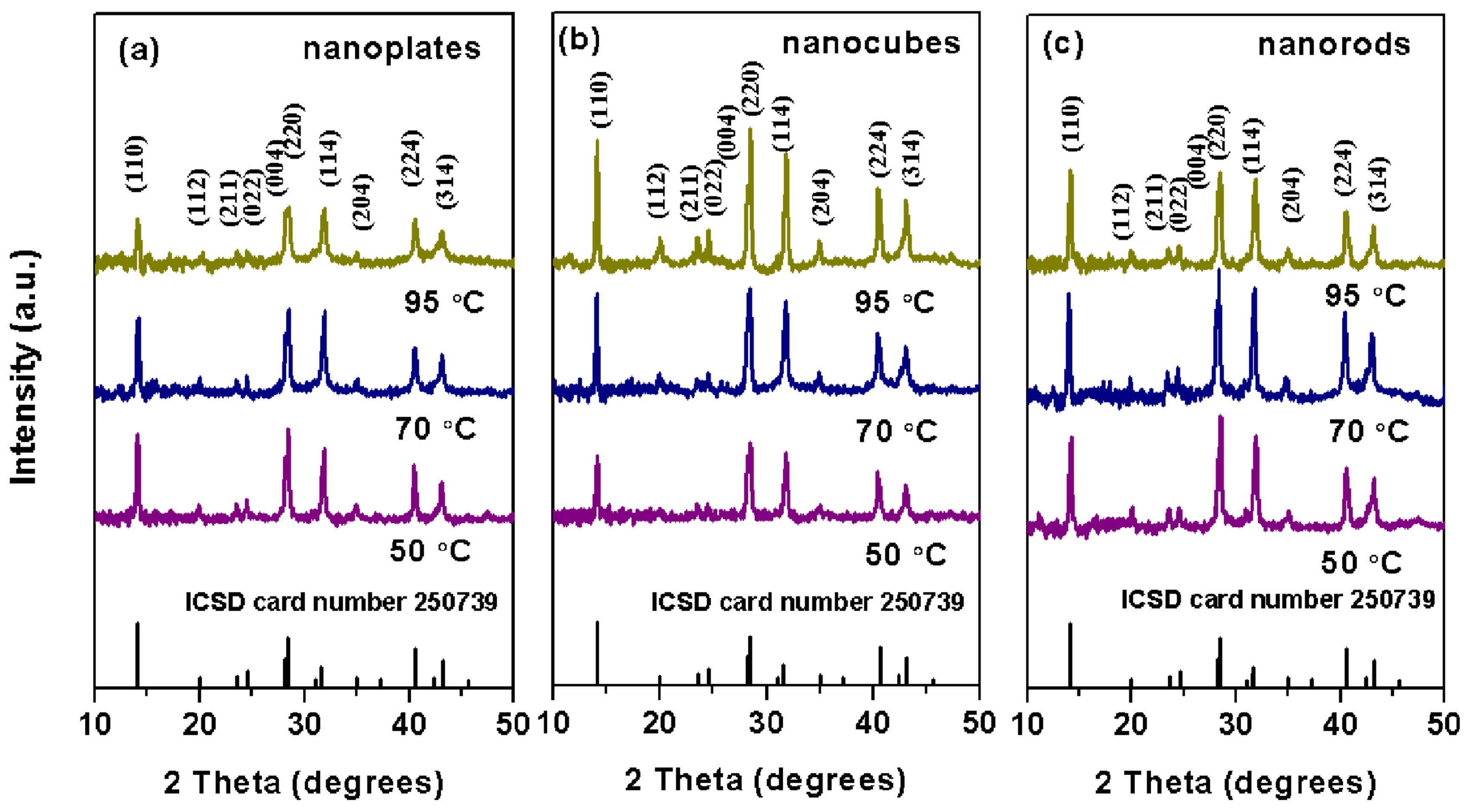
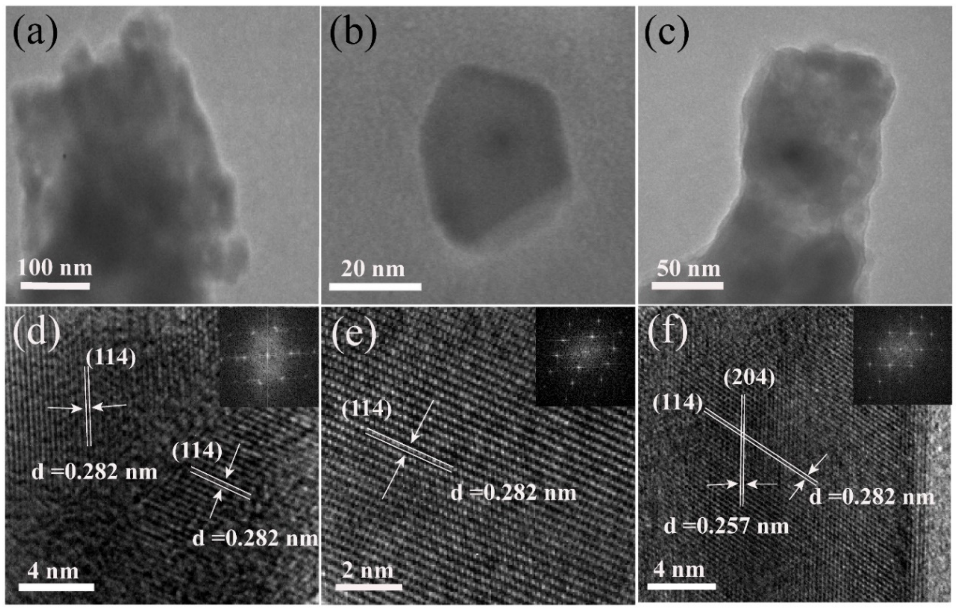
3.4. Analysis of the Crystal Structure
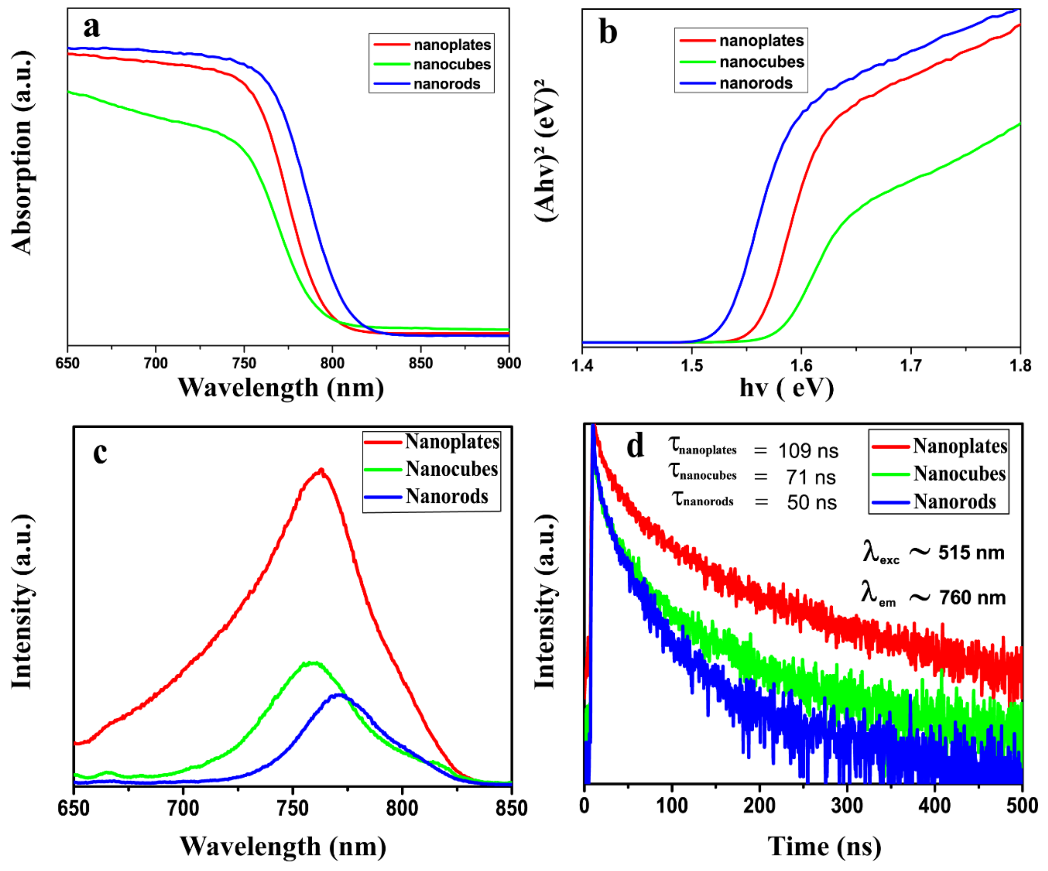
3.5. Influence Morphology on the Optical Properties of MAPbI3 Nanosamples
4. Conclusions
Supplementary Materials
Author Contributions
Funding
Conflicts of Interest
References
- Kojima, A.; Teshima, K.; Shirai, Y.; Miyasaka, T. Organometal Halide Perovskites as Visible-Light Sensitizers for Photovoltaic Cells. J. Am. Chem. Soc. 2009, 131, 6050–6051. [Google Scholar] [CrossRef] [PubMed]
- Lee, M.M.; Teuscher, J.; Miyasaka, T.; Murakami, T.N.; Snaith, H.J. Efficient Hybrid Solar Cells Based on Meso-Superstructured Organometal Halide Perovskites. Science 2012, 338, 643–647. [Google Scholar] [CrossRef] [PubMed]
- Park, N.G. Perovskite solar cells an emerging photovoltaic technology. Mater. Today 2014, 18, 65–72. [Google Scholar] [CrossRef]
- Gao, P.; Grätzel, M.; Nazeeruddin, M.K. Organohalide Lead Perovskites for Photovoltaic Applications. Energy Environ. Sci. 2014, 7, 2448–2463. [Google Scholar] [CrossRef]
- Green, M.A.; Ho-Baillie, A.; Snaith, H.J. The emergence of perovskite solar cells. Nat. Photonics 2014, 8, 506–514. [Google Scholar] [CrossRef]
- Ling, Y.; Yuan, Z.; Tian, Y.; Wang, X.; Wang, J.C.; Xin, Y.; Hanson, K.; Ma, B.; Gao, H. Bright Light-Emitting Diodes Based on Organometal Halide Perovskite Nanoplatelets. Adv. Mater. 2016, 28, 305–311. [Google Scholar] [CrossRef]
- Fu, Y.; Zhu, H.; Schrader, A.W.; Liang, D.; Ding, Q.; Joshi, P.; Hwang, L.; Zhu, X.; Jin, S. Nanowire lasers of formamidinium lead halide perovskites and their stabilized alloys with improved stability. Nano Lett. 2016, 16, 1000–1008. [Google Scholar] [CrossRef]
- Yang, T.; Zheng, Y.; Du, Z.; Liu, W.; Yang, Z.; Gao, F.; Wang, L.; Chou, K.C.; Hou, X.; Yang, W. Superior Photodetectors Based on All-Inorganic Perovskite CsPbI3 Nanorods with Ultrafast Response and High Stability. ACS Nano 2018, 12, 1611–1617. [Google Scholar] [CrossRef]
- Jeon, N.J.; Na, H.; Shin, H.W.; Seok, S.I.; Jung, E.H.; Lee, J.; Yang, T.Y.; Seo, J.; Lee1, Y.G. A fluorene-terminated hole-transpor. Nat. Energy 2018, 3, 682. [Google Scholar] [CrossRef]
- Yoshikawa, K.; Kawasaki, H.; Yoshida, W.; Irie, T.; Konishi, K.; Nakano, K.; Uto, T.; Adachi, D.; Kanematsu, M.; Uzu, H.; et al. Silicon Heterojunction Solar Cell with Interdigitated Back Contacts for a Photoconversion Efficiency over 26%. Nat. Energy 2017, 2, 17032. [Google Scholar] [CrossRef]
- Chen, K.; Schunemann, S.; Song, S.; Tuysuz, H. Structural effects on optoelectronic properties of halide perovskites. Chem. Soc. Rev. 2018, 47, 7045–7077. [Google Scholar] [CrossRef] [PubMed]
- Bohn, B.J.; Simon, T.; Gramlich, M.; Richter, A.F.; Polavarapu, L.; Urban, A.S.; Feldmann, J. Dephasing and Quantum Beating of Excitons in Methylammonium Lead Iodide Perovskite Nanoplatelets. ACS Photonics 2018, 5, 648–654. [Google Scholar] [CrossRef]
- Zhang, F.; Huang, S.; Wang, P.; Chen, X.; Zhao, S.; Dong, Y.; Zhong, H. Colloidal synthesis of air-stable CH3NH3PbI3 quantum dots by gaining chemical insight into the solvent effects. Chem. Mater. 2017, 29, 3793–3799. [Google Scholar] [CrossRef]
- Saba, M.; Cadelano, M.; Marongiu, D.; Chen, F.; Sarritzu, V.; Sestu, N.; Figus, C.; Aresti, M.; Piras, R.; Lehmann, A.G.; et al. Correlated electron-hole plasma in organometal perovskites. Nat. Commun. 2014, 5, 5049. [Google Scholar] [CrossRef] [PubMed]
- Sichert, J.A.; Tong, Y.; Mutz, N.; Vollmer, M.; Fischer, S.; Milowska, K.Z.; Garcia Cortadella, R.; Nickel, B.; Cardenas-Daw, C.; Stolarczyk, J.K.; et al. Quantum Size Effect in Organometal Halide Perovskite Nanoplatelets. Nano Lett. 2015, 15, 6521–6527. [Google Scholar] [CrossRef] [PubMed]
- Fu, Y.; Meng, F.; Rowley, M.B.; Thompson, B.J.; Shearer, M.J.; Ma, D.; Hamers, R.J.; Wright, J.C.; Jin, S. Solution growth of single crystal methylammonium lead halide perovskite nanostructures for optoelectronic and photovoltaic applications. J. Am. Chem. Soc. 2015, 137, 5810–5818. [Google Scholar] [CrossRef] [PubMed]
- Burschka, J.; Pellet, N.; Moon, S.J.; Humphry-Baker, R.; Gao, P.; Nazeeruddin, M.K.; Gratzel, M. Sequential deposition as a route to high-performance perovskite-sensitized solar cells. Nature 2013, 499, 316–319. [Google Scholar] [CrossRef]
- Kim, J.; Lee, S.H.; Lee, J.H.; Hong, K.H. The Role of Intrinsic Defects in Methylammonium Lead Iodide Perovskite. J. Phys. Chem. Lett 2014, 5, 1312–1317. [Google Scholar] [CrossRef]
- Buin, A.; Pietsch, P.; Xu, J.; Voznyy, O.; Ip, A.H.; Comin, R.; Sargent, E.H. Materials processing routes to trap-free halide perovskites. Nano Lett. 2014, 14, 6281–6286. [Google Scholar] [CrossRef]
- Sun, K.; Hu, Z.; Shen, B.; Lu, C.; Yang, C.; Gao, C.; Zhang, J.; Zhu, Y. Balancing transformation and dissolution–crystallization for pure phase CH3NH3PbI3 growth and its effect on photovoltaic performance in planarstructure perovskite solar cells. Sol. Energy Mater. Sol. Cells 2018, 185, 464–470. [Google Scholar] [CrossRef]
- Mantulnikovs, K.; Glushkova, A.; Matus, P.; Ćirić, L.; Kollár, M.; Forró, L.; Horváth, E.; Sienkiewicz, A. Morphology and Photoluminescence of CH3NH3PbI3 Deposits on Nonplanar, Strongly Curved Substrates. ACS Photonics 2018, 5, 1476–1485. [Google Scholar] [CrossRef]
- Zhu, F.; Men, L.; Guo, Y.; Zhu, Q.; Bhattacharjee, U.; Goodwin, P.M.; Petrich, J.; Smith, E.A.; Vela, J. Shape Evolution and Single Particle. ACS Nano 2015, 9, 2948–2959. [Google Scholar] [CrossRef] [PubMed]
- Zhu, P.; Gu, S.; Shen, X.; Xu, N.; Tan, Y.; Zhuang, S.; Deng, Y.; Lu, Z.; Wang, Z.; Zhu, J. Direct Conversion of Perovskite Thin Films into Nanowires with Kinetic Control for Flexible Optoelectronic Devices. Nano Lett. 2016, 16, 871–876. [Google Scholar] [CrossRef] [PubMed]
- Hintermayr, V.A.; Richter, A.F.; Ehrat, F.; Doblinger, M.; Vanderlinden, W.; Sichert, J.A.; Tong, Y.; Polavarapu, L.; Feldmann, J.; Urban, A.S. Tuning the Optical Properties of Perovskite Nanoplatelets through Composition and Thickness by Ligand-Assisted Exfoliation. Adv. Mater. 2016, 28, 9478–9485. [Google Scholar] [CrossRef] [PubMed]
- Wong, A.B.; Lai, M.; Eaton, S.W.; Yu, Y.; Lin, E.; Dou, L.; Fu, A.; Yang, P. Growth and Anion Exchange Conversion of CH3NH3PbX3 Nanorod Arrays for Light-Emitting Diodes. Nano Lett. 2015, 15, 5519–5524. [Google Scholar] [CrossRef]
- Lan, C.; Dong, R.; Zhou, Z.; Shu, L.; Li, D.; Yip, S.; Ho, J.C. Large-Scale Synthesis of Freestanding Layer-Structured PbI2 and MAPbI3 Nanosheets for High-Performance Photodetection. Adv. Mater. 2017, 29, 1702759. [Google Scholar] [CrossRef]
- Murugadoss, G.; Thangamuthua, R.; Kumar, M.R. A facile method for the synthesis of large scale high quality MAPbI3 perovskite for diverse applications. Mater. Lett. 2018, 230, 270–274. [Google Scholar] [CrossRef]
- Yang, S.; Zheng, Y.C.; Hou, Y.; Chen, X.; Chen, Y.; Wang, Y.; Zhao, H.; Yang, H.G. Formation Mechanism of Freestanding CH3NH3PbI3 Functional Crystals: In Situ Transformation vs Dissolution–Crystallization. Chem. Mater. 2014, 26, 6705–6710. [Google Scholar] [CrossRef]
- Horváth, O.; Mikó, I. Spectra, equilibrium and photoredox chemistry of tri-and tetraiodoplumbate (II) complexes in acetonitrile. J. Photochem. Photobiol. A Chem. 1998, 114, 95–101. [Google Scholar] [CrossRef]
- Saidaminov, M.I.; Abdelhady, A.L.; Murali, B.; Alarousu, E.; Burlakov, V.M.; Peng, W.; Dursun, I.; Wang, L.; He, Y.; Maculan, G.; et al. High-quality bulk hybrid perovskite single crystals within minutes by inverse temperature crystallization. Nat. Commun. 2015, 6, 7586. [Google Scholar] [CrossRef]
- Kim, H.S.; Lee, C.R.; Im, J.H.; Lee, K.B.; Moehl, T.; Marchioro, A.; Moon, S.J.; Humphry-Baker, R.; Yum, J.H.; Moser, J.E.; et al. Lead iodide perovskite sensitized all-solid-state submicron thin film mesoscopic solar cell with efficiency exceeding 9%. Sci. Rep. 2012, 2, 591. [Google Scholar] [CrossRef] [PubMed]
- Zhang, F.; Zhong, H.; Chen, C.; Wu, X.G.; Hu, X.; Huang, H.; Han, J.; Zou, B.; Dong, Y. Brightly Luminescent and ColorTunable Colloidal CH3NH3PbX3 (X = Br, I, Cl) Quantum Dots_ Potential Alternatives for Display Technology. ACS Nano 2015, 9, 4533–4542. [Google Scholar] [CrossRef] [PubMed]
- Zhang, Y.W.; Wu, G.; Dang, H.; Ma, K.; Chen, S. Multicolored Mixed-Organic-Cation Perovskite Quantum Dots (FA x MA1–x PbX3, X = Br and I) for White Light-Emitting Diodes. Ind. Eng. Chem. Res. 2017, 56, 10053–10059. [Google Scholar] [CrossRef]
- Wang, J.; Song, C.; He, Z.; Mai, C.; Xie, G.; Mu, L.; Cun, Y.; Li, J.; Wang, J.; Peng, J. All-Solution-Processed Pure Formamidinium-Based Perovskite Light-Emitting Diodes. Adv. Mater. 2018, 30, 1804137. [Google Scholar] [CrossRef] [PubMed]
- Pan, G.; Bai, X.; Yang, D.; Chen, X.; Jing, P.; Qu, S.; Zhang, L.; Zhou, D.; Zhu, J.; Xu, W.; et al. Doping Lanthanide into Perovskite Nanocrystals: Highly Improved and Expanded Optical Properties. Nano Lett. 2017, 17, 8005–8011. [Google Scholar] [CrossRef]
- Zhang, Y.; Liu, J.; Wang, Z.; Xue, Y.; Ou, Q.; Polavarapu, L.; Zheng, J.; Qi, X.; Bao, Q. Synthesis, properties, and optical applications of low-dimensional perovskites. Chem. Commun. 2016, 52, 13637–13655. [Google Scholar] [CrossRef]


© 2019 by the authors. Licensee MDPI, Basel, Switzerland. This article is an open access article distributed under the terms and conditions of the Creative Commons Attribution (CC BY) license (http://creativecommons.org/licenses/by/4.0/).
Share and Cite
Wang, T.; Zhang, H.; Hou, S.; Zhang, Y.; Li, Q.; Zhang, Z.; Gao, H.; Mao, Y. Facile Synthesis of Methylammonium Lead Iodide Perovskite with Controllable Morphologies with Enhanced Luminescence Performance. Nanomaterials 2019, 9, 1660. https://doi.org/10.3390/nano9121660
Wang T, Zhang H, Hou S, Zhang Y, Li Q, Zhang Z, Gao H, Mao Y. Facile Synthesis of Methylammonium Lead Iodide Perovskite with Controllable Morphologies with Enhanced Luminescence Performance. Nanomaterials. 2019; 9(12):1660. https://doi.org/10.3390/nano9121660
Chicago/Turabian StyleWang, Tao, Huafang Zhang, Sumin Hou, Yan Zhang, Quanjun Li, Zhenlong Zhang, Huiping Gao, and Yanli Mao. 2019. "Facile Synthesis of Methylammonium Lead Iodide Perovskite with Controllable Morphologies with Enhanced Luminescence Performance" Nanomaterials 9, no. 12: 1660. https://doi.org/10.3390/nano9121660
APA StyleWang, T., Zhang, H., Hou, S., Zhang, Y., Li, Q., Zhang, Z., Gao, H., & Mao, Y. (2019). Facile Synthesis of Methylammonium Lead Iodide Perovskite with Controllable Morphologies with Enhanced Luminescence Performance. Nanomaterials, 9(12), 1660. https://doi.org/10.3390/nano9121660