Hall Amplifier Nanoscale Device (HAND): Modeling, Simulations and Feasibility Analysis for THz Sensor


Abstract
:1. Introduction
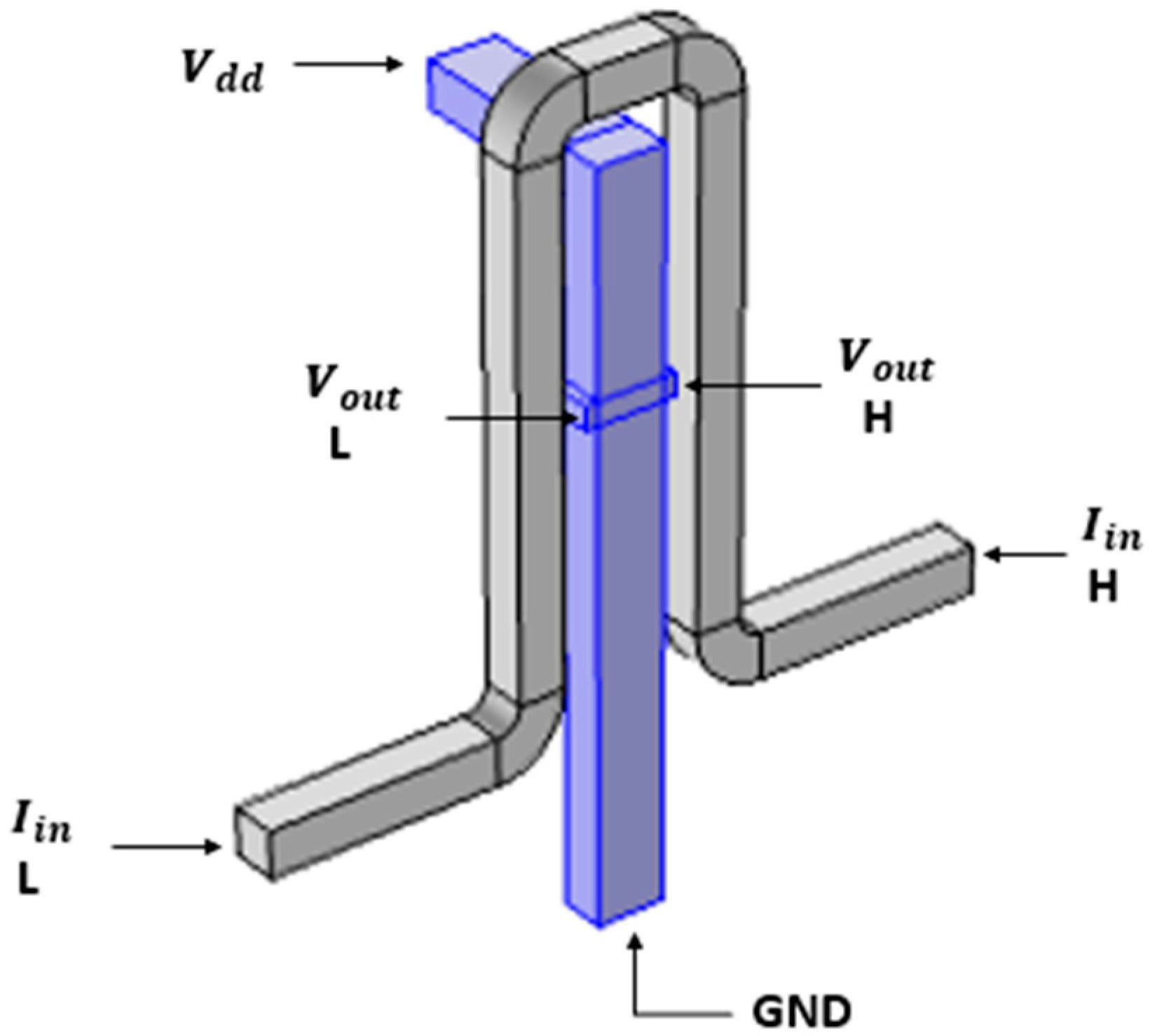
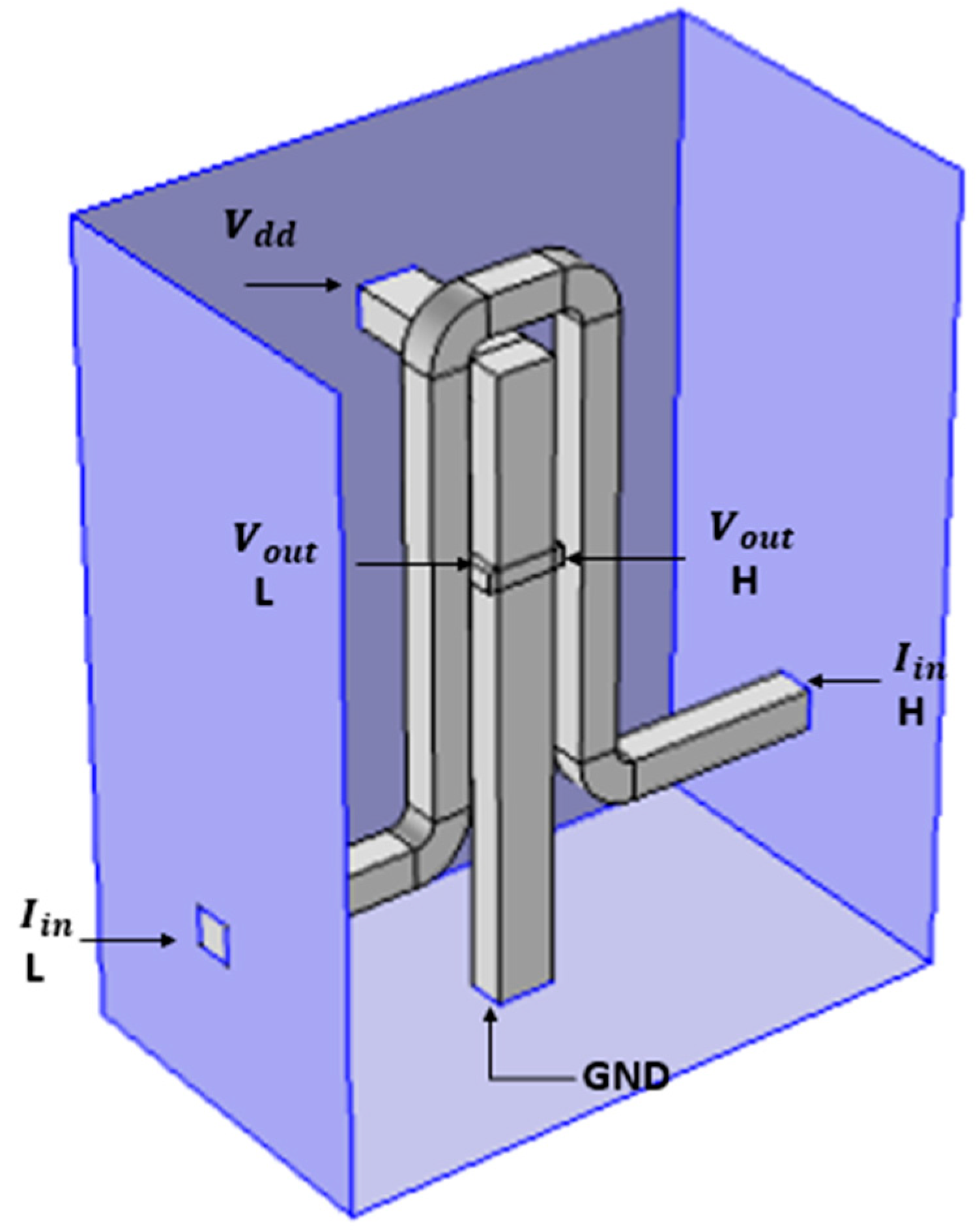
2. Device Structure
2.1. Nanoscale Device Concept and Advantages
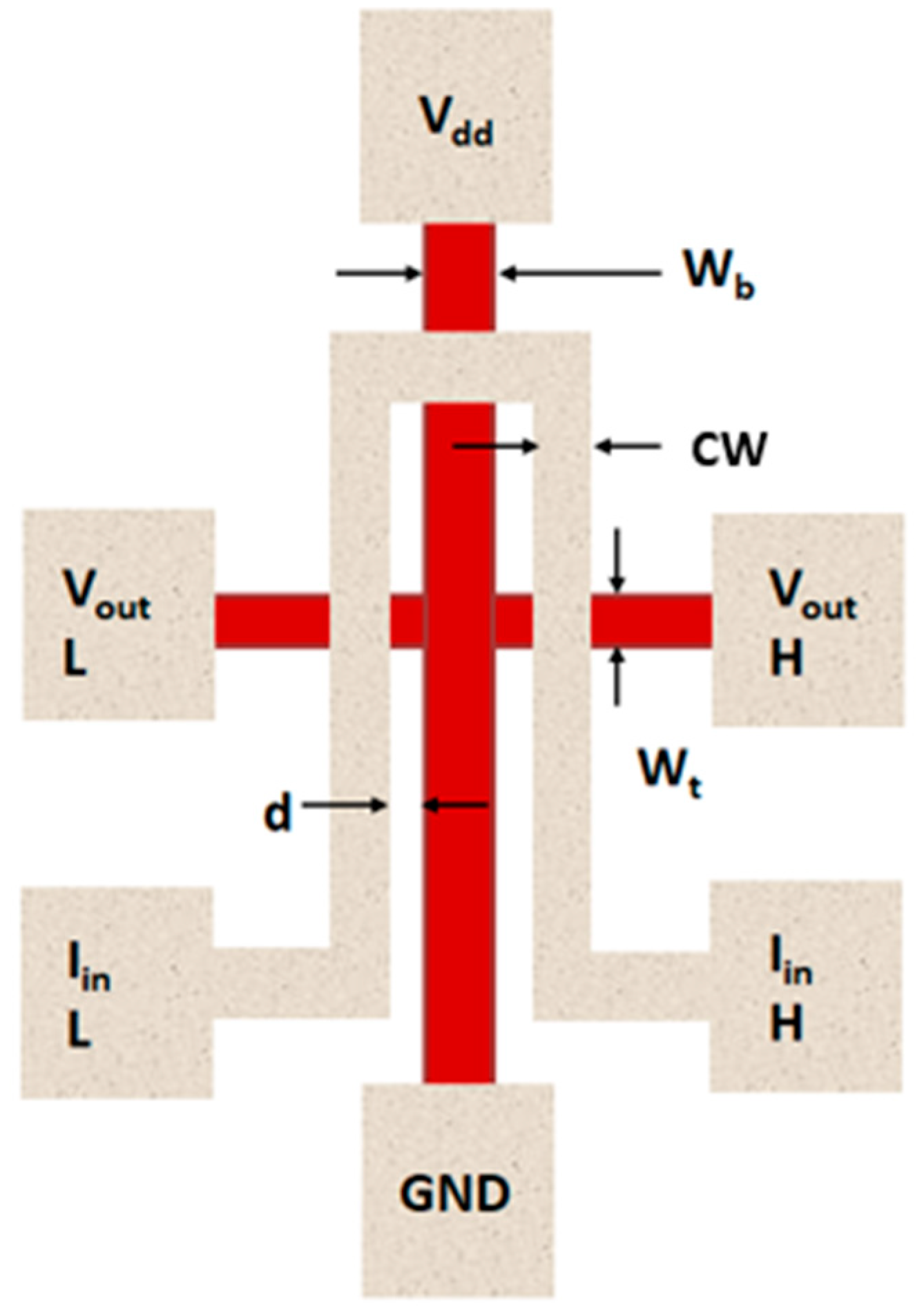
2.2. Device Architecture and Design
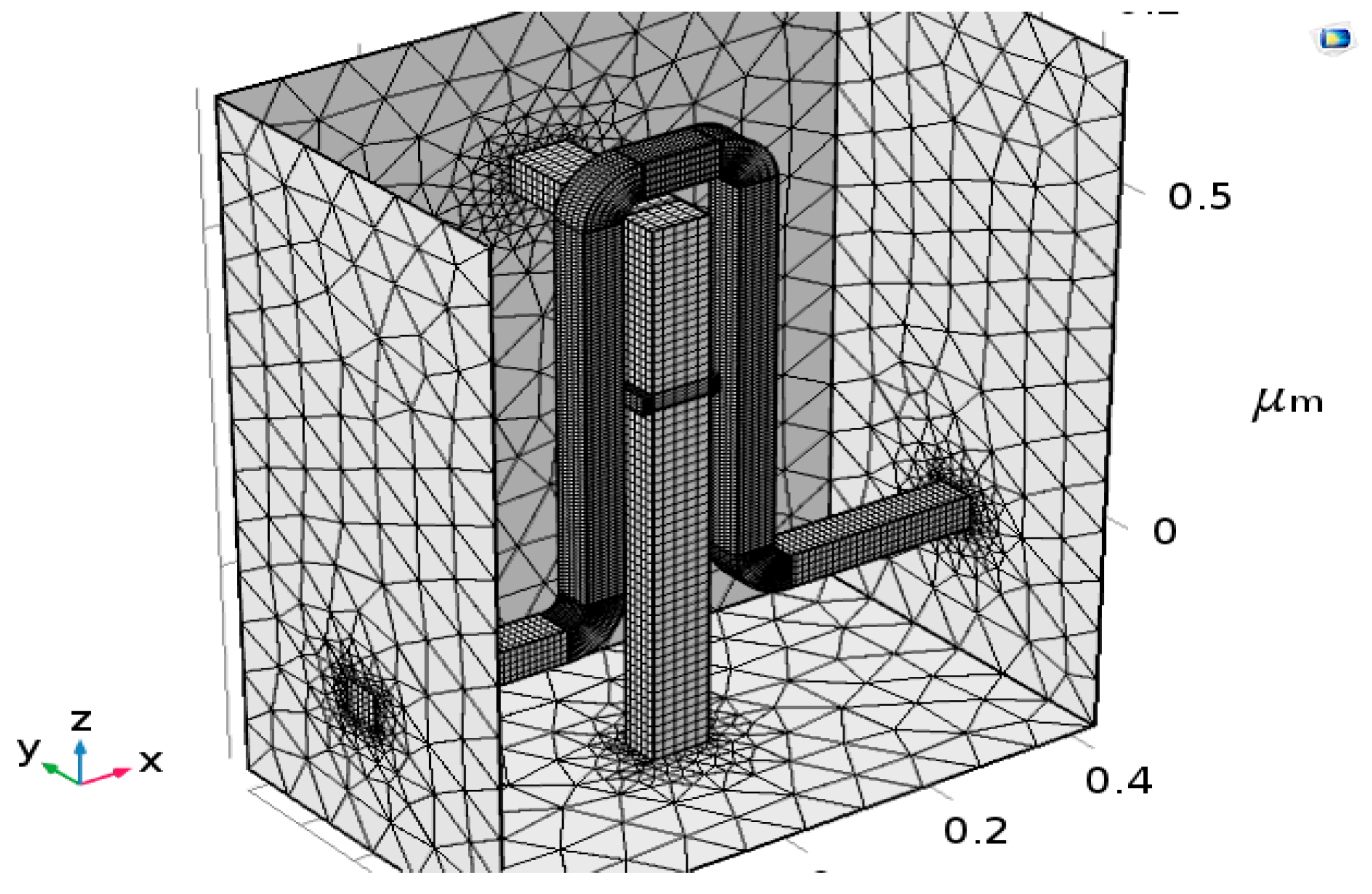
2.3. Simulation Considerations
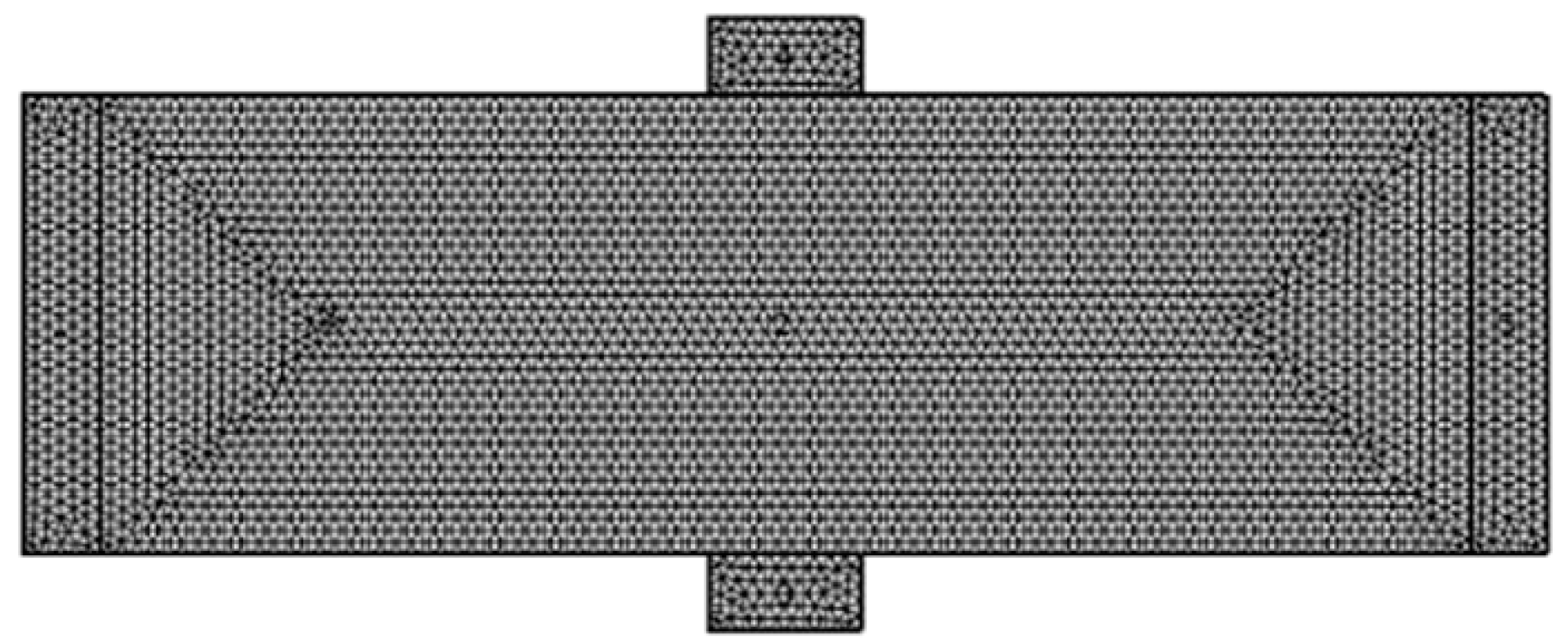
2.4. Mesh Accuracy and Considerations
3. Analytical Model
3.1. Classical Hall Effect
3.2. DC Hall Magneto-Resistance
3.3. Approximation to the Dynamic Magneto-Conductivity Tensor for Free Electrons
3.4. Heterodyne Hall Effect in a Two-Dimensional Electron Gas
3.5. Dielectric Tensor for Free Electron Model
4. Results
4.1. Parameters
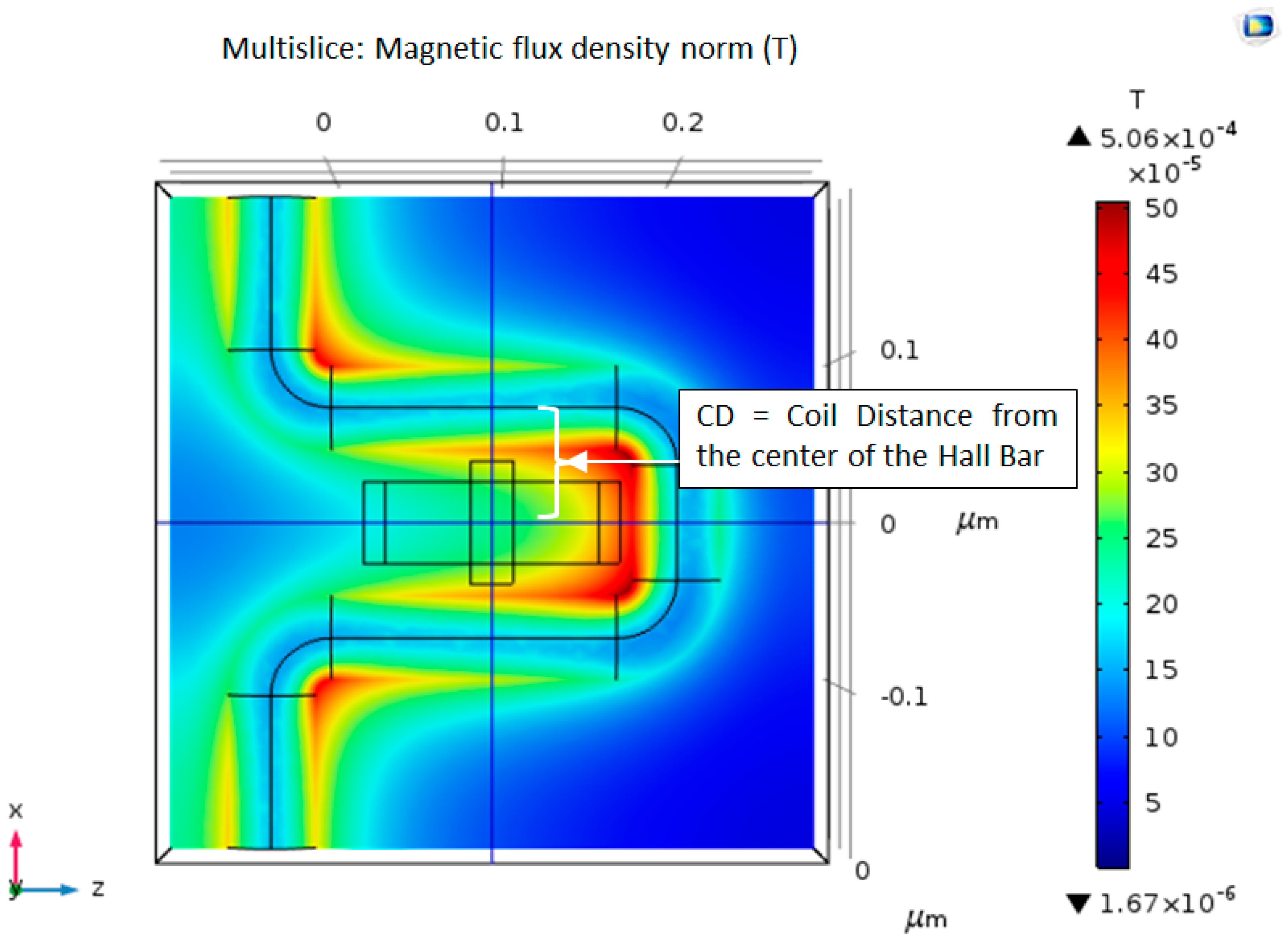
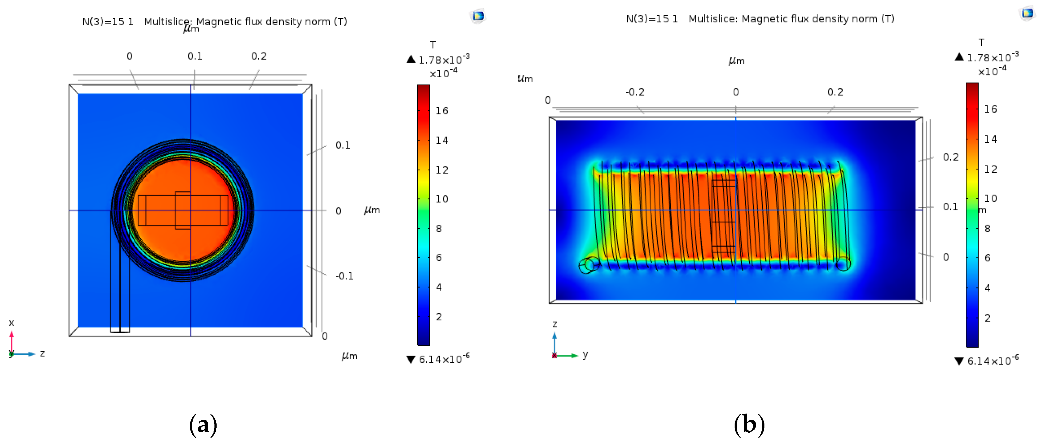
4.2. Single Loop Copper Wire Magnetic Field
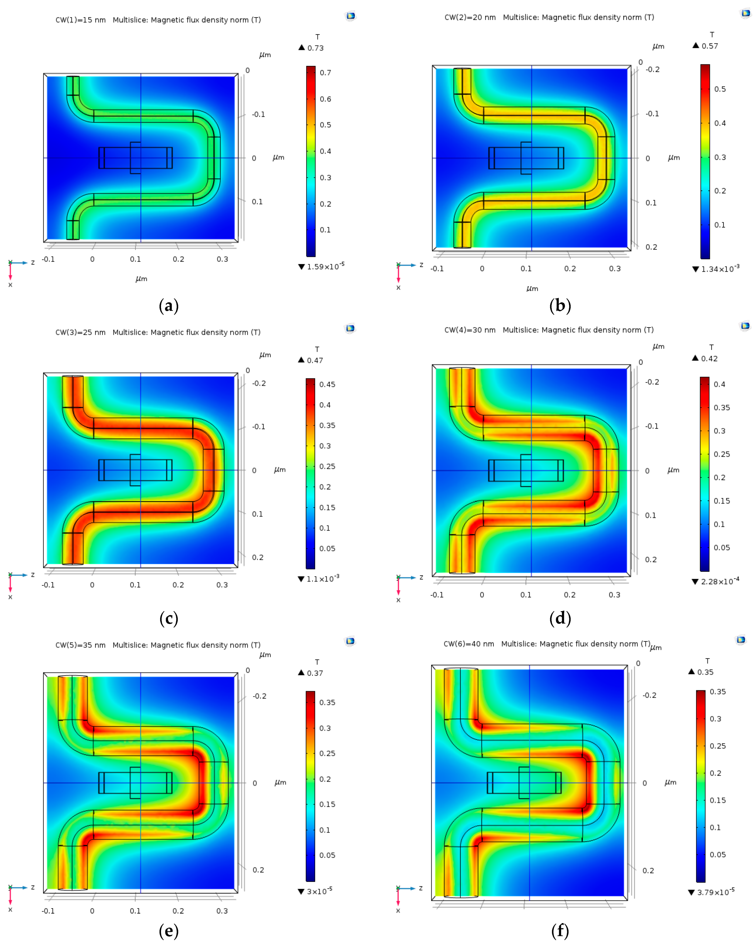
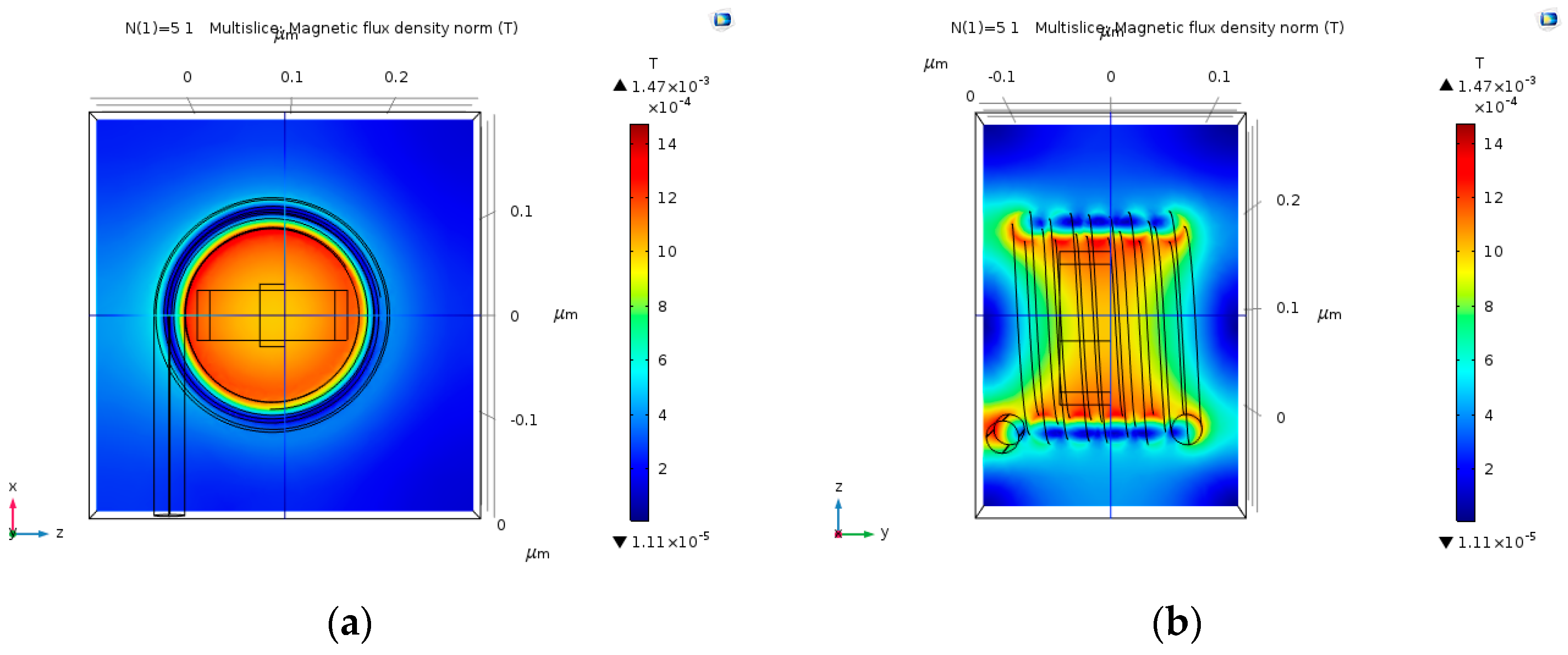
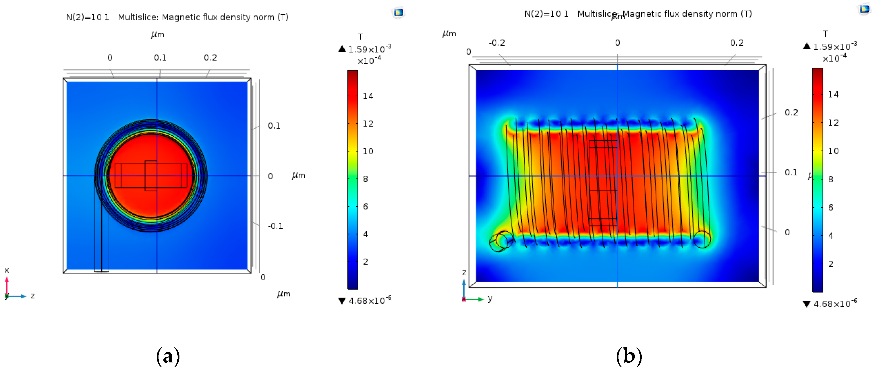
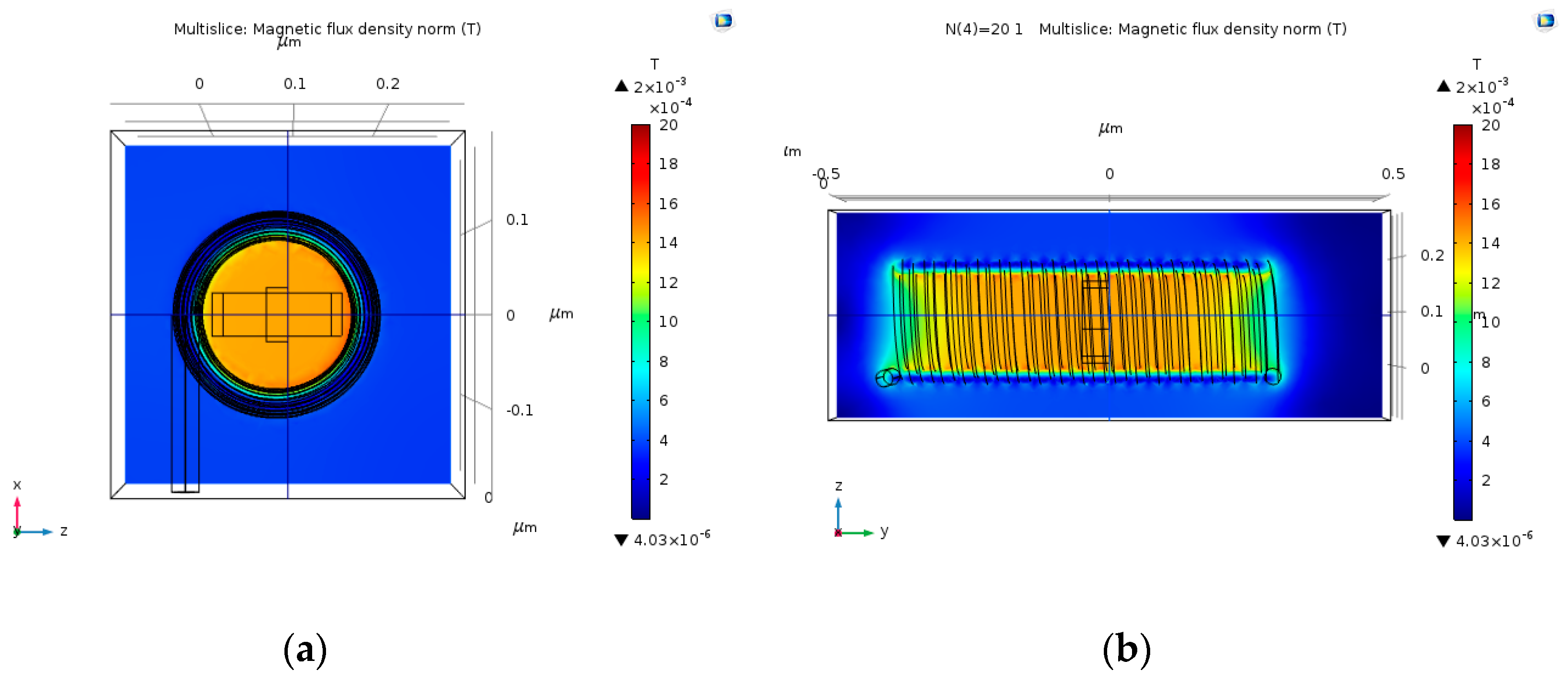
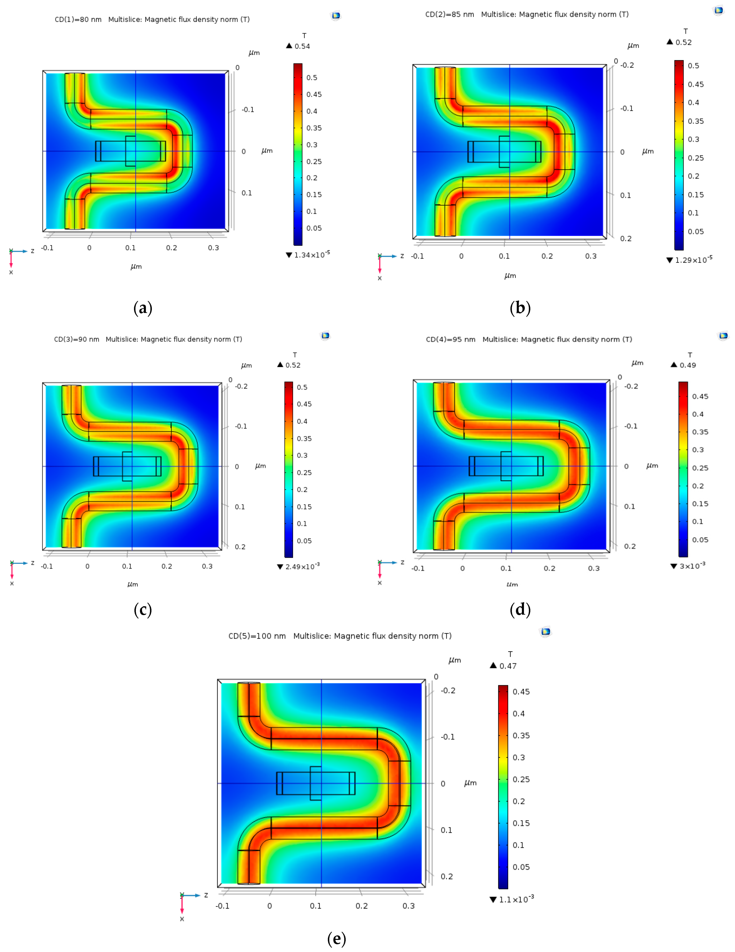
4.3. Multi-Loop Copper Wire Magnetic Field
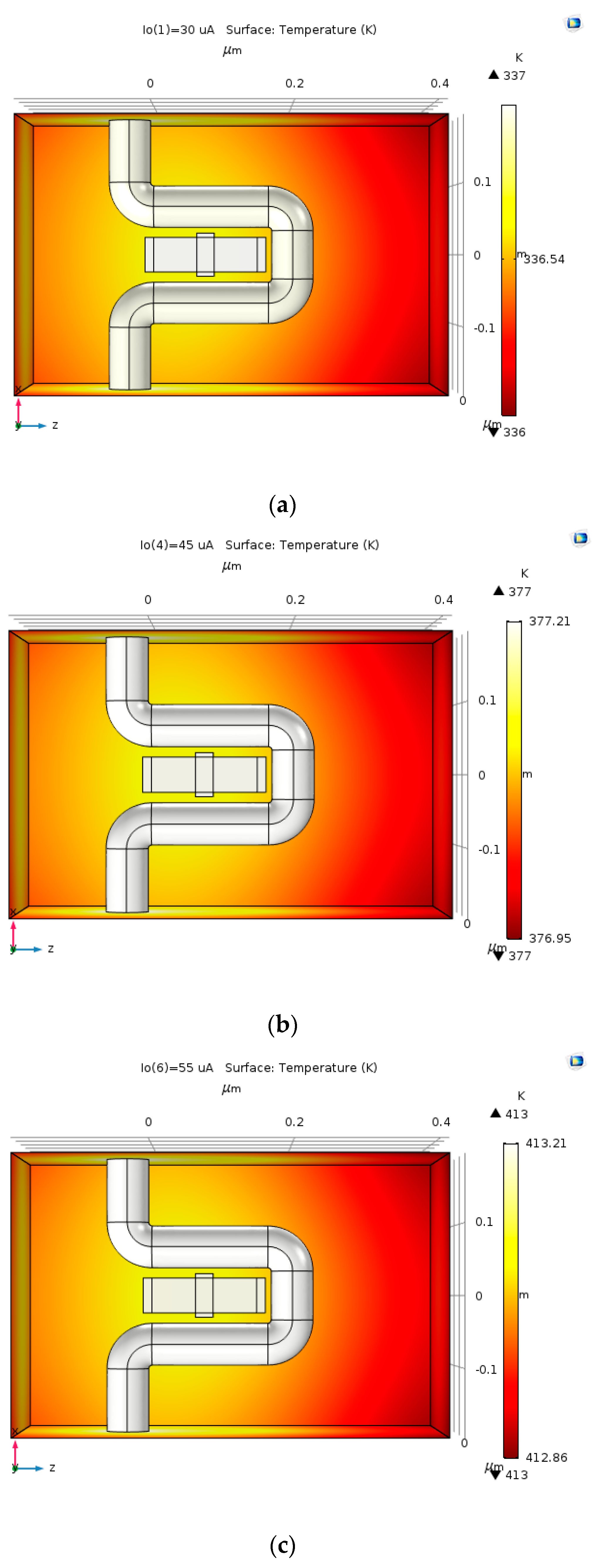
4.4. Heat Transfer of the Device
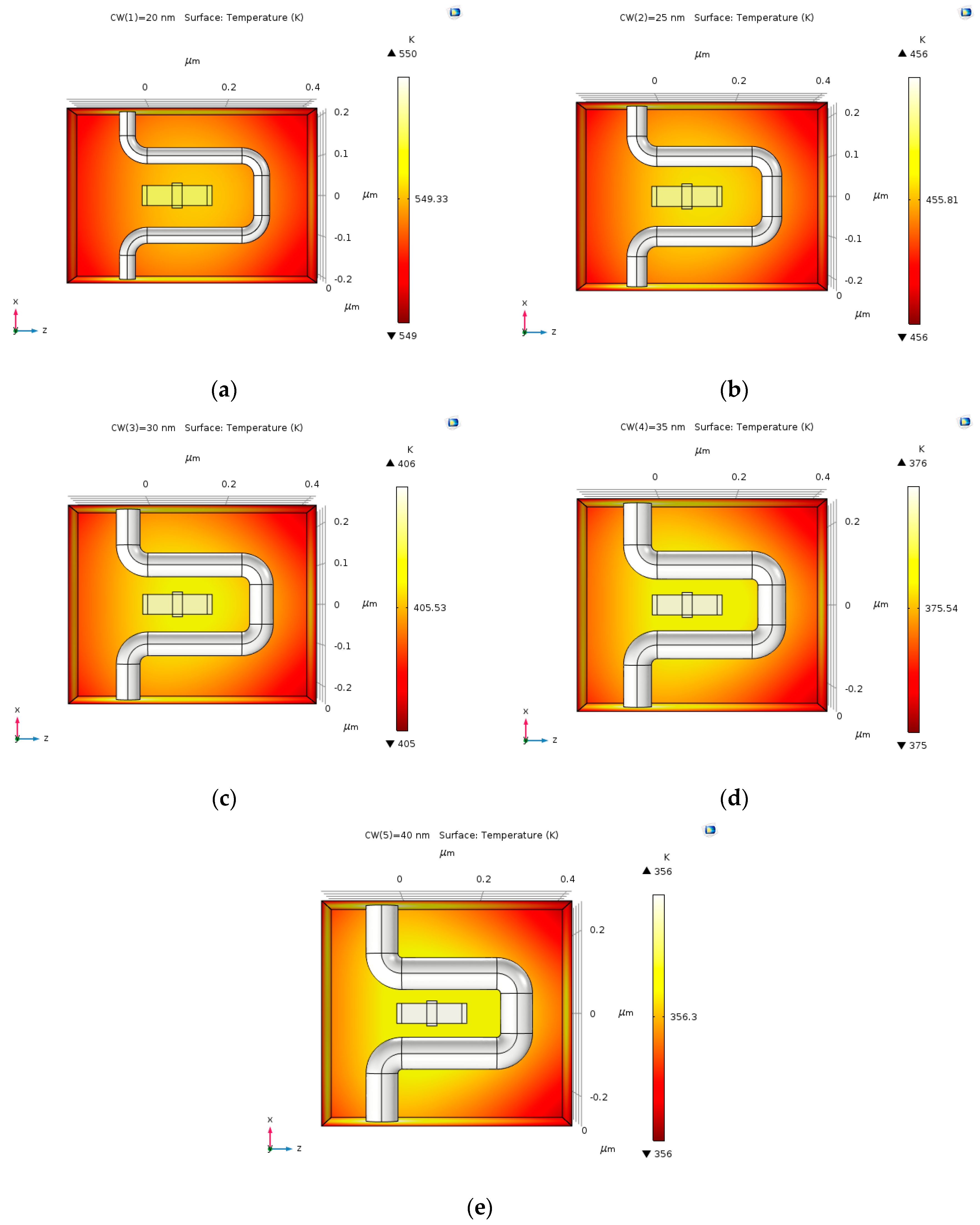
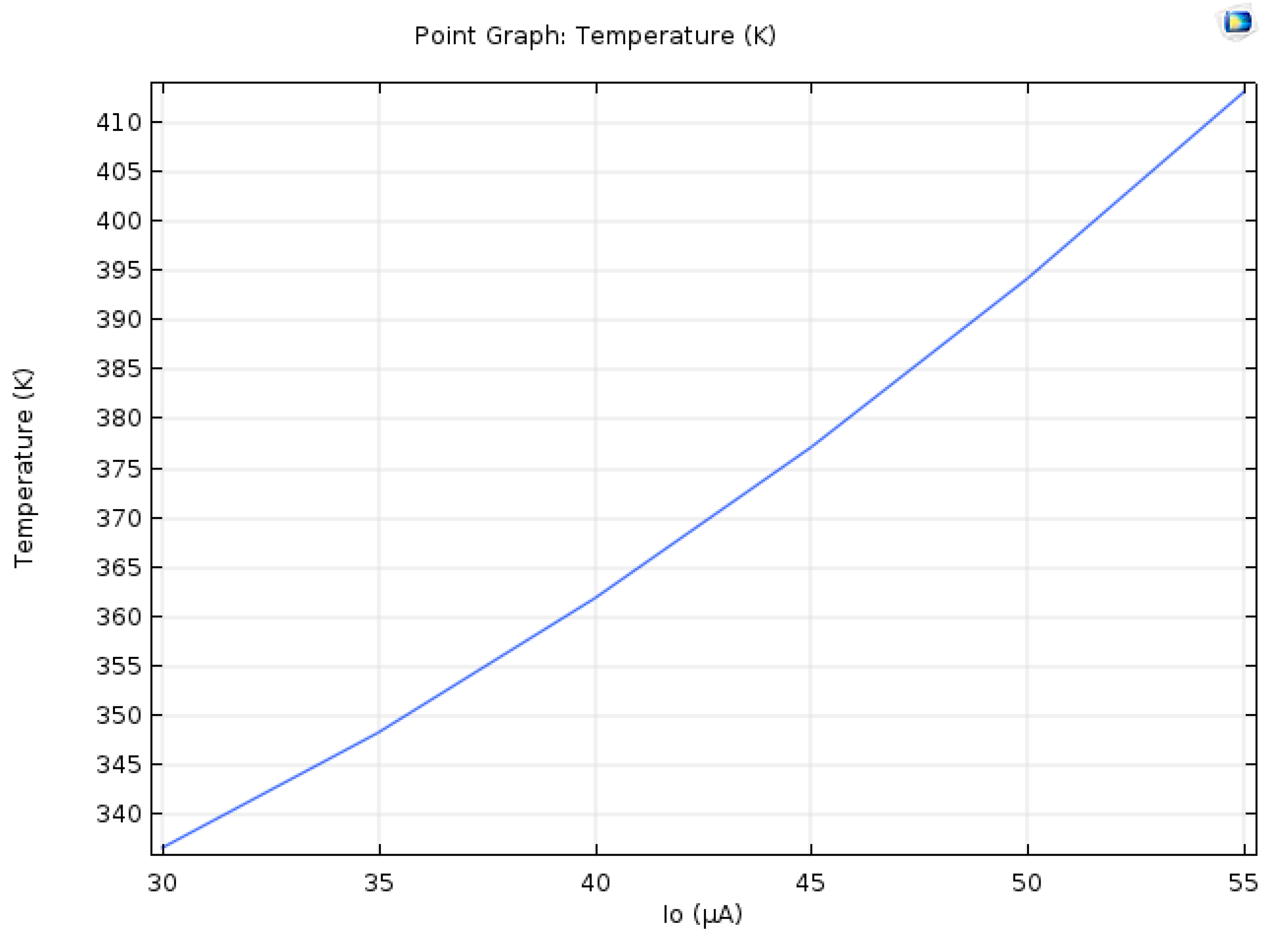
4.5. Current Density Effect on Joule Heating
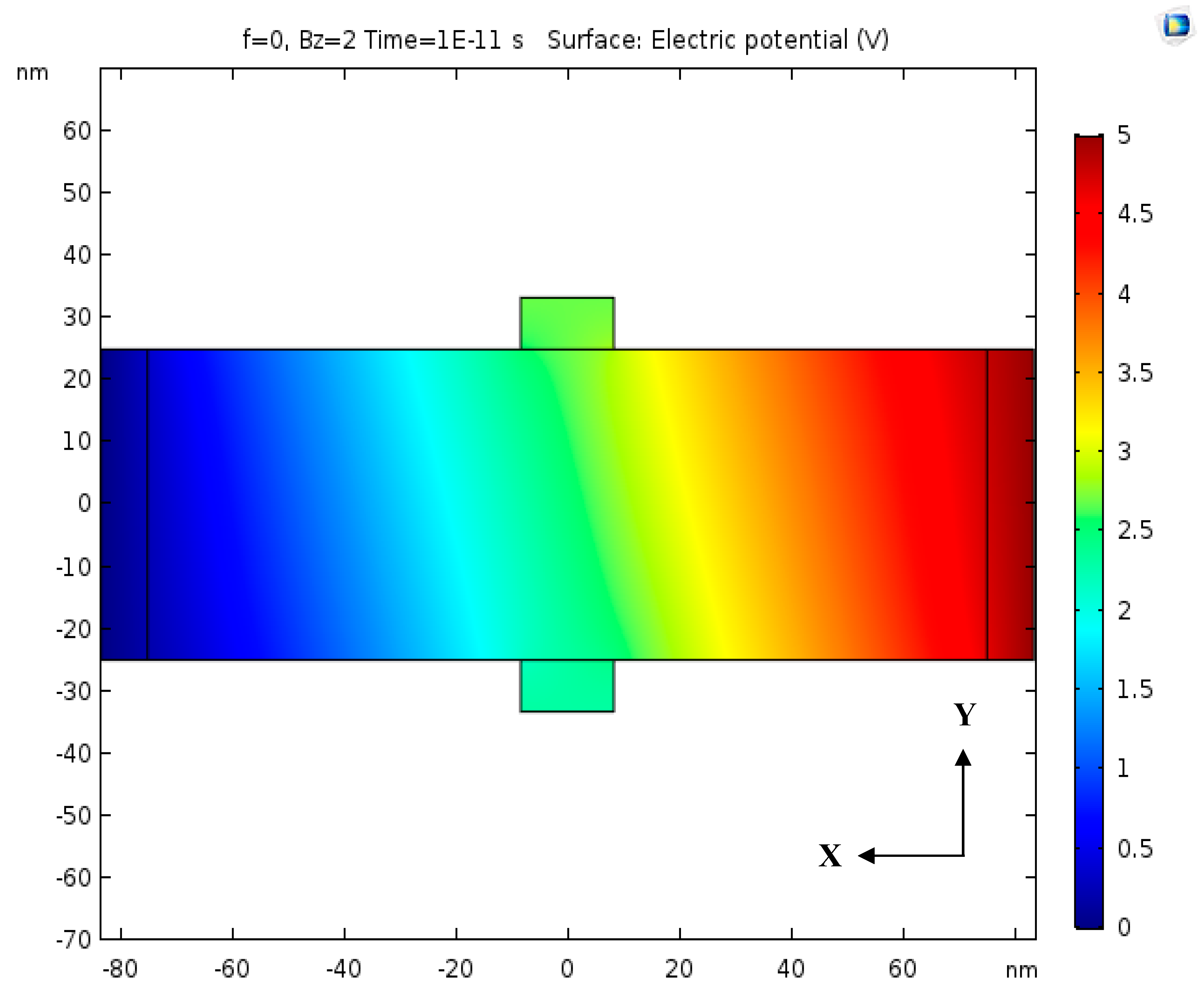
4.6. Hall Bar 2D AC/DC Simulations
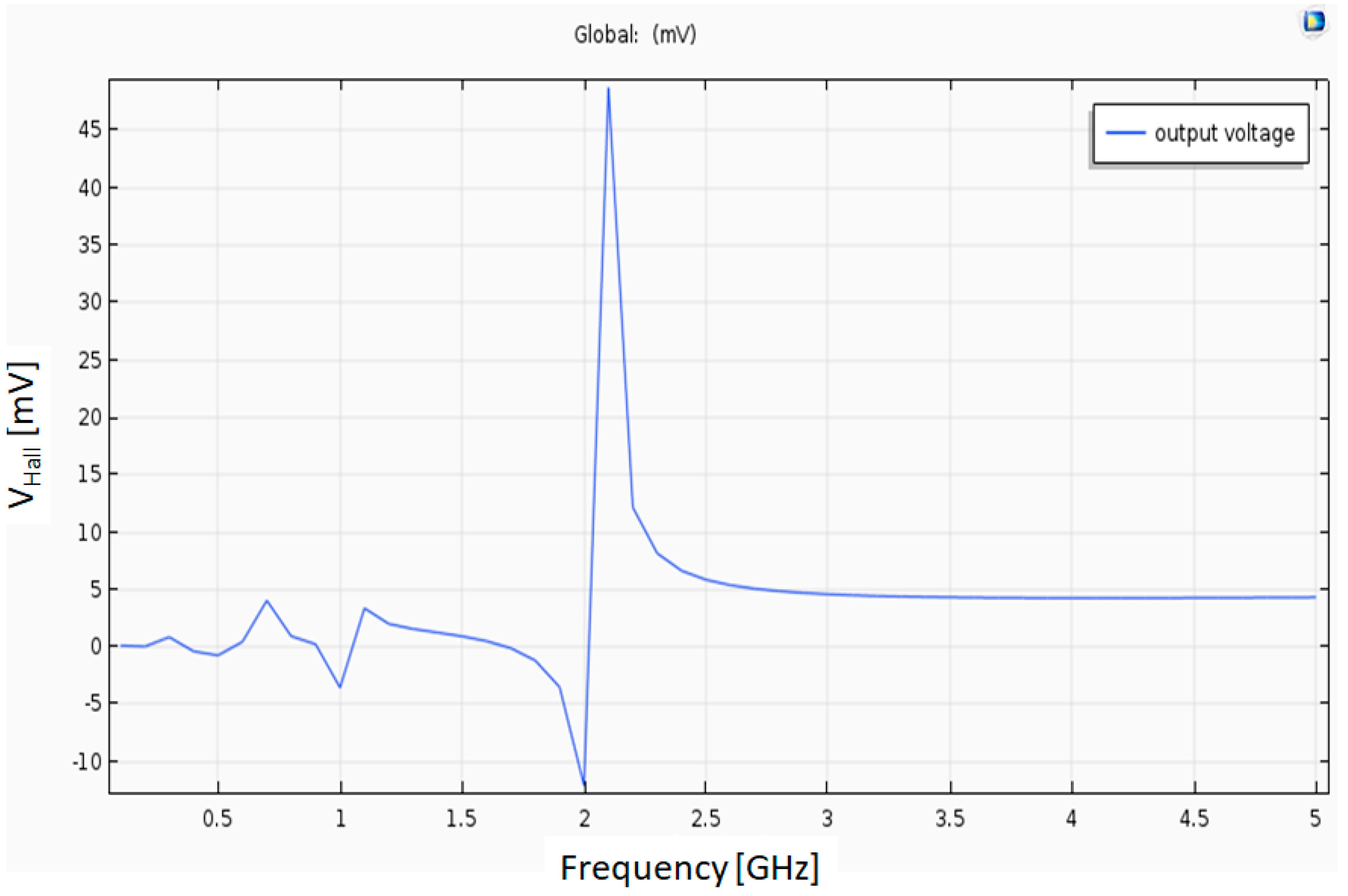
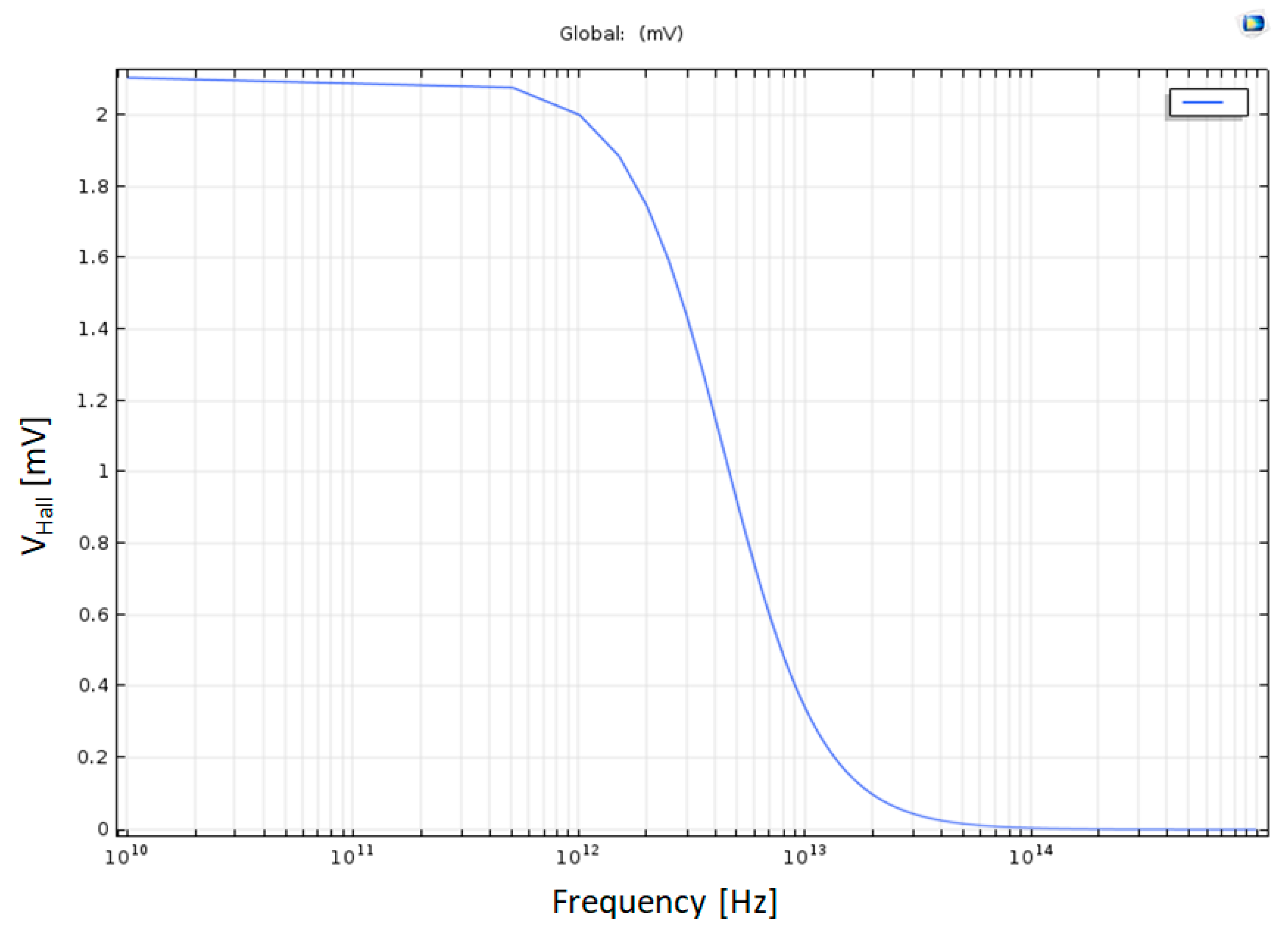
4.7. Frequency Effect on Hall Voltage
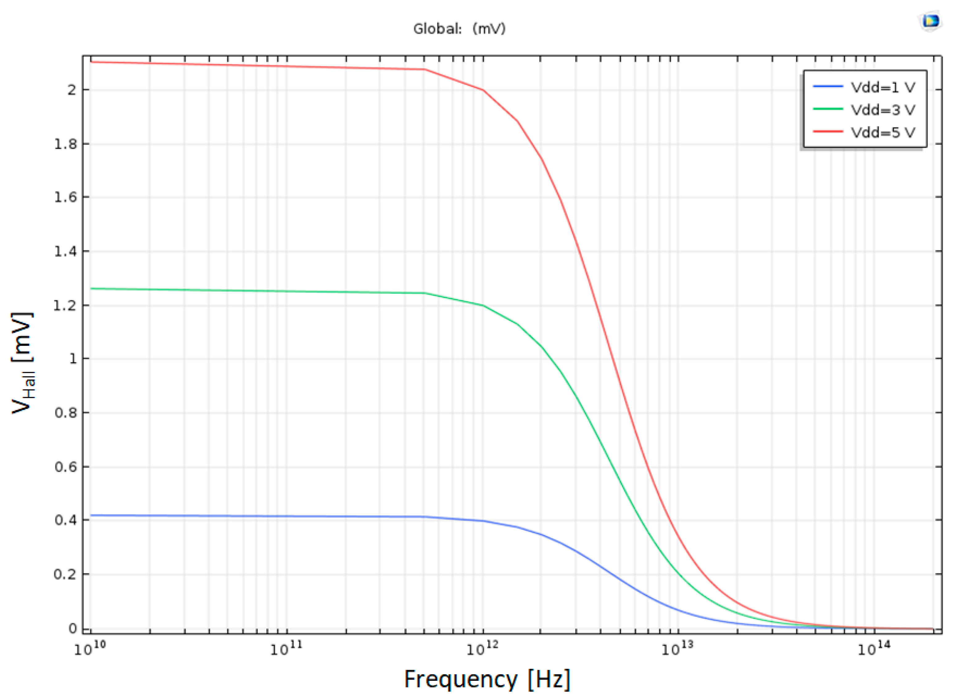
4.8. The Effect of the Applied Voltage Vdd on Hall Voltage
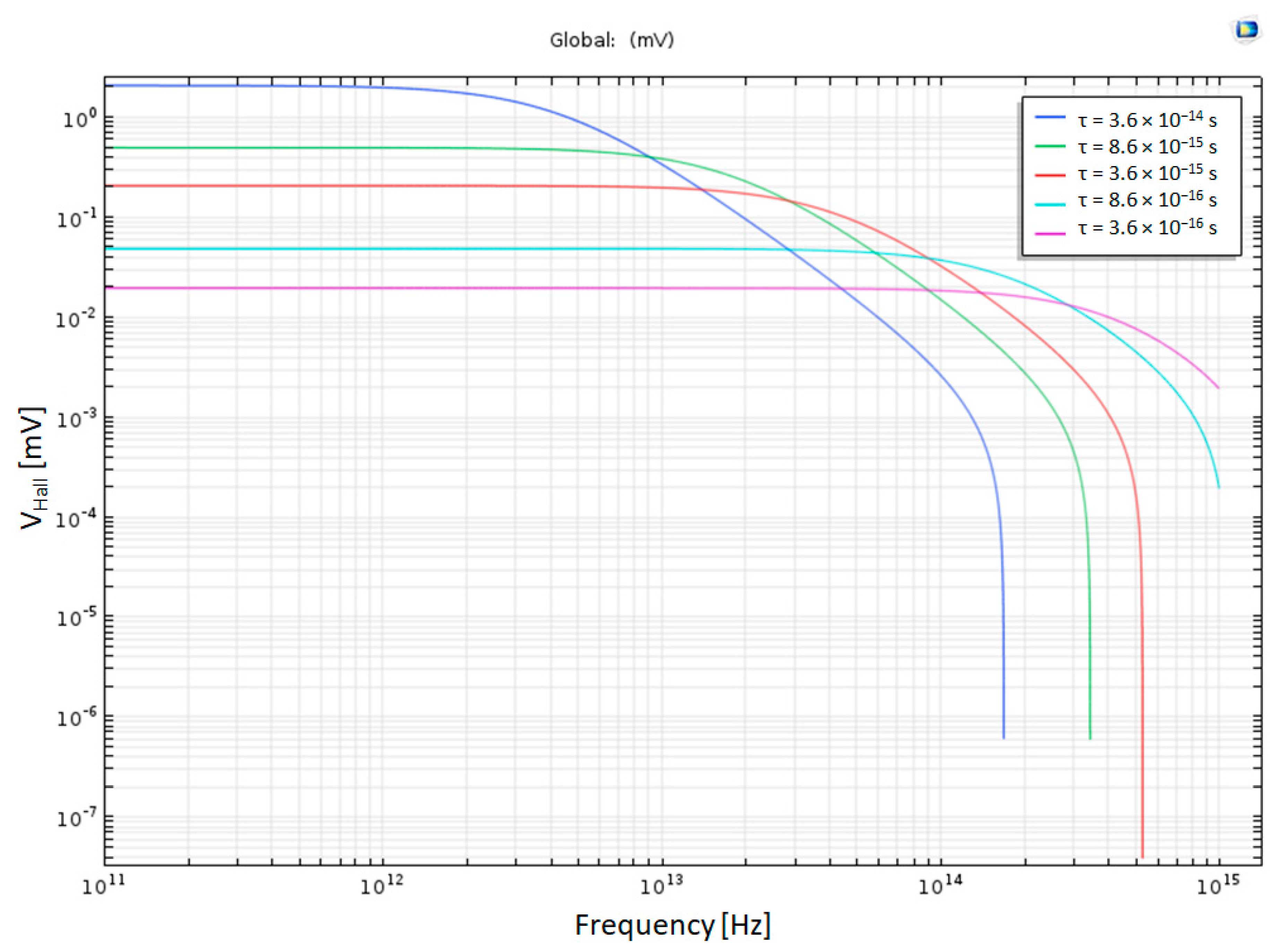
4.9. The Effects of Scattering Time on the Hall Voltage
4.10. Heterodyne Hall Effect Simulation
5. Discussion
5.1. Accuracy
5.2. High Temperature
- Optimization of the HAND size—as we increase the electromagnet cross-section area, the larger the sustained current, the stronger the magnetic field is. However, it is important to keep HAND small enough, first in order to prevent it from losing its nanoscale advantage. In such a case, the magnetic field in the Hall Bar zone may be even weaker.
- The use of different materials—different materials may sustain higher current densities than copper, therefore it could be part of the solution to the high temperature.
- The field of superconductors—superconductors may help in producing the magnetic field we need, this time with lower generated temperatures.
- Changing the geometry and components of the HAND—increasing the loop density, as shown above in the multi-loop simulation, might help in increasing the magnetic field intensity with the same current density. Moreover, adding a ferromagnetic core may be a possible solution in order to concentrate the magnetic flux and create a more powerful magnet.
6. Conclusions
7. Patents
Author Contributions
Funding
Acknowledgments
Conflicts of Interest
References
- Hall, E.H. On a new action of the magnet on electric currents. Am. J. Math. 1879, 2, 287–292. [Google Scholar] [CrossRef]
- Lorentz, H.A. On positive and negative electrons. Proc. Am. Philos. Soc. 1906, 183, 103–109. [Google Scholar]
- Mak, K.F.; McGill, K.L.; Park, J.; McEuen, P.L. The valley hall effect in MoS2 transistors. Science 2014, 344, 1489–1492. [Google Scholar] [CrossRef] [PubMed]
- Ramsden, E. Hall-Effect Sensors: Theory and Practice, 2nd ed.; Elsevier: New York, NY, USA, 2006. [Google Scholar]
- Diduck, Q.; Margala, M.; Feldman, M.J. A Terahertz Transistor Based on Geometrical Deflection of Ballistic Current. In Proceedings of the IEEE MTT-S 2006 International Microwave Symposium Digest, San Francisco, CA, USA, 11–16 November 2006; pp. 345–347. [Google Scholar]
- Sherwood, J. Radical Ballistic Computing Chip Bounces Electrons Like Billards. News of University of Rochester, 16 August 2006. [Google Scholar]
- Bell, T.E. The quest for ballistic action: Avoiding collisions during electron transport to increase switching speeds is the goal of the ultimate transistor. IEEE Spectr. 1986, 23, 36–38. [Google Scholar] [CrossRef]
- Natori, K. Ballistic metal-oxide semiconductor field effect transistor. J. Appl. Phys. 1994, 76, 4879–4890. [Google Scholar] [CrossRef]
- Ross, I.; Thompson, N. An Amplifier based on the Hall Effect. Nature 1955, 175, 1004. [Google Scholar] [CrossRef]
- Madelung, O.; Weiss, H. Die elektrischen Eigenschaften von Indiumantimonid II. Natureforsch 1954, 9, 527–534. [Google Scholar] [CrossRef]
- Saker, E.W.; Cunnell, F.A. Intermetallic Semiconductors. Research 1954, 7, 114–120. [Google Scholar]
- Karsenty, A.; Mandelbaum, Y. Computer algebra challenges in nanotechnology: Accurate modeling of nanoscale electro-optic devices using finite elements method. Math. Comput. Sci. 2019, 13, 117–130. [Google Scholar] [CrossRef]
- Karsenty, A.; Mandelbaum, Y. Computer algebra in nanotechnology: Modeling of nano electro-optic devices using finite element method (FEM). In Proceedings of the ACA 2017 23rd Conference on Applications of Computer Algebra, Session 6: Computer Algebra for Applied Physics, Jerusalem, Israel, 17–21 July 2017; p. 138. [Google Scholar]
- Comsol Multi-Physics Software Package Website. Available online: https://www.comsol.com/ (accessed on 25 September 2019).
- Matlab Software Package Website. MathWorks. Available online: https://www.mathworks.com/products/matlab.html. (accessed on 25 September 2019).
- Kittel, C. Introduction to Solid State Physics, 8th ed.; Wiley: New York, NY, USA, 1976; p. 153. [Google Scholar]
- Oka, T.; Bucciantini, L. Heterodyne hall effect in a two dimensional electron Gas. Phys. Rev. 2016, 94, 155133. [Google Scholar] [CrossRef]
- Sze, S.M. Physics of Semiconductor Devices, 2nd ed.; Wiley & Sons: Hoboken, NJ, USA, 1981. [Google Scholar]
- Convective Heat Transfer Coefficient Table Chart. Available online: https://www.engineersedge.com/heat_transfer/convective_heat_transfer_coefficients__13378.htm (accessed on 25 September 2019).
- Gall, D. Electron mean free path in elemental metals. J. Appl. Phys. 2016, 119, 085101. [Google Scholar] [CrossRef]
- Fan, Z.; Garcia, J.H.; Cummings, A.W.; Barrios, J.E.; Panhans, M.; Harju, A.; Roche, S. Linear scaling quantum transport methodologies. Rev. Mod. Phys. 2018, arXiv:1811.07387v1. [Google Scholar]
- Nazin, S.; Shikin, V. Ballistic transport under quantum Hall effect conditions. Phys. B Condens. Matter 2012, 407, 1901–1904. [Google Scholar] [CrossRef]
- Gooth, J.; Borg, M.; Schmid, H.; Bologna, N.; Rossell, M.D.; Wirths, S.; Riel, H. Transition to the quantum hall regime in InAs nanowire cross-junctions. Semicond. Sci. Technol. 2019, 34, 035028. [Google Scholar] [CrossRef]
- Nikolajsen, J.R. Edge States and Contacts in the Quantum Hall Effect. Bachelor’s Thesis, University of Copenhagen, Copenhagen, Denmark, 12 June 2013. [Google Scholar]


| Parameter | Parameters Definition | Values |
|---|---|---|
| Device Parameters: | ||
| σ2D Cu | Hall Bar Conductivity in 2D simulations | 5.998 × 10⁷ S/m |
| Σ Doped Si | Hall Bar Conductivity in heterodyne simulation | 1.04 × 10³ S/m |
| RH | Hall Coefficient | 8.1202 × 10¹¹ m3/(sA) |
| WB | Hall Bar Width | 50 nm |
| HB | Hall Bar length | 150 nm |
| TB | Hall Bar Thickness | 50 nm |
| µe Cu | Electron Mobility in Copper | 48.705 cm2/(V |
| µe Si | Electron Mobility in Silicon | 1400 cm2/(V [18] |
| µe GaAs | Electron Mobility in Gallium Arsenide | 8500 cm2/(V [18] |
| Comsol Setup Used Parameters: | ||
| Bz | Magnetic field in Z direction | 0.3 T |
| Τ | Scattering Time of Copper | 3.6 × 10⁻¹⁴ s |
| τT | A variable to change the scattering time | 3.6 × 10⁻¹⁴ s–3.6 × 10⁻¹⁶ s |
| Freq | Frequency | |
| τ | Scattering time of silicon | 0.21 × 10⁻¹² s |
| Vdd | Applied Voltage | 1 V–5 V |
| I0 | Input electric current in the Joule heating simulation | 30 µA–55 µA |
| Measured Parameters: | ||
| |VHall 2D| | Output Voltage in 2D AC/DC simulations | 2.1 mV |
| fc.o. Cu | Cut off frequency in Copper | ~1 THz |
| B | Magnetic flux density norm | Depends on simulation |
| T | Temperature | Depends on simulation |
| VHall Het | Resonant Output voltage in the heterodyne simulation | 45 V |
© 2019 by the authors. Licensee MDPI, Basel, Switzerland. This article is an open access article distributed under the terms and conditions of the Creative Commons Attribution (CC BY) license (http://creativecommons.org/licenses/by/4.0/).
Share and Cite
Karsenty, A.; Mottes, R. Hall Amplifier Nanoscale Device (HAND): Modeling, Simulations and Feasibility Analysis for THz Sensor. Nanomaterials 2019, 9, 1618. https://doi.org/10.3390/nano9111618
Karsenty A, Mottes R. Hall Amplifier Nanoscale Device (HAND): Modeling, Simulations and Feasibility Analysis for THz Sensor. Nanomaterials. 2019; 9(11):1618. https://doi.org/10.3390/nano9111618
Chicago/Turabian StyleKarsenty, Avi, and Raz Mottes. 2019. "Hall Amplifier Nanoscale Device (HAND): Modeling, Simulations and Feasibility Analysis for THz Sensor" Nanomaterials 9, no. 11: 1618. https://doi.org/10.3390/nano9111618
APA StyleKarsenty, A., & Mottes, R. (2019). Hall Amplifier Nanoscale Device (HAND): Modeling, Simulations and Feasibility Analysis for THz Sensor. Nanomaterials, 9(11), 1618. https://doi.org/10.3390/nano9111618