Article

Fabrication of Ag and Mn Co-Doped Cu2ZnSnS4 Thin Film

School of Materials and Energy, Guangdong University of Technology, Guangzhou 510006, China
*
Author to whom correspondence should be addressed.
Nanomaterials 2019, 9(11), 1520; https://doi.org/10.3390/nano9111520
Submission received: 30 September 2019 / Revised: 17 October 2019 / Accepted: 23 October 2019 / Published: 25 October 2019

Abstract

:
Ag and Mn dopants were incorporated into Cu2ZnSnS4 thin film to reduce defects in thin film and improve thin film properties. Sol–gel and spin-coating techniques were employed to deposit Ag and Mn co-doped Cu2ZnSnS4 thin films. The structures, compositions, morphologies, and optical properties of the co-doped thin films were characterized. The experimental results indicate the formation of kesterite structure without Ag and Mn secondary phases. The amount of Ag in the thin films is close to that in the sols. The co-doped Cu2ZnSnS4 thin films have an absorption coefficient of larger than 1.3 × 104 cm−1, a direct optical band gap of 1.54–2.14 eV, and enhanced photoluminescence. The nonradiative recombination in Cu2ZnSnS4 thin film is reduced by Ag and Mn co-doping. The experimental results show that Ag and Mn incorporation can improve the properties of Cu2ZnSnS4 thin film.

1. Introduction

In recent years, the quaternary semiconducting Cu2ZnSnS4 has been recognized as a candidate to replace Cu(In,Ga)Se2 absorber due to its promising optical and electronic properties and its earth-abundant and non-toxic component elements [1,2]. The absorption coefficient of Cu2ZnSnS4 in the visible region is larger than 1 × 104 cm−1. The direct band gap of Cu2ZnSnS4 is around 1.50 eV, which matches with the suitable value for absorber application in solar cells [3,4].
The record conversion efficiencies of Cu2ZnSnS4 and Cu2ZnSn(S,Se)4 thin-film solar cells are 11.0% [5] and 12.6% [6], respectively, which are still lower than that of competitive Cu(In,Ga)Se2 thin-film solar cell. Further improvement is necessary for Cu2ZnSnS4-based thin-film solar cell. The low efficiency of Cu2ZnSnS4 thin-film solar cell is attributed to the poor crystallinity of Cu2ZnSnS4, easy formation of secondary phases in Cu2ZnSnS4, defect states in Cu2ZnSnS4 and heterojunction interface, unfavorable band alignment at the buffer/absorber and absorber/back electrode interfaces, etc. [7].
Cation substitution is a useful method to enhance the properties of Cu2ZnSnS4 thin film and solar cell. The Cu+, Zn2+, and Sn4+ ions in Cu2ZnSnS4 can be substituted by extrinsic ions. Ag doping can occupy the Cu site in the Cu2ZnSnS4 lattice to reduce the harmful CuZn anti-site and VCu defects because the formation energy of AgZn defect is higher than that of CuZn defect [8,9,10,11]. In addition, the band gap of Cu2ZnSnS4 can be adjusted by Ag doping [12,13].
The full or partial substitution of Zn by Cd, Fe, Mn, Mg, or Co has also been reported to increase the absorption of Cu2ZnSnS4, reduce the CuZn anti-site defect and ZnS secondary phase, and enhance the crystallinity of Cu2ZnSnS4 and conversion efficiency of Cu2ZnSnS4 thin-film solar cell [14,15,16,17,18]. The efficiency of Cd-doped Cu2ZnSnS4 solar cell has exceeded 11% [16].
Up to now, most of reports about cation substitution of Cu2ZnSnS4 have utilized single doping, that is, only one dopant is used for substitution. Although the single substitution has demonstrated beneficial effects on Cu2ZnSnS4, there are still some issues. Ag substitution increases the band gap of Cu2ZnSnS4, leading to reduced wavelength of the absorption edge of Cu2ZnSnS4. The effect of reduced defects by Zn site substitution is limited. The optimum substitution ratio of single doping is in a narrow range. It needs precise composition regulation during thin film preparation. Compared with single doping, if different cations dope in Cu2ZnSnS4 to substitute different sites with different mechanisms, this is expected to further improve the properties of Cu2ZnSnS4 thin film. To the best of our knowledge, there is only one report about Ag and Cd co-doped Cu2ZnSnS4 [19]. However, Cd is a toxic element.
In this work, Cu2ZnSnS4 thin films were co-doped by Ag and Mn dopants using sol–gel and spin-coating methods. The Ag and Mn atoms substitute the Cu and Zn sites, respectively. Ag is commonly used for Cu substitution in Cu2ZnSnS4. Mn is earth-abundant and non-toxic. The sol–gel process has an advantage in thin film doping because the chemical homogeneity of sol can reach molecular or even atomic level. The structural, compositional, morphological, and optical properties of Ag and Mn co-doped Cu2ZnSnS4 thin films were characterized.

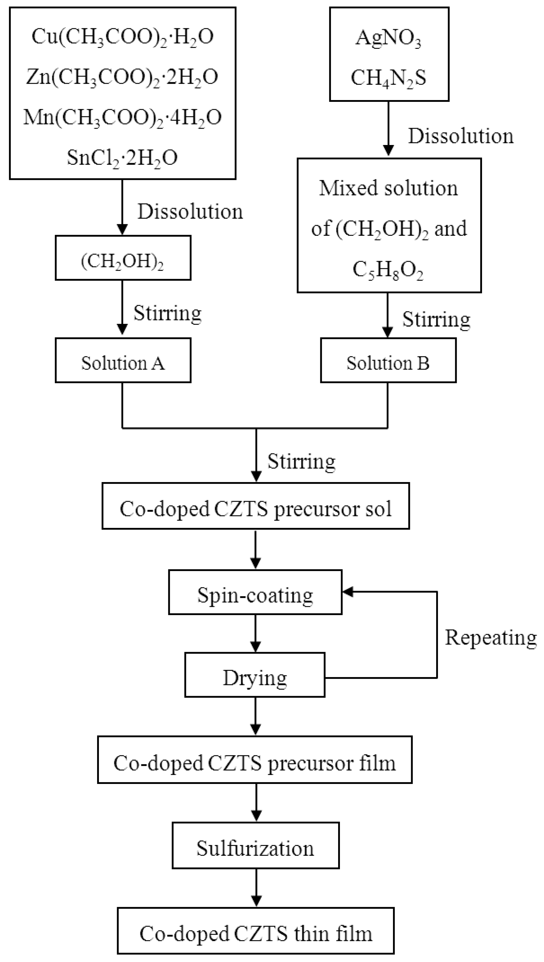
2. Materials and Methods

Figure 1 illustrates the fabrication process of Ag and Mn co-doped Cu2ZnSnS4 thin films. Cu(CH3COO)2·H2O, Zn(CH3COO)2·2H2O, SnCl2·2H2O, CH4N2S, and C5H8O2 were purchased from Shanghai Aladdin Bio-Chem Technology Co., LTD, Shanghai, China; Mn(CH3COO)2·4H2O, (CH2OH)2, and AgNO3 were purchased from Guangzhou Chemical Reagent Factory, Guangzhou, China, Sinopharm Chemical Reagent Co., Ltd., Shanghai, China, and Guangdong Guanghua Sci-Tech Co., Ltd., Shantou, China, respectively. Cu(CH3COO)2·H2O, Zn(CH3COO)2·2H2O, Mn(CH3COO)2·4H2O, and SnCl2·2H2O were sequentially dissolved in an organic (CH2OH)2 solvent, and then stirred at 60 °C for 2 h to obtain a milky solution, which was labeled as solution A. AgNO3 and CH4N2S were added into a mixed solution of (CH2OH)2 and C5H8O2 (the volume ratio of (CH2OH)2 to C5H8O2 was 5:1). After stirring for 2 h at 60 °C, a homogeneous yellow solution labeled as solution B was formed. Then, solution A was added into solution B and stirred at 60 °C for 15 min to obtain a homogeneous precursor sol. The sol samples with different Ag amounts were prepared with atomic ratios of Ag/(Ag + Cu) = 0, 1/3, 2/3, and 1, Mn/(Mn + Zn) = 1/3, (Ag + Cu)/(Mn + Zn + Sn) = 0.85, (Mn + Zn)/Sn = 1.15, and S/(Ag + Cu) = 4. The prepared sols were aged for 96 h at atmospheric pressure without heating. After that, the sols were spin-coated onto FTO (fluorine-doped tin oxide)-coated glass substrates to fabricate Cu2ZnSnS4 precursor films. The spin-coating was performed at a rotation speed of 800 rpm for 20 s and then 3500 rpm for 35 s. The films were then dried on a hot plate at 250 °C for 4 min to remove residual organics. The coating and drying were repeated 10 times. Finally, the Cu2ZnSnS4 precursor films were sulfurized to obtain the final co-doped Cu2ZnSnS4 thin films. The precursor films and 1 g sulfur powders were putted in a quartz boat which was placed in the center of a tube furnace. The sulfurization was performed in a N2 + S atmosphere; the sulfurization temperature and sulfurization time were 530 °C and 60 min, respectively.
The structures of prepared thin films were measured by X-ray diffractometer (XRD, D/MAX-Ultima IV, Rigaku, Tokyo, Japan) using Cu-kα radiation with a wavelength of 0.154 nm). A Raman scattering spectrometer (FEX, NOST Company Limited, Seongnam, Korea) was used for better detection of phase structure in the thin film. The excitation wavelength of Raman measurement was 532 nm. A field emission scanning electron microscope (FESEM, SU8010, Hitachi, Tokyo, Japan) was used to observe the surface and cross-section morphologies of the co-doped Cu2ZnSnS4 thin films. The atomic ratios of thin films were measured by energy dispersive spectroscopy (EDS, SDD3030, IXRF Systems, Austin, TX, USA) which was attached to FESEM. The reflectance and transmittance of thin films were identified by a UV-Vis spectrophotometer (UV-3600 Plus, Shimadzu, Kyoto, Japan and TU1810, Pgeneral, Beijing, China). The photoluminescence (PL) properties of Cu2ZnSnS4 were measured by a fluorescence spectrophotometer (Fluorolog-3, HORIBA Instruments Incorporate, Irvine, CA, USA).

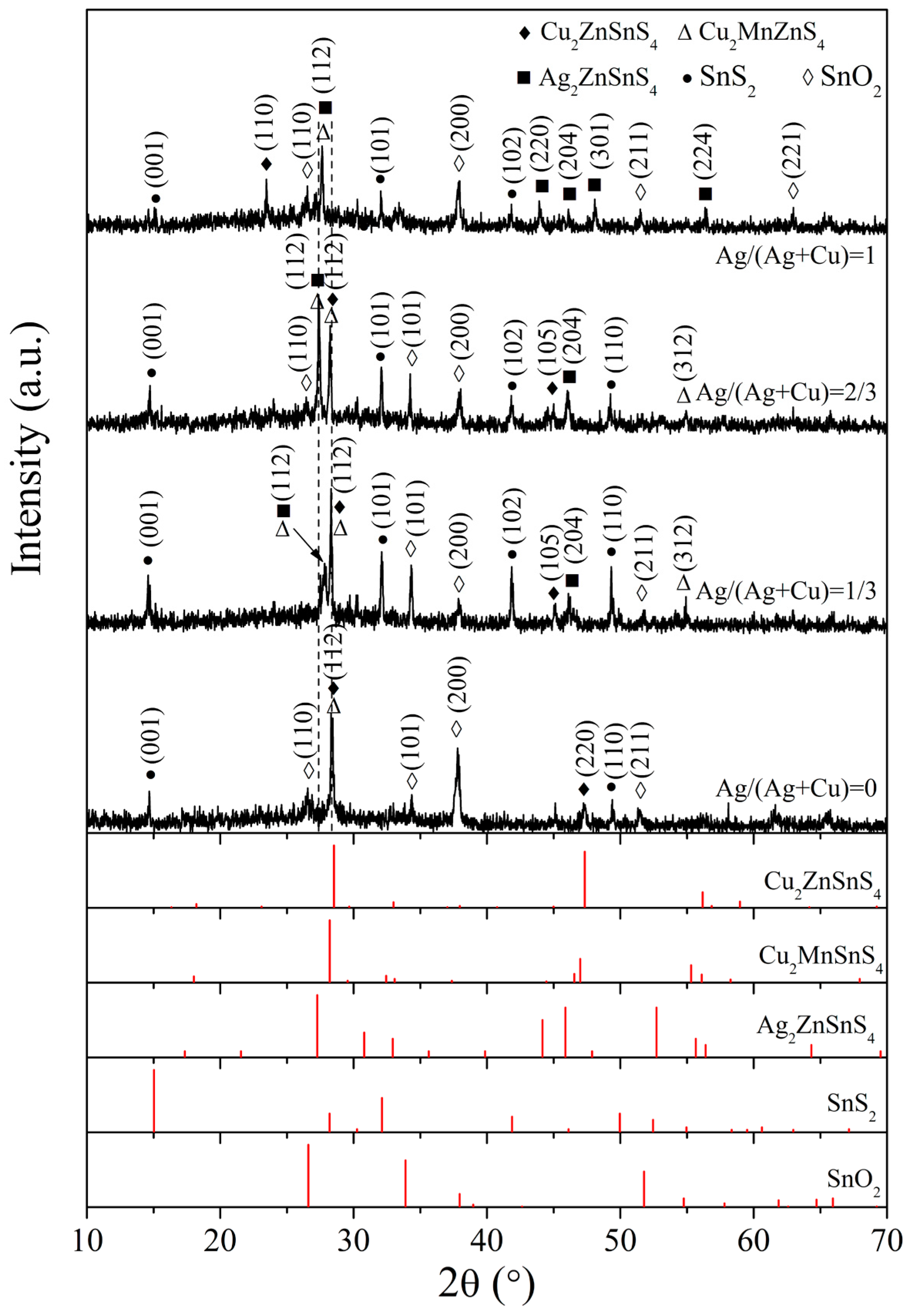
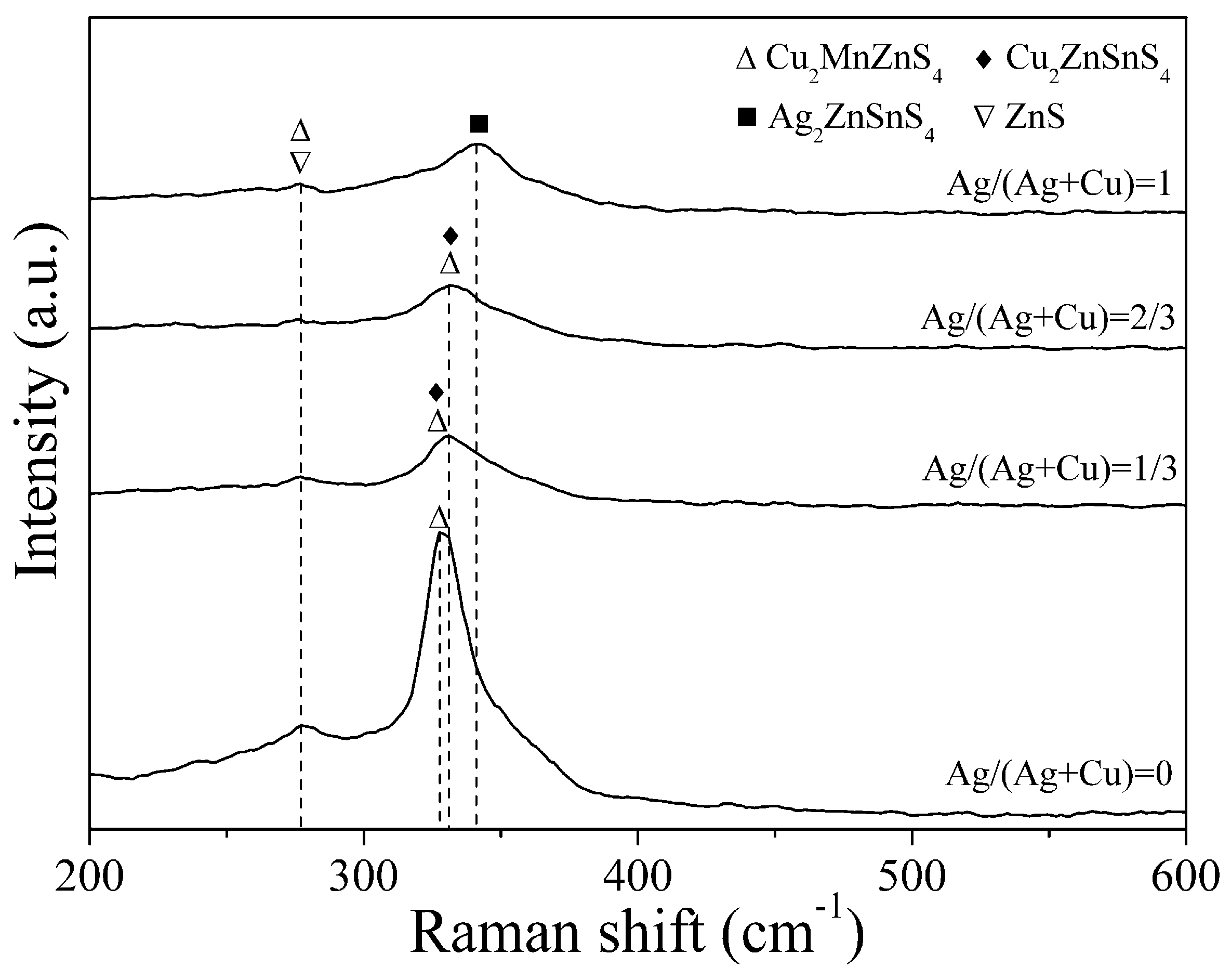
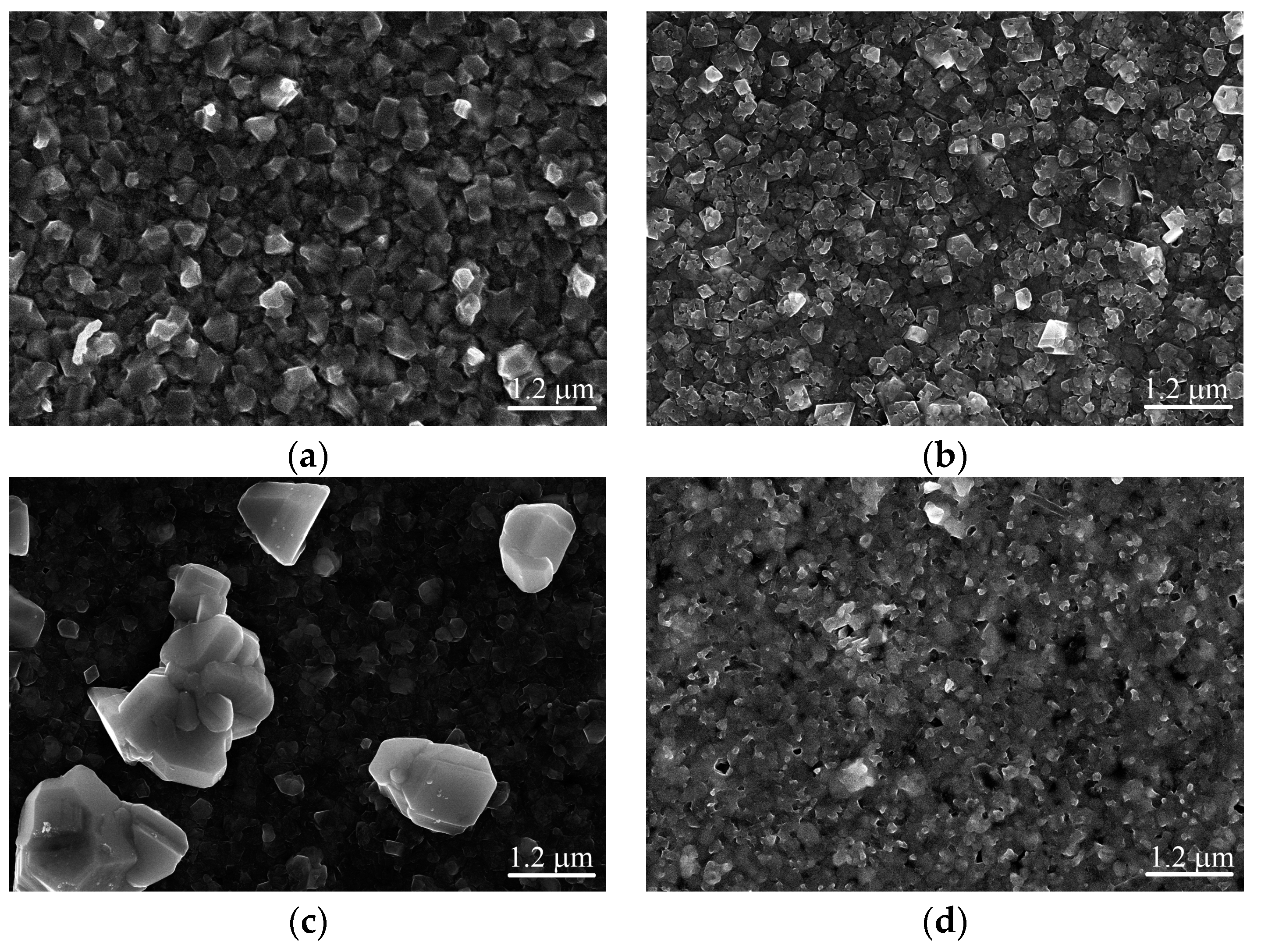
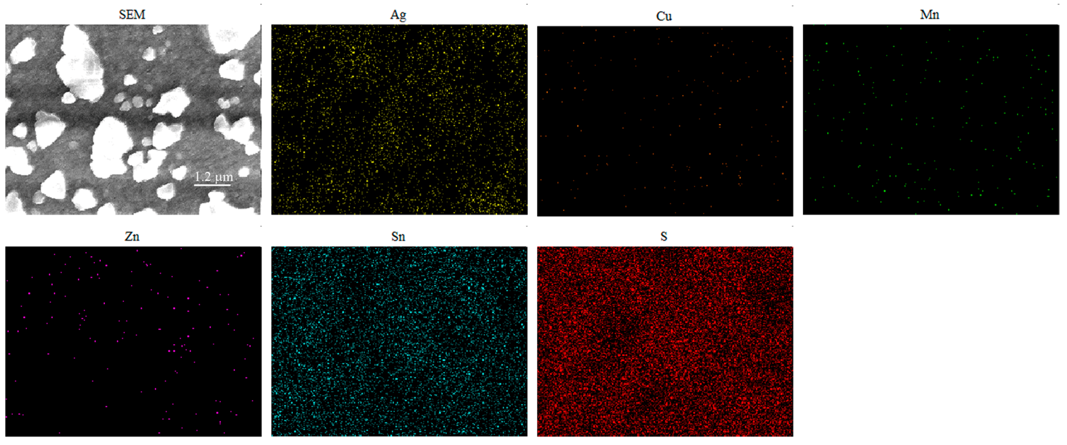
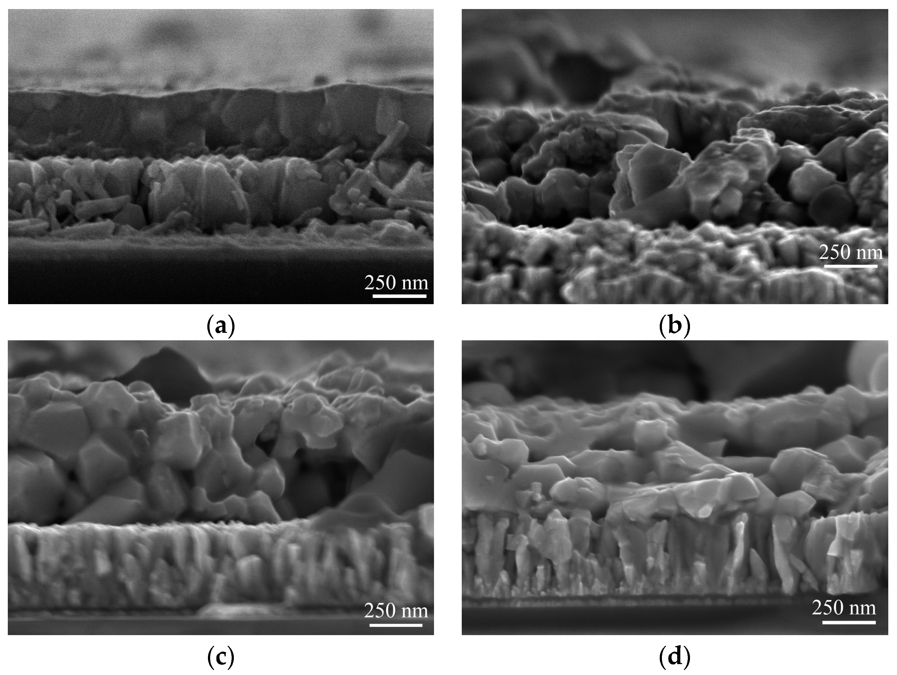
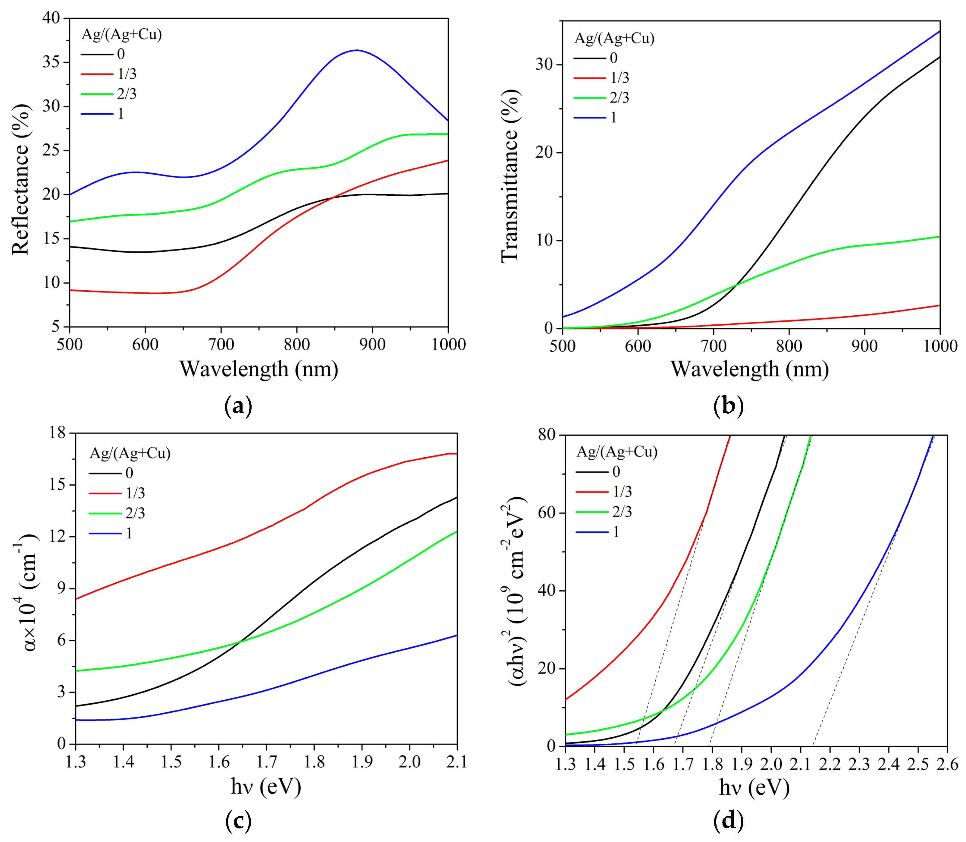
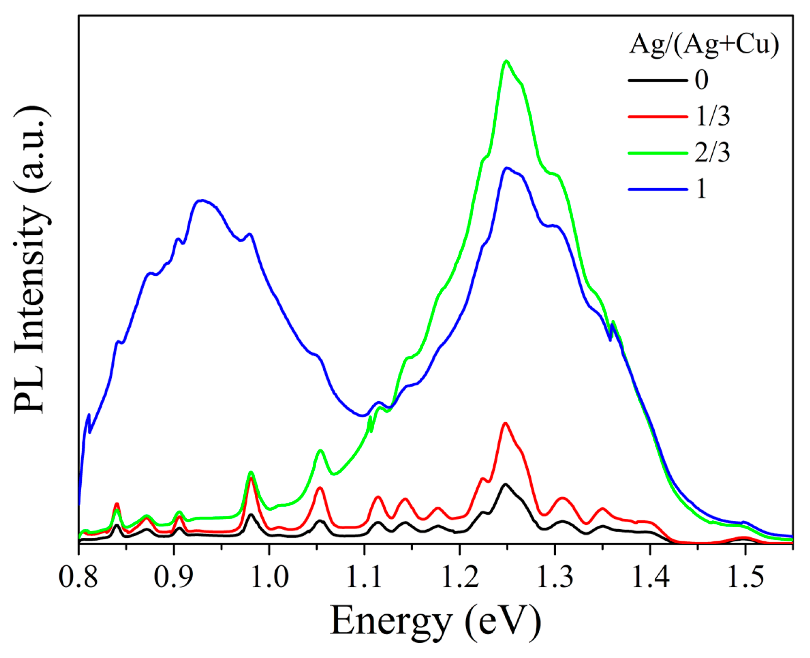
3. Results and Discussion

Figure 2 shows the XRD patterns of Ag and Mn co-doped Cu2ZnSnS4 thin films with different Ag amounts and the standard XRD peaks for Cu2ZnSnS4, Cu2MnSnS4, Ag2ZnSnS4, SnS2, and SnO2. The XRD pattern of Mn-doped Cu2ZnSnS4 thin film without Ag shows the strongest peak at 28.3°, which is between the positions of the peaks attributed to the (112) plane of Cu2MnSnS4 (28.2°) and the (112) plane of Cu2ZnSnS4 (28.5°). The diffraction peak at 47.2° in the pattern is attributed to the (220) plane of Cu2ZnSnS4. These results indicate the incorporation of Mn into Cu2ZnSnS4 lattice and the preferred orientation along the (112) plane. The peaks belonging to the secondary phase of SnS2 are detected at 14.7° and 49.4°. The SnO2 peaks originate from the FTO substrate. When Ag is introduced into Mn-doped Cu2ZnSnS4 with Ag/(Ag + Cu) = 1/3, the dominant diffraction peak is still located at 28.3° and becomes stronger. In addition, a weak peak appears at 27.8°, which is between the standard (112) peak of Ag2ZnSnS4 (27.3°) and the (112) peak of Cu2MnSnS4 (28.2°). Therefore, Ag and Mn co-doped Cu2ZnSnS4 structure is formed. When the atomic ratio of Ag/(Ag + Cu) increases to 2/3, the two peaks at around 28° slightly shift to the low diffraction angle direction due to the increase in the amount of Ag. The left side peak at 27.4° is stronger than that at 28.2° because the Ag amount is greater than the Mn amount in this sample. For the thin film with full substitution of Ag, the peak at 28.2° disappears. A main but weak peak located at 27.6° is related to Ag2ZnSnS4 or Cu2MnSnS4 phases. All the co-doped Cu2ZnSnS4 thin films have preferred orientation along the (112) plane. Secondary phase of SnS2 can be detected in all thin films.
Figure 3 shows the Raman spectra of Ag and Mn co-doped Cu2ZnSnS4 thin films with different Ag amounts. The strongest Raman characteristic peak of Mn single-doped Cu2ZnSnS4 thin film is located at 327 cm−1, matching with the reported position of the Cu2MnZnS4 peak [20,21]. The thin films with Ag/(Ag + Cu) = 1/3 and Ag/(Ag + Cu) = 2/3 show a Cu2ZnSnS4 or Cu2MnZnS4 peak at 331 cm−1 [20,22,23]. For the thin film with full Ag substitution, the Raman peak at 342 cm−1 is near the reported Ag2ZnSnS4 peak [24]. The weak peaks at 277 cm−1 in all thin films originate from the vibrational mode of Cu2MnZnS4 [23] or ZnS [25]. The strongest Raman peak shifts to a higher Raman shift direction with increasing Ag amount due to the change of phase structure from Cu2MnZnS4 to Ag2ZnSnS4. The SnS2 secondary phase detected by XRD has Raman shifts of 215 cm−1 and 315 cm−1 [26]. However, all the prepared thin films do not show the Raman peak of SnS2. Since Raman scattering measurement is surface-sensitive, the SnS2 phase may locate near the back of thin film and cannot be detected by Raman measurement. Ag or Mn secondary phase is absent in the Raman spectra. The measured results of XRD and Raman confirm the successful formation of Ag and Mn co-doped kesterite Cu2ZnSnS4 thin films without a secondary phase related to Ag or Mn.
Table 1 provides the atomic percentages of Ag, Cu, Mn, Zn, Sn, and S in the prepared samples. The calculated atomic ratios of Ag/(Ag + Cu), Mn/(Mn + Zn), (Cu + Ag)/(Mn + Zn), and S/(Ag + Cu) of each sample are also given in Table 1. During EDS measurement, only the Ag, Cu, Mn, Zn, Sn, and S elements in the thin film were considered and the Si, O, and other elements were ignored. It is noted that the atomic percentage of Sn in the thin film is lower than the measured value because the Sn element in FTO contributes to the measured result. The Ag/(Ag + Cu) ratios of Cu2ZnSnS4 thin films are close to those of sols, indicating the effective incorporation of Ag into Cu2ZnSnS4 thin films. However, the measured Mn/(Mn + Zn) ratios of thin films are lower than those of sols due to the precipitation of Mn during sol preparations. The value of S/(Ag + Cu) approaches the stoichiometry of 2 with increasing Ag amount.
Figure 4 shows the surface SEM images of Ag and Mn co-doped Cu2ZnSnS4 thin films with different Ag amounts. In Figure 4a, for the Mn-doped Cu2ZnSnS4 thin film without Ag doping, grains with size of about 300 nm distribute on the thin film surface. After Ag incorporation with Ag/(Ag + Cu) = 1/3, the thin film surface becomes more compact and the grain size is about 280 nm. When Ag/(Ag + Cu) = 2/3, the surface of thin film is crack-free and consists of isolated, discontinuous, and large grains with a maximum size of around 2 μm and small grains with size of about 300 nm. EDS mapping was further performed for this sample and the results are given in Figure 5. Although there is slight inhomogeneity of element distribution in the thin film, all the six elements distribute in both large and small grains. Therefore, both grains are Ag and Mn co-doped Cu2ZnSnS4. In Figure 4d, when Cu is fully substituted by Ag the grain size significantly reduces and the grains become fuzzy. Meanwhile, pinholes increase and enlarge in the thin film surface. As revealed from XRD results, the co-doped thin films contain a secondary phase of SnS2. Since SnS2 is volatile at high temperature, these pinholes may result from the evaporation of SnS2 during thin film fabrications. There is residual SnS2 in the final thin film.
The cross-section SEM images of Cu2ZnSnS4 samples in Figure 6 show Cu2ZnSnS4/FTO/glass stacked structure. The thin film with Mn single doping has homogeneous, smooth, and compact cross-section morphology, but the grain is hard to detect. After Ag co-doping, grainy morphologies can be seen in the cross-sections of thin films. The thickness of co-doped Cu2ZnSnS4 thin films is 650 nm. There are some pinholes in the co-doped thin films and at the Cu2ZnSnS4/FTO interfaces, which may result from the evaporation of SnS2 secondary phase as mentioned previously.
Figure 7 shows the reflectance (R), transmittance (T), absorption coefficient (α), and (αhυ)2 versus relations of prepared thin films, where is photon energy. The reflectance of all Cu2ZnSnS4 samples in the wavelength range of 500 to 1000 nm is lower than 37%. The average reflectances of Cu2ZnSnS4 thin films with Ag/(Ag + Cu) ratios of 0, 1/3, 2/3, and 1 are 16.7%, 15.0%, 21.5%, and 27.5%, respectively. The transmittance of samples decreases with the reduction of wavelength due to the absorption in Cu2ZnSnS4. The absorption coefficient of thin film is calculated by the following equation [27]:
α = 1 d ln ( T 2 ( 1 R ) 2 + 4 T 2 + ( ( 1 R ) 2 T 2 ) 2 2 T ) ,
where d is the thickness of thin film. As shown in Figure 7c, the absorption coefficients of Ag and Mn co-doped Cu2ZnSnS4 thin films are larger than 1.3 × 104 cm−1 for photon energy greater than 1.3 eV. Compared with Mn single-doped thin film, Ag co-doping with a suitable amount can increase the absorption coefficient of Cu2ZnSnS4 thin films. According to the relation of (αhυ)2 = C(Eg), where C is a constant and Eg is direct optical band gap, the Eg of Cu2ZnSnS4 thin film can be obtained from the (αhυ)2 curves in Figure 7d. The intercept on the axis of the extrapolation of the linear region of (αhυ)2 curve gives the Eg values of 1.67, 1.54, 1.78, and 2.14 eV for Cu2ZnSnS4 thin films with Ag/(Ag + Cu) ratios of 0, 1/3, 2/3, and 1, respectively. The Eg of co-doped Cu2ZnSnS4 thin film increases with the increasing Ag/(Ag + Cu) ratio due to Ag doping. It is reported that the band gap of Ag single-doped Cu2ZnSnS4 thin film becomes increasingly wide with the increase of Ag concentration [12,13].
Figure 8 shows photoluminescence spectra of single-doped and co-doped Cu2ZnSnS4 thin films. Compared with the Mn single-doped Cu2ZnSnS4 thin film, all the Ag and Mn co-doped Cu2ZnSnS4 thin films show enhanced photoluminescence, especially the thin films with Ag/(Ag + Cu) ratios of 2/3 and 1. This indicates that Ag and Mn co-doping can reduce the harmful defect states and nonradiative recombination in Cu2ZnSnS4 thin film by double cation substitutions.
Compared with the Mn single-doped Cu2ZnSnS4 thin films in this study and previously reported results [28,29,30], a further incorporation of Ag with suitable doping concentration can promote grain growth, increase the absorption coefficient of thin film, expand the adjustment range of the band gap of thin film, and reduce the nonradiative recombination in the thin film.

4. Conclusions

Ag and Mn co-doped Cu2ZnSnS4 thin films with different Ag amounts were successfully fabricated on FTO-coated glass substrates by sol–gel and spin-coating techniques. The XRD and Raman measurements reveal the formation of Ag and Mn co-doped Cu2ZnSnS4 with preferred orientation of the (112) plane and without Ag or Mn secondary phase. The atomic ratios of Ag/(Ag + Cu) in the Cu2ZnSnS4 thin films are close to those of original sols. Ag co-doping can enhance the grain size and absorption coefficient of Cu2ZnSnS4 thin films. The thickness and direct optical band gap of Ag and Mn co-doped Cu2ZnSnS4 thin films are 650 nm and 1.54–2.14 eV, respectively. The Ag and Mn co-doped Cu2ZnSnS4 thin films show an enhanced photoluminescence property, indicating the beneficial effects of reduced defects and nonradiative recombination by Ag and Mn co-doping. This work reveals potential advantages of Ag and Mn co-doping on Cu2ZnSnS4 thin film.

Author Contributions

Conceptualization, L.Q. and J.X.; Data curation, L.Q. and X.T.; Funding acquisition, J.X.; Investigation, L.Q. and X.T.; Supervision, J.X.; Validation, X.T.; Writing—Original draft, L.Q. and J.X.; Writing—Review & editing, J.X.

Funding

This research was funded by National Natural Science Foundation of China, grant number 61504029 and Science and Technology Planning Project of Guangdong Province, China, grant number 2017A010104017.

Conflicts of Interest

The authors declare no conflict of interest. The funders had no role in the design of the study; in the collection, analyses, or interpretation of data; in the writing of the manuscript, or in the decision to publish the results.

References

  1. Wibowo, R.A. Powder-to-film approach for fabricating critical raw material-free kesterite Cu2ZnSn(S,Se)4 thin film photovoltaic: A review. Sol. Energy 2018, 176, 157–169. [Google Scholar] [CrossRef]
  2. Shi, Z.Q.; Attygalle, D.; Jayatissa, A.H. Kesterite-based next generation high performance thin film solar cell: Current progress and future prospects. J. Mater. Sci. Mater. Electron. 2017, 28, 2290–2306. [Google Scholar] [CrossRef]
  3. Zhang, C.J.; Tao, J.H.; Chu, J.H. An 8.7% efficiency co-electrodeposited Cu2ZnSnS4 photovoltaic device fabricated via a pressurized post-sulfurization process. J. Mater. Chem. C 2018, 6, 13275–13282. [Google Scholar] [CrossRef]
  4. Jiang, J.C.; Zhang, L.Q.; Wang, W.; Hong, R.J. The role of sulphur in the sulfurization of CZTS layer prepared by DC magnetron sputtering from a single quaternary ceramic target. Ceram. Int. 2018, 44, 11597–11602. [Google Scholar] [CrossRef]
  5. Yan, C.; Huang, J.L.; Sun, K.W.; Johnston, S.; Zhang, Y.F.; Sun, H.; Pu, A.B.; He, M.R.; Liu, F.Y.; Eder, K. Cu2ZnSnS4 solar cells with over 10% power conversion efficiency enabled by heterojunction heat treatment. Nat. Energy 2018, 3, 764–772. [Google Scholar] [CrossRef]
  6. Wang, W.; Winkler, M.T.; Gunawan, O.; Gokmen, T.; Todorov, T.K.; Zhu, Y.; Mitzi, D.B. Device characteristics of CZTSSe thin-film solar cells with 12.6% efficiency. Adv. Energy Mater. 2014, 4, 1301465. [Google Scholar] [CrossRef]
  7. Pal, K.; Singh, P.; Bhaduri, A.; Thapa, K.B. Current challenges and future prospects for a highly efficient (>20%) kesterite CZTS solar cell: A review. Sol. Energy Mater. Sol. Cells. 2019, 196, 138–156. [Google Scholar] [CrossRef]
  8. Li, W.; Liu, X.L.; Cui, H.T.; Huang, S.J.; Hao, X.J. The role of Ag in (Ag, Cu)2ZnSnS4 thin film for solar cell application. J. Alloys Compd. 2015, 625, 277–283. [Google Scholar] [CrossRef]
  9. Zhao, Y.; Han, X.X.; Xu, B.; Li, W.; Li, J.; Li, J.J.; Wang, M.; Dong, C.; Ju, P.; Li, J.S. Enhancing open-circuit voltage of solution-processed Cu2ZnSn(S,Se)4 solar cells with Ag substitution. IEEE J. Photovolt. 2017, 7, 874–881. [Google Scholar] [CrossRef]
  10. Henry, J.; Mohanraj, K.; Sivakumar, G. Vacuum evaporated FTO/(Cu, Ag)2ZnSnSe4 thin films and its electrochemical analysis. Vacuum 2019, 160, 347–354. [Google Scholar] [CrossRef]
  11. Nguyen, T.H.; Kawaguchi, T.; Chantana, J.; Minemoto, T.; Harada, T.; Nakanishi, S.; Ikeda, S. Structural and solar cell properties of a Ag-containing Cu2ZnSnS4 thin film derived from spray pyrolysis. ACS Appl. Mater. Interfaces 2018, 10, 5455–5463. [Google Scholar] [CrossRef]
  12. Kumar, J.; Ingole, S. Structural and optical properties of (AgxCu1-x)2ZnSnS4 thin films synthesised via solution route. J. Alloys Compd. 2017, 727, 1089–1094. [Google Scholar] [CrossRef]
  13. Chen, X.Y.; Wang, J.L.; Zhou, W.H.; Chang, Z.X.; Kou, D.X.; Zhou, Z.J.; Tian, Q.W.; Meng, Y.N.; Wu, S.X. Rational synthesis of (Cu1-xAgx)2ZnSnS4 nanocrystals with low defect and tuning band gap. Mater. Lett. 2016, 181, 317–320. [Google Scholar] [CrossRef]
  14. Kumar, M.S.; Madhusudanan, S.P.; Batabyal, S.K. Substitution of Zn in earth-abundant Cu2ZnSn(S,Se)4 based thin film solar cells—A status review. Sol. Energy Mater. Sol. Cells. 2018, 185, 287–299. [Google Scholar] [CrossRef]
  15. Su, Z.H.; Tan, J.M.R.; Li, X.L.; Zeng, X.; Batabyal, S.K.; Wong, L.H. Cation substitution of solution-processed Cu2ZnSnS4 thin film solar cell with over 9% efficiency. Adv. Energy Mater. 2015, 5, 1500682. [Google Scholar] [CrossRef]
  16. Yan, C.; Sun, K.W.; Huang, J.L.; Johnston, S.; Liu, F.Y.; Puthen, B.; Veettil, B.P.; Sun, K.L.; Pu, A.B.; Zhou, F.Z.; et al. Beyond 11% efficient sulfide Kesterite Cu2ZnxCd1-xSnS4 solar cell: Effects of cadmium alloying. ACS Energy Lett. 2017, 2, 930–936. [Google Scholar] [CrossRef]
  17. Ananthoju, B.; Mohapatra, J.; Jangid, M.K.; Bahadur, D.; Medhekar, N.V.; Aslam, M. Cation/anion substitution in Cu2ZnSnS4 for improved photovoltaic performance. Sci. Rep. 2016, 6, 35369. [Google Scholar] [CrossRef]
  18. Huang, K.L.; Huang, C.H.; Lin, W.T.; Fu, Y.S.; Guo, T.F. Solvothermal synthesis and tunable bandgap of Cu2(Zn1-xCox)SnS4 and Cu2(Fe1-xCox)SnS4 nanocrystals. J. Alloys Compd. 2015, 646, 1015–1022. [Google Scholar] [CrossRef]
  19. Hadke, S.H.; Levcenko, S.; Lie, S.; Hages, C.J.; Marquez, J.A.; Unold, T.; Wong, L.H. Synergistic effects of double cation substitution in solution-processed CZTS solar cells with over 10% efficiency. Adv. Energy Mater. 2018, 8, 1802540. [Google Scholar] [CrossRef]
  20. Wang, W.H.; Chen, B.W.; Chen, G.L.; Cai, H.L.; Dong, J.B.; Liao, Y.B.; Chen, S.Y.; Huang, Z.G. A general oxide-based preparation strategy for Cu2MSnS4 (M: Zn, Mn, Cd) thin films and relevant solar cells. Mater. Lett. 2018, 214, 170–173. [Google Scholar] [CrossRef]
  21. Yu, J.J.; Deng, H.M.; Tao, J.H.; Chen, L.L.; Cao, H.Y.; Sun, L.; Yang, P.X.; Chu, J.H. Synthesis of Cu2MnSnS4 thin film deposited on seeded fluorine doped tin oxide substrate via a green and low-cost electrodeposition method. Mater. Lett. 2017, 191, 186–188. [Google Scholar] [CrossRef]
  22. Jiang, Y.H.; Yao, B.; Li, Y.F.; Ding, Z.H.; Luan, H.M.; Jia, J.H.; Li, Y.; Shi, K.; Sui, Y.R.; Zhang, B.Y. Structure, optical and electrical properties of (Cu1-xAgx)2ZnSn(S,Se)4 alloy thin films for photovoltaic application. Mater. Sci. Semicond. Process. 2018, 81, 54–59. [Google Scholar] [CrossRef]
  23. Le Donne, A.; Marchionna, S.; Acciarri, M.; Cernuschi, F.; Binetti, S. Relevant efficiency enhancement of emerging Cu2MnSnS4 thin film solar cells by low temperature annealing. Sol. Energy 2017, 149, 125–131. [Google Scholar] [CrossRef]
  24. Ma, C.H.; Guo, H.F.; Zhang, K.Z.; Yuan, N.Y.; Ding, J.N. Fabrication of p-type kesterite Ag2ZnSnS4 thin films with a high hole mobility. Mater. Lett. 2017, 186, 390–393. [Google Scholar] [CrossRef]
  25. Serrano, J.; Cantarero, A.; Cardona, M.; Garro, N.; Lauck, R.; Tallman, R.E.; Ritter, T.M.; Weinstein, B.A. Raman scattering in β-ZnS. Phys. Rev. B 2004, 69, 014301. [Google Scholar] [CrossRef]
  26. Price, L.S.; Parkin, I.P.; Hardy, A.M.E.; Clark, R.J.H.; Hibbert, T.G.; Molloy, K.C. Atmospheric pressure chemical vapor deposition of tin sulfides (SnS,Sn2S3, and SnS2) on glass. Chem. Mater. 1999, 11, 1792–1799. [Google Scholar] [CrossRef]
  27. Kuzyutkina, Y.S.; Romanova, E.A.; Kochubei, V.I.; Shiryaev, V.S. Specific features of linear and nonlinear optical responses of chalcogenide glasses in the As-S-Se and As-Se-Te systems. Opt. Spectrosc. 2014, 117, 53–59. [Google Scholar] [CrossRef]
  28. Lie, S.; Sandi, M.I.; Tay, Y.F.; Li, W.J.; Tan, J.M.R.; Bishop, D.M.; Gunawan, O.; Wong, L.H. Improving the charge separation and collection at the buffer/absorber interface by double-layered Mn-substituted CZTS. Sol. Energy Mater. Sol. Cells. 2018, 185, 351–358. [Google Scholar] [CrossRef]
  29. Chen, L.L.; Deng, H.M.; Cui, J.Y.; Tao, J.H.; Zhou, W.L.; Cao, H.Y.; Sun, L.; Yang, P.X.; Chu, J.H. Composition dependence of the structure and optical properties of Cu2MnxZn1-xSnS4 thin films. J. Alloys Compd. 2015, 627, 388–392. [Google Scholar] [CrossRef]
  30. Guan, H.; Shen, H.; Li, J. Synthesis and optical properties of Cu2(Zn1-XMnX)SnS4 thin films with tunable band gap. Chalcogenide Lett. 2017, 14, 217–221. [Google Scholar]
Figure 1. Flow chart for the fabrication process of Ag and Mn co-doped Cu2ZnSnS4 thin films.
Nanomaterials 09 01520 g001
Figure 2. XRD patterns of Ag and Mn co-doped Cu2ZnSnS4 thin films with different Ag/(Ag + Cu) ratios and the standard XRD peaks for Cu2ZnSnS4, Cu2MnSnS4, Ag2ZnSnS4, SnS2, and SnO2.
Nanomaterials 09 01520 g002
Figure 3. Raman spectra of Ag and Mn co-doped Cu2ZnSnS4 thin films with different Ag/(Ag + Cu) ratios.
Nanomaterials 09 01520 g003
Figure 4. Surface SEM images of Ag and Mn co-doped Cu2ZnSnS4 thin films with (a) Ag/(Ag + Cu) = 0; (b) Ag/(Ag + Cu) = 1/3; (c) Ag/(Ag + Cu) = 2/3; and (d) Ag/(Ag + Cu) = 1.
Nanomaterials 09 01520 g004
Figure 5. EDS mapping results for Ag and Mn co-doped Cu2ZnSnS4 thin film with Ag/(Ag + Cu) = 2/3.
Nanomaterials 09 01520 g005
Figure 6. Cross-section SEM images of Ag and Mn co-doped Cu2ZnSnS4 samples with (a) Ag/(Ag + Cu) = 0; (b) Ag/(Ag + Cu) = 1/3; (c) Ag/(Ag + Cu) = 2/3; and (d) Ag/(Ag + Cu) = 1.
Nanomaterials 09 01520 g006
Figure 7. The (a) reflectance; (b) transmittance; (c) absorption coefficient; and (d) (αhυ)2 versus relations of Ag and Mn co-doped Cu2ZnSnS4 thin films with different Ag/(Ag + Cu) ratios.
Nanomaterials 09 01520 g007
Figure 8. Photoluminescence spectra of Mn single-doped and Ag and Mn co-doped Cu2ZnSnS4 thin films with different Ag/(Ag + Cu) ratios.
Nanomaterials 09 01520 g008
Table 1. The compositions of Ag and Mn co-doped Cu2ZnSnS4 thin films.
CompositionAg/(Ag + Cu) in Sol
01/32/31
Ag (at.%)05.88 ± 0.0311.93 ± 0.4421.09 ± 0.82
Cu (at.%)17.46 ± 0.139.37 ± 0.156.07 ± 0.440.33 ± 0.03
Mn (at.%)2.29 ± 0.152.55 ± 0.072.37 ± 0.102.04 ± 0.16
Zn (at.%)7.06 ± 0.216.07 ± 0.455.58 ± 0.615.71 ± 0.30
Sn (at.%)25.89 ± 0.3029.65 ± 0.6826.29 ± 0.8721.90 ± 0.41
S (at.%)47.31 ± 0.5246.50 ± 0.4447.76 ± 1.0448.93 ± 1.44
Ag/(Ag + Cu)00.390.660.98
Mn/(Mn + Zn)0.240.300.300.26
(Cu + Ag)/(Mn + Zn)1.871.772.262.76
S/(Ag + Cu)2.713.052.652.28

