Article

Ultra-High Refractive Index Sensing Structure Based on a Metal-Insulator-Metal Waveguide-Coupled T-Shape Cavity with Metal Nanorod Defects

by
Yuan-Fong Chou Chau
1,*,
Chung-Ting Chou Chao
2,
Hung Ji Huang
3,
N. T. R. N. Kumara
1,
Chee Ming Lim
1 and
Hai-Pang Chiang
2,4,*
1
Centre for Advanced Material and Energy Sciences, Universiti Brunei Darussalam, Tungku Link, Gadong BE1410, Negara Brunei Darussalam
2
Institute of Optoelectronic Sciences, National Taiwan Ocean University, No. 2 Pei-Ning Rd., Keelung 202, Taiwan
3
Taiwan Instrument Research Institute, National Applied Research Laboratories, Hsinchu 300, Taiwan
4
Institute of Physics, Academia Sinica, Taipei 115, Taiwan
*
Authors to whom correspondence should be addressed.
Nanomaterials 2019, 9(10), 1433; https://doi.org/10.3390/nano9101433
Submission received: 10 September 2019 / Revised: 1 October 2019 / Accepted: 8 October 2019 / Published: 10 October 2019
(This article belongs to the Special Issue Nanobiophotonics, Photomedicine, and Imaging)

Abstract

:
An ultra-high plasmonic refractive index sensing structure composed of a metal–insulator–metal (MIM) waveguide coupled to a T-shape cavity and several metal nanorod defects is proposed and investigated by using finite element method. The designed plasmonic MIM waveguide can constitute a cavity resonance zone and the metal nanorod defects can effectively trap the light in the T-shape cavity. The results reveal that both the size of defects in wider rectangular cavity and the length of narrower rectangular cavity are primary factors increasing the sensitivity performance. The sensitivity can achieve as high as 8280 nm/RIU (RIU denotes the refractive index unit), which is the highest sensitivity reported in plasmonic MIM waveguide-based sensors to our knowledge. In addition, the proposed structure can also serve as a temperature sensor with temperature sensitivity as high as 3.30 nm/°C. The designed structure with simplicity and ease of fabrication can be applied in sensitivity nanometer scale refractive index sensor and may potentially be used in optical on-chip nanosensor.

Graphical Abstract

1. Introduction

Surface plasmon polaritons (SPPs) are electromagnetic (EM) waves coherently coupled to electron oscillations which travel at the boundary between a metal and a dielectric [1,2,3], with evanescently decaying EM waves in both borders, which propagate along the metal–dielectric interface [4]. SPP waveguide structures [5,6,7], in particular, metal–insulator–metal (MIM) waveguides [8] with small size, ease of integration, and good balance between light localization and propagation loss [9], have attracted much attention with expectations to realize highly integrated optical circuits because of their behaviour of overcoming the diffraction limit of light [10]. Recently, several plasmonic MIM waveguide sensors have been proposed [11,12] and have been used to the development of sub-wavelength photonic devices such as splitters [13], couplers [14], and filters [15,16,17,18,19,20]. These devices basically consist of waveguides and resonators (or cavities). Because the MIM waveguide sensor is easy to connect with the sensing medium compared to the other sensor structures (e.g., photonic crystal fiber (PCF) sensor [21]) for detecting and sensing applications, many plasmonic MIM waveguide sensor structures have been explored based on surface plasmon resonance (SPR) [22,23] and cavity plasmon resonance (CPR) effects [7,24].
Mid-infrared (MIR) spectrum is in the wavelength range of 2 μm to 20 μm, which represents the molecular fingerprint zone [25], and the potential MIR applications have been widely reported in many works [26,27,28,29,30,31]. In particular, one of the purposes of plasmonic MIM waveguide sensors is necessary for atmospheric transparent window of MIR spectrum from 2 μm to 12 μm [32]. Although there have been reported a number of articles regarding diverse plasmonic MIM waveguides, the interaction nature of incident MIR EM wave and tunable MIM waveguide are investigated less. The necessity of tunable plasmonic MIM waveguide to achieve multifunctionalities in the MIR wavelength range grows into a possible approach for potential applications in chip-scale and integrated plasmonic devices. Plasmonic MIM waveguides necessitate being designed as simple and tuneable in a broadband spectrum if they are to be successfully implemented in sensing applications. The drawback of PCF sensors is that they are not suitable for chip-scale and integrated plasmonic devices. Compared with the PCF sensor [33], the sensitivity of MIM waveguides is much less than that of PCF sensor and still needs to be increased. Therefore, how to improve the sensitivity performance is a key issue in designing plasmonic MIM waveguide sensor.
In this paper, an ultra-high sensitivity of plasmonic structure based on MIM waveguide with a T-shape cavity and several silver nanorod defects compared with the case without the silver nanorod defects has been proposed and investigated. The transmittance spectrum properties of the proposed structure are investigated by means of finite element method (FEM) with perfect matched layers absorbing boundary condition. The sensitivity is calculated to characterize its sensing performance and filter properties. In the proposed MIM waveguide structure, a T-shape cavity is used and several silver nanorod defects are positioned in the T-shape cavity, such that it is approachable to the testing medium and ambient temperature. The T-shape cavity can constitute a resonance source and the silver nanorod defects can clasp the mode size in nanometer scale. The positions of transmission dips show a linear relationship with both RI of the material under RI sensing and surrounding temperature. Sensitivity obtained from the proposed structure reaches 8280 nm/RIU (where RIU is refractive index unit) and 3.30 nm/°C, respectively, which is far greater than the conventional RI sensors and temperature sensors [4,8,15,22,24]. This makes the designed MIM waveguide a promising plasmonic sensor that can provide a route for application in high-density photonic circuits and biosensors.

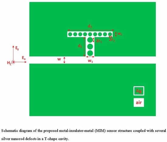
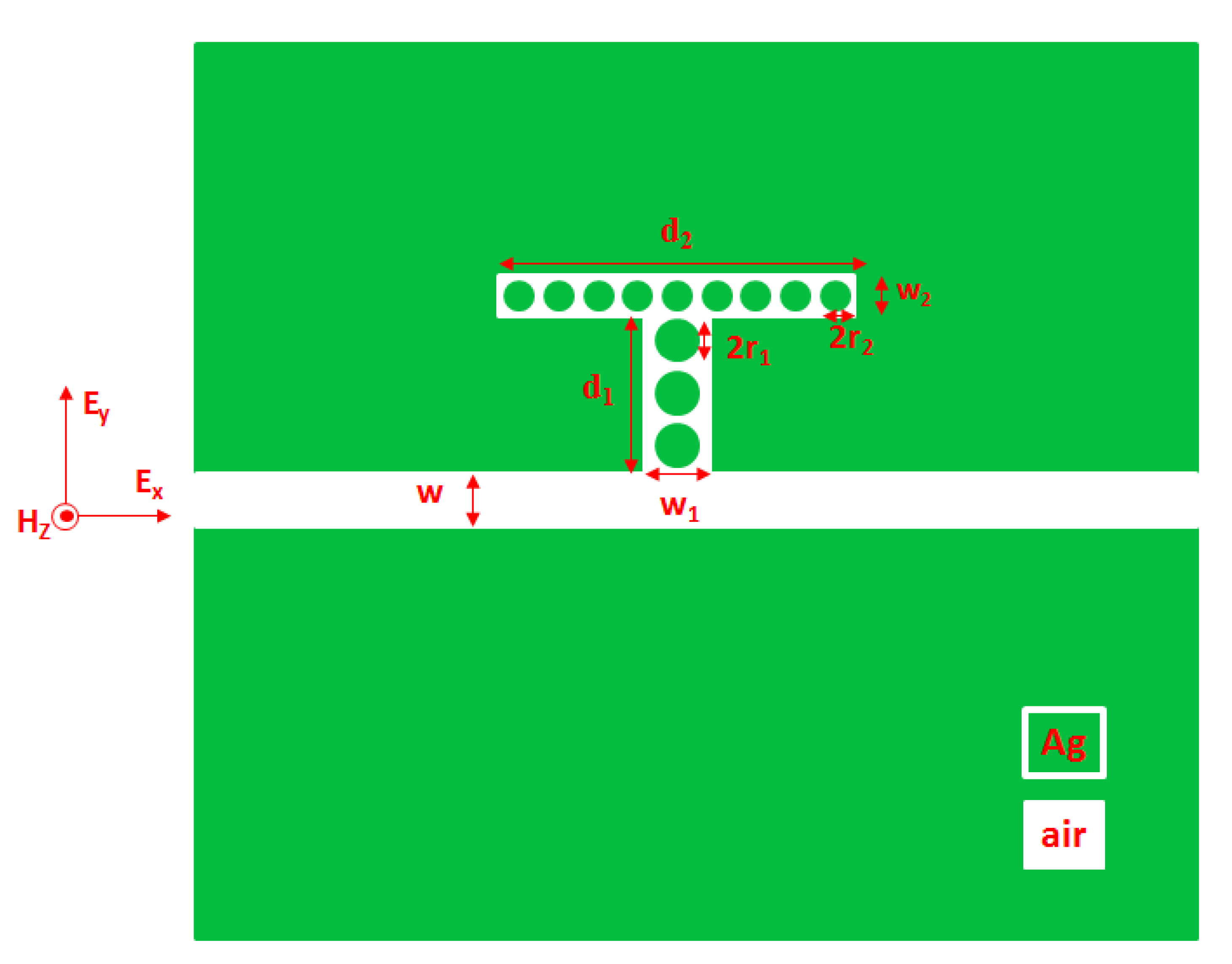
2. Simulation Method and Models

Figure 1 displays the schematic of a two-dimensional (2-D) plasmonic MIM waveguide structure which consists of a slit (with width w), a laterally coupled T-shape cavity and several silver nanorod defects in a T-shape cavity. The T-shape cavity is comprised of a wider rectangular cavity (with width w1 and length d1) and a narrower rectangular cavity (with width w2 and length d2). Three silver nanorods in wider rectangular cavity (radius r1) and nine silver nanorods in narrower rectangular cavity (radius r2) are uniformly distributed in the T-shape cavity. The distance between the center to the center of the adjacent silver nanorod is fixed to be 50 nm. The materials in white and green colors are set to be air and silver as shown in Figure 1. The testing liquid or gas is loaded in the waveguide slit and the T-shape cavity. In the practical situation, the liquid filling can be realized by capillary attraction. The incident EM wave can be coupled into the input port of waveguide by using nano-fiber (e.g., photonic crystal fiber (PCF) [34,35,36]) and the light in the output port of waveguide can be monitored by using Confocal Raman Microscopy [37].
The numerical simulation of the designed MIM waveguide was performed by using 2-D FEM (COMSOL multiphysics [38]) with perfect matched layer absorbing boundary conditions at all boundaries of the simulation region. The TM-polarized incident EM wave with inplane electric field components along the x-direction is directly coupled to the fundamental SPP mode [39]. Only the TM mode comprising of Ex, Ey and Hz components is considered because of its manifest plasmon phenomenon on the nanometal surface. The transmittance spectrum of the proposed plasmonic MIM waveguide are calculated by parameter scanning the incident wavelength in steps of 1 nm and the transmittance (T) is calculated by T = Pout/Pin, where the output power Pout and input power Pin are defined as integral values of energy flux density, respectively. The stable standing EM wave in the plasmonic MIM waveguide can only make up constructively within the T-shape cavity when the following resonant condition is satisfied [40]:
Δ φ = 2 π n ,
where n is the mode number which is a positive number (n = 1, 2, …).
If the resonance condition in the T-shape cavity is satisfied, the SPPs aroused in the slit would be coupled into the resonant T-shape cavity located next to the slit and develop a standing wave. The resonance wavelength (λres) is given by [7,41]:
λ r e s = 2   L n eff n φ ref π ,
where L is the effective length of the cavity (or resonator) and neff represents the real part of effective refractive index (RI) of the SPP, and φref is the phase shift of SPP reflection at the cavity metal wall. It can be observed that this has a linear relationship with the cavity length.
The frequency-dependent complex relative permittivity of silver is taken from [42]. The sensitivity (S) can be calculated as S = Δλ/Δn nanometer per refractive index (nm/RIU) [12,24,25,37,40], where Δλ is the shift of resonant peak wavelength of transmittance, λres is the resonant wavelength and Δn is the RI difference. The width of the slit waveguide (w) is kept constant to guarantee that only the fundamental transverse magnetic (TM0) mode is excited in the MIM waveguides [43]. The dispersion relation of the fundamental mode (TM0) in the proposed plasmonic MIM waveguide can be determined by the equation [44,45,46]:
ε d k 2 + ε m k 1 tan h ( k 1 2 ω ) = 0   ,
where km and kd are defined as: k 1 = β 2 ε d k 0 2 and k 2 = β 2 ε m k 0 2 ; here εm and εd are dielectric constants of the metal and dielectric, respectively. β stands for the constant of propagation for SPPs and k 0 = 2 π / λ 0 is the wave vector of light with wavelength λ 0 in free-space. The effective RI of the waveguide is denoted as neff = β/k0.

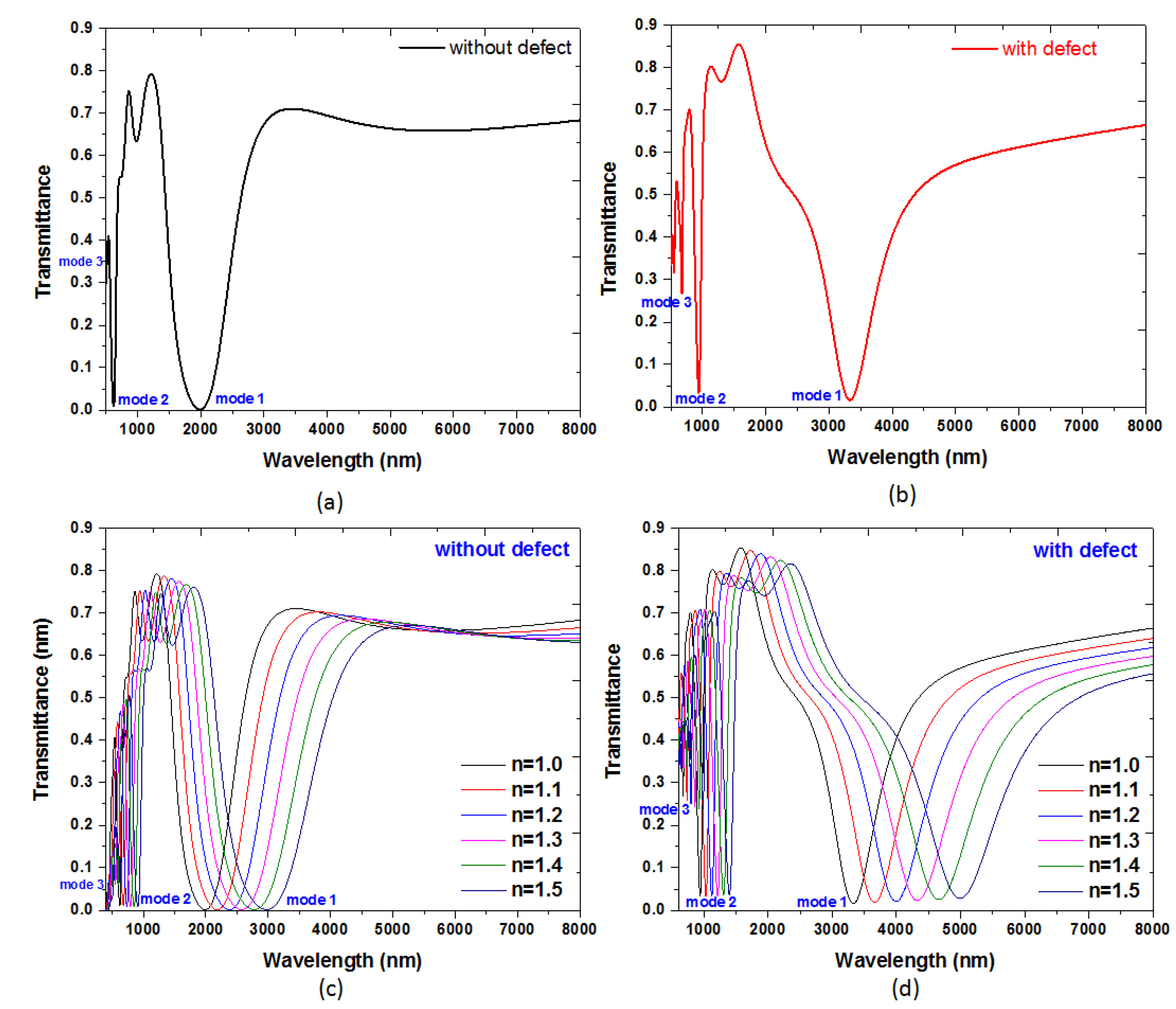
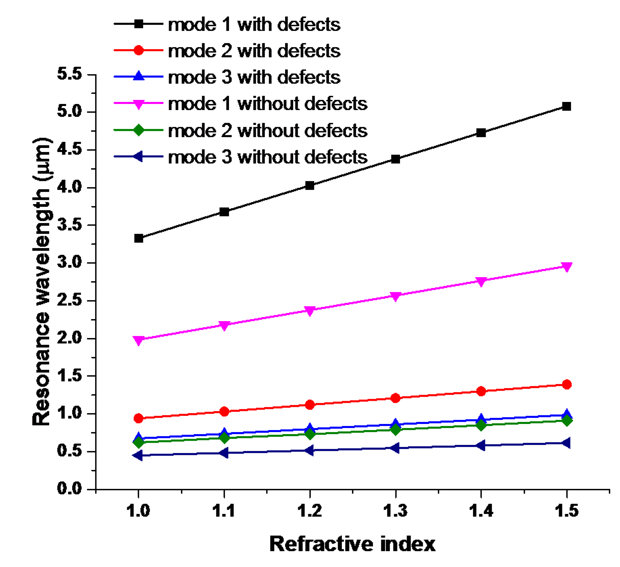
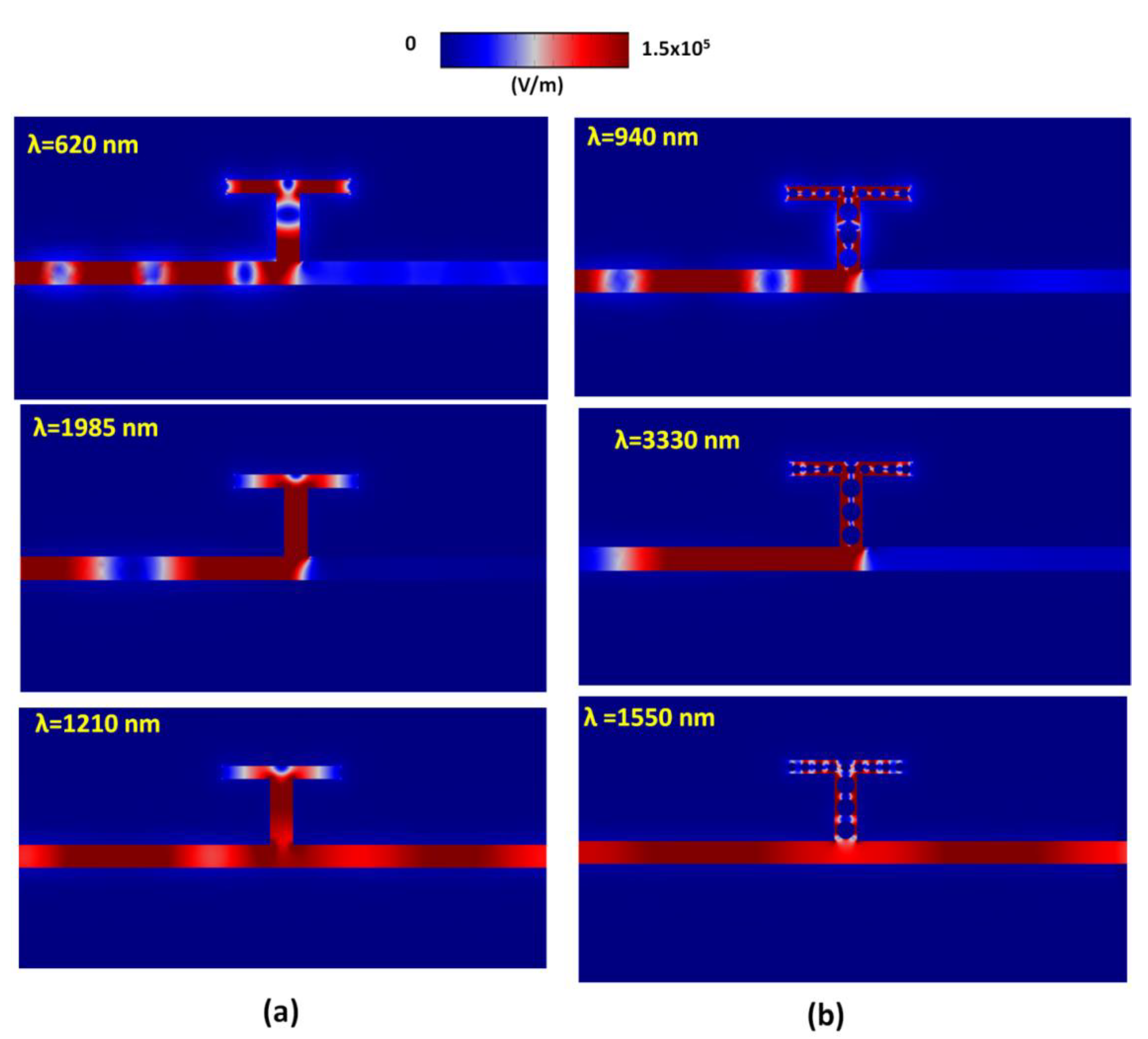
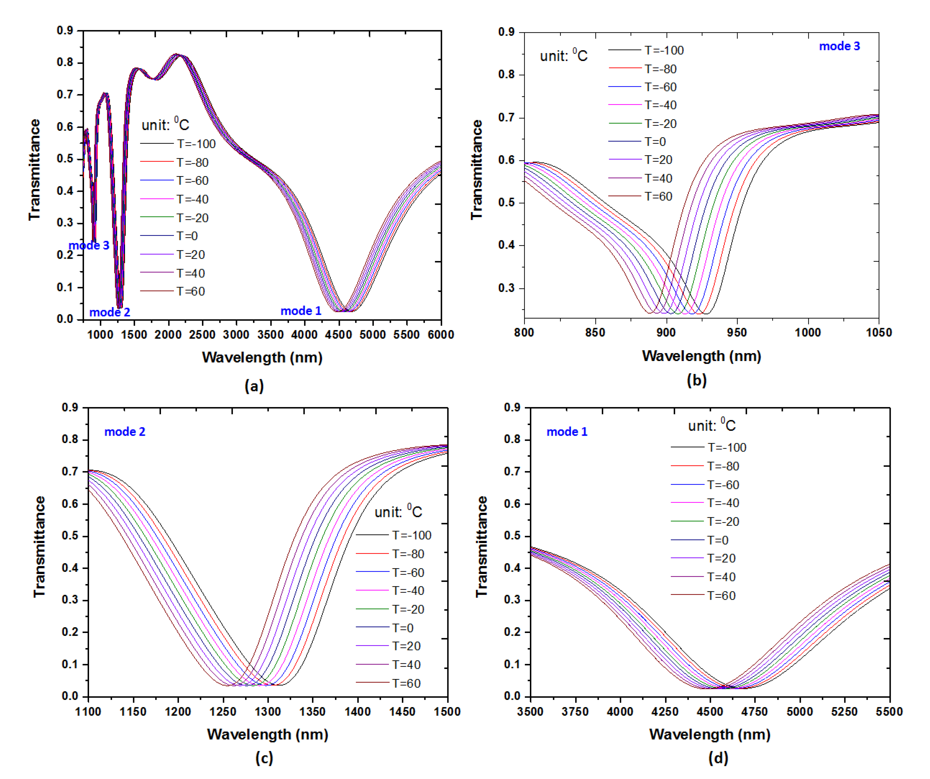
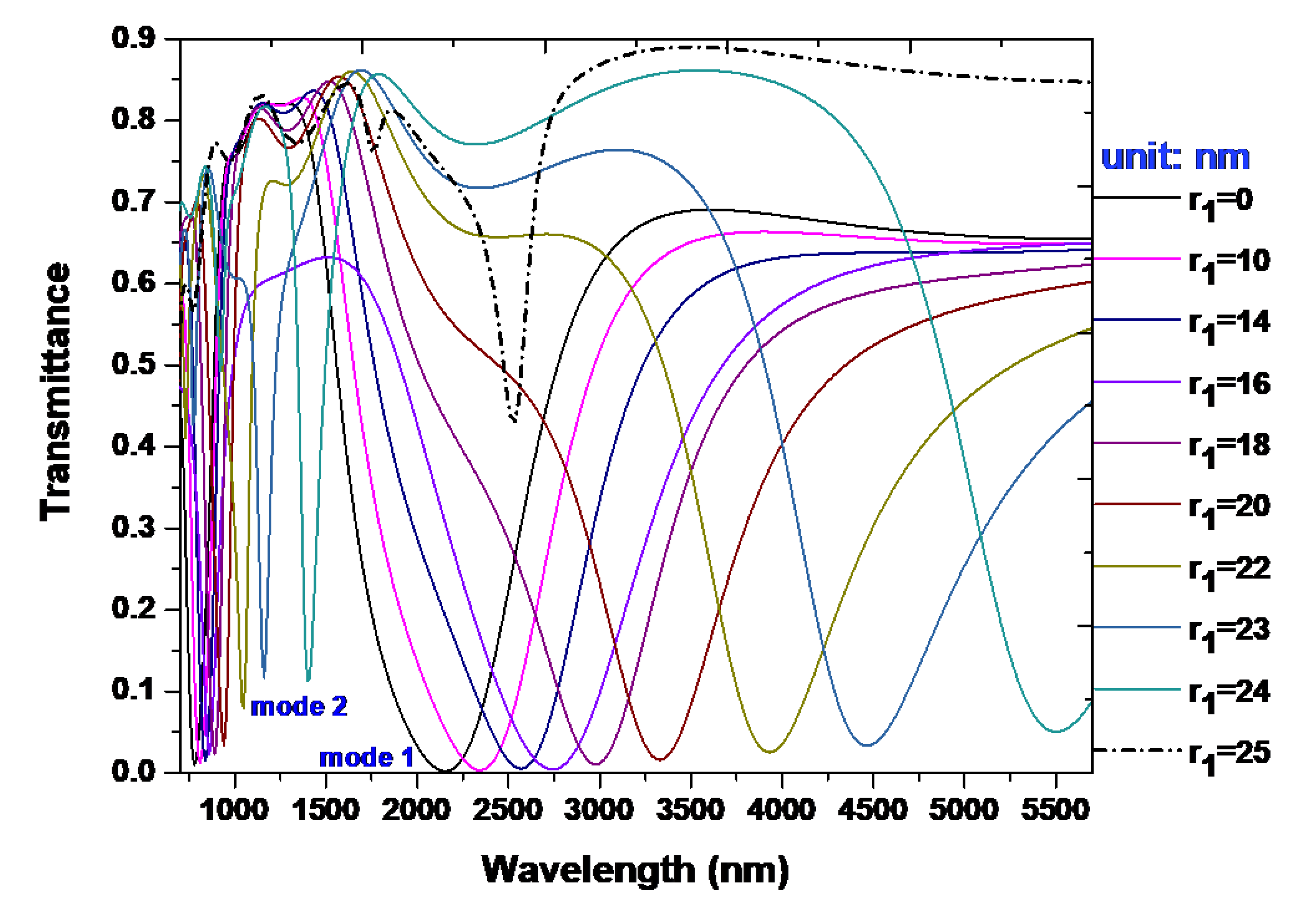
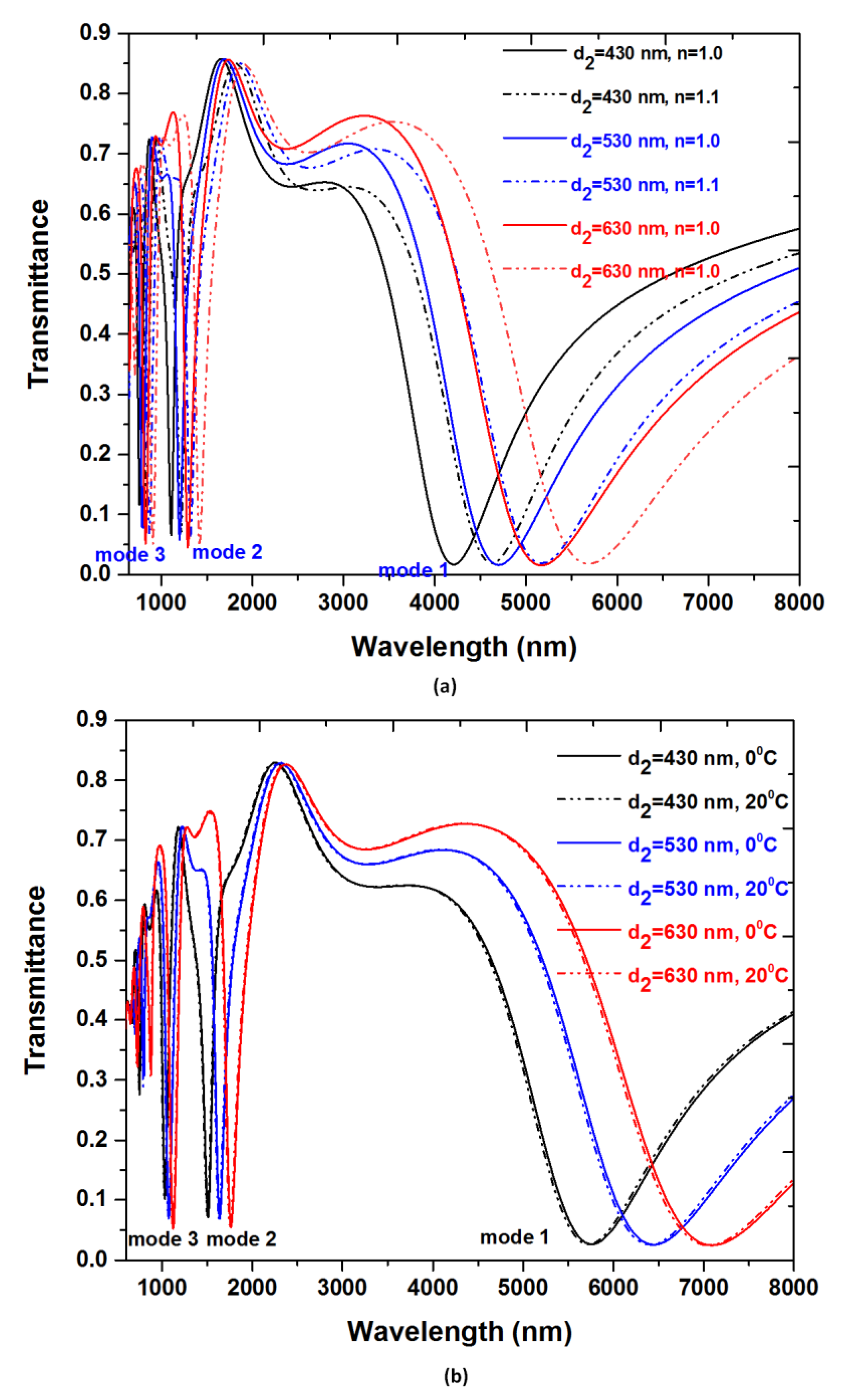
3. Results and Discussion

When the structural parameters of the proposed MIM waveguide, w, w1, w2, d1, d2, r1, r2, are set to be 50 nm, 50 nm, 30 nm, 150 nm, 330 nm, 20 nm and 10 nm, respectively, the transmittance spectra of the proposed plasmonic MIM waveguide without defects and without defects in the T-shape cavity are shown in Figure 2a,b, respectively. In Figure 2a,b, it is found that there are three distinct resonance dips occurred at λres = 1985 nm, 620 nm and 449 nm (i.e., mode 1, mode 2 and mode 3) for the case without defects and at λres = 3330 nm, 940 nm and 674 nm (i.e., mode 1, mode 2 and mode 3) for the case with detects, respectively. The distinct mode found in the case with defects is arisen from the silver nanorods in the T-shape cavity. When the incident EM wave propagates along the slit of the waveguide, the EM energy can couple to the T-shape cavity, and these transmittance dips are attributed to SPR and CPR modes caused by the coupled SPP, and the transmittance dip approaches to minimum when the resonance condition of the MIM waveguide is satisfied. The depth of transmittance dip depends on the different resonant condition generated in the T-shape cavity. It is worth noting that there is a higher (or a local minimum) transmittance dip between mode 1 and mode 2, i.e., λres = 979 nm for the case without defects (Figure 2a) and λres = 1296 nm for the case with defects (Figure 2b). The higher transmittance dip is attributed to the less SPR and CPR effects occurring in the T-shape cavity. In Figure 2a,b, the dip width of mode 1 is wider than those of mode 2 and mode 3, and can be attributed to the interference superposition of the transmitted and reflected EM waves in the T-shape cavity. On the basis of our simulations (the results are not shown here), one can narrow the line width (or increase the Q factor) of mode 1 in various required wavelengths by changing the size of w1, d1, d2 and r1 in T-shape cavity.
Figure 2c,d show transmittance spectra of the proposed MIM sensor without and with the silver nanorod defects in the T-shape cavity filled with different RI (n = 1.00, 1.10, 1.20, 1.30, 1.40 and 1.50) in active region of the sensor. The positions of transmittance dips show a linear relationship with RI of the material under sensing. Since the correlation relation between λres and neff obtained from Equation (2), i.e., λres proportional to neff, the calculated transmittance spectra of the two cases display a redshift as the increasing RI. According to Figure 3, the RI sensitivities for the case without defects are 1970.0 nm/RIU for mode 1, 560.0 nm/RIU for mode 2 and 330.0 nm/RIU for mode 3, and for the case with defects are 3330.0 nm/RIU for mode 1, 940.0 nm/RIU for mode 2 and 620.0 nm/RIU for mode 3, respectively. Note that the existence of silver nanorod defects in the T-shape cavity leads to increase of device sensitivity of 3330.0 nm/RIU compared to 1970.0 nm/RIU in the case without defects. Namely, the corresponding sensitivity is improved 1.69 times with the existence of silver nanorod defects in the T-shape cavity.
To further verify the results as shown in Figure 2, we show the electric field intensity (|E| = (Ex2 + Ey2)1/2) for the cases without defects (at λres = 620 nm, 1985 nm and 1210 nm, see Figure 4a) and with defects (at λres = 940 nm, 3330 nm and 1550 nm, see Figure 4b), respectively. It is found that the electric field energy of the SPPs in the waveguide is mostly coupled to the T-shape cavity at resonance wavelengths, λres. On the contrary, a little electric field energy is coupled to the T-shape cavity, but most propagates directly to the outgoing port of the MIM waveguide at non-resonance wavelengths. The |E| profiles show a standing wave pattern in the case without defects and exhibit standing wave like light trapping on the surface of silver nanorods and silver wall of slits in the case with defects due to the gap and edge enhancements [47].
The proposed structure is also suitable to be served as a nanoscale temperature sensor [22,37,48] and has the route to compensate temperature for sensor [12,24,49,50,51]. As a temperature sensor, a liquid, ethanol, with high RI temperature coefficient (i.e., dn/dT = 3.94 × 10⁻⁴) can be loaded into the slit and T-shape cavity. Thus, the ethanol-sealed cavities in the proposed structure consist of a T-shape resonator and a slit (i.e., a straight waveguide), are sandwiched by two opposite silver walls. The RI of ethanol can be written as [49]:
n = 1.36048 3.94 × 10 4 ( T T 0 ) ,
where T is the ambient temperature and T0 (room temperature) is set to be 20 °C [22]. Equation (4) displays a linear relationship between the n and T. The sensitivity of temperature sensor is defined as ST = ∆n/T. Figure 5a shows the transmittance spectrum of the proposed MIM plasmonic waveguide with different ambient temperature (T) and the other parameters are kept the same as used in Figure 2. As can be observed from Figure 5a, the λres shifts to the shorter wavelengths (i.e., blueshift) when the temperature is increased from −100 °C to 60 °C (in steps of 20 °C). There are three transmittance dips in the wavelength range of 888–928 nm for mode 3 (Figure 5b), 1254–1312 nm for mode 2 (Figure 5c) and 4478–4688 nm for mode 1 (Figure 5d), respectively. The positions of transmittance dips demonstrate a linear relationship with RI of the material under ambient temperature. When the temperature varies from −100 °C to 60 °C, the mode 3, mode 2 and the mode 1 shift 40 nm, 58 nm and 210 nm, respectively, resulting in 0.25 nm/°C, 0.3625 nm/°C and 1.3125 nm/°C for the mode 1, mode 2 and mode 3, respectively. To the best of our knowledge, the RI and temperature sensitivity of the proposed plasmonic MIM waveguide is much higher than the previously reported SPPs waveguide sensors and LSPRs sensors [7,12,24,37,48,50,51].
The different radius of silver nanorod (r1) in the wider rectangular cavity will change the resonance condition of free space in the proposed structure, and they have a remarkable influence on the transmittance spectrum. Silver nanorod defects that are positioned at Bragg distance between the silver walls and silver nanorods are composed of a Fabry–Pérot nanocavity [52,53], and they construct a coupled photonic–plasmonic system [54]. In order to study the influence of r1 in the proposed plasmonic MIM waveguide, the transmittance spectra for different radii of the silver nanorods with r1 = (0, 8, 10, 12, 14, 16, 18, 20, 22, 23, 24, 25) nm, respectively, were examined (see Figure 6), while r2 is kept with 10 nm in the narrower rectangular cavity and other parameters are set as the same as used in Figure 2. It is obvious that the r1 can change the position of transmittance dips evidently, and the wavelengths of the transmittance dips become larger with the increasing of r1. Table 1 displays three modes and their corresponding calculated sensitivity of the proposed structure under testing medium (n = 1.0 and n = 1.1) versus the different radius of silver nanorod (r1). The redshift shift with the increasing r1 in the range of 0–24 nm as shown in Figure 6 can be explained in terms of the different matching impedance condition at the boundary between the slit and T-shape cavity. Namely, when the r1 is increased, the changes of r1 will lead to the impedance match or mismatch. According to the impedance matching condition [55,56,57], the λres should be increased to guarantee the impedance between the slit and T-shape cavity.
SPP waves can be sent out and reflected back in the T-shape cavity that can be regarded as a Fabry–Perot cavity, and the resonance condition is reached when the Fabry–Perot condition is satisfied. It is clearly observed from Figure 6 and Table 1 that the r1 could change the transverse modes due to the different resonant condition being influenced by the defect size that occurred in the T-shape cavity. This implies that the plasmon resonance condition originating from r1 can be easily tuned by adjusting the gap distance between silver walls and silver nanorods [58]. Therefore, the proposed structure can serve as a good candidate for strong electric field localization and tunable bandpass filters [23].
Here, the plasmon resonance condition is corresponding to the T-shape cavity that is associated with the varied photonic density of states in the T-shape cavity, and hence changed the irradiative damping rate in the proposed structure [59,60]. It is worth noting that a higher transmittance dip (T = 42.58%) at λres = 2528 nm for mode 1 (see the dashed line in Figure 6) is reached when the diameter of the silver nanorod is equal to the width of the wider rectangular cavity, i.e., w1 = 2r1 = 50 nm. This is because of the less coupled effect between the slit and T-shape cavity. Through adjusting the r1, the position of transmittance dip can be tuned linearly in the range of r1 = (0–24) nm, which is highly advantageous for realizing sensing and wavelength selectivity. In addition, on the basis of our simulations, the varying r2 has much less influence on the enhancing sensitivity compared to the varying r1.
Based on Equation (2), the increase of the length (L) of the T-shape cavity results in larger λres. Namely, at larger λres, the variation of RI caused by the surrounding medium and ambient temperature has a significant influence on the change of λres. Therefore, RI and temperature sensitivity will be raised. Finally, the influences of the length of narrower rectangular cavity (i.e., d2) in the proposed structure on sensing sensitivity are analyzed for improving the sensitivity performance. Figure 7 depicts the transmittance spectra as a function of the RI (n=1.0 and 1.2) and ambient temperature (T = 0 °C and 20 °C) for different d2 (i.e., 430 nm, 530 nm and 630 nm) of the MIM waveguides and other parameters are kept the same as used in Figure 2. While the d2 is set to be 430 nm, 530 nm and 630 nm, respectively, the RI and temperature sensitivity for mode 1 are 4220.0 nm/RIU and 1.70 nm/°C, 4720.0 nm/RIU and 1.85 nm/°C, 5200nm/RIU and 2.10 nm/°C, correspondingly; the RI and temperature sensitivity for mode 2 are 1080.0 nm/RIU and 0.45 nm/°C, 1190.0 nm/RIU and 0.45 nm/°C, 1270.0 nm/RIU and 0.50 nm/°C, correspondingly; the RI and temperature sensitivity for mode 3 are 720 nm/RIU and 0.30 nm/°C, 750 nm/RIU and 0.30 nm/°C, 790 nm/RIU and 0.30 nm/°C, correspondingly.
According to the results as shown in Figure 6 and Figure 7, we can improve the sensitivity of the SPPs’ waveguide sensor by means of properly tuning both r1 and d2 simultaneously. The calculated results are summarized in Table 2 and Table 3 for RI and temperature sensitivity, respectively. Table 2 and Table 3 show three modes and their corresponding RI and temperature sensitivity (S) of the proposed structure with r1 = 24 nm under testing medium (n = 1.0 and n = 1.1) and temperature (T = 0 °C and T = 20 °C) versus different d2 with 430 nm, 530 nm and 630 nm, respectively. The other parameters are kept the same as used in Figure 2. In Table 2 and Table 3, the λres of three modes can exist in a wide spectrum range of infrared from 0.97 μm to 1.12 μm. When RI and temperature increase from 1.0 to 1.1 and 0 °C to 20 °C, respectively, the maximum values of sensitivity can reach as high as 8028 nm/RIU and 3.30 nm/0 °C, respectively. To the best of our knowledge, the RI sensitivity of the proposed plasmonic MIM waveguide sensors is much higher compared with previously reported SPPs’ waveguide sensors [22,24,37,40,41,48,59,60,61,62,63,64].

4. Conclusions

In this paper, we have proposed an ultra-high plasmonic refractive sensing structure consisting of a MIM waveguide coupled to a T-shape cavity and metal nanorod defects for RI sensing and temperature sensing. The sensing characteristics of the proposed structure are studied by means of 2-D FEM. The designed plasmonic MIM waveguide can constitute a cavity resonance region and the metal nanorod defects can effectively trap the light in the T-shape cavity. The results reveal that the proposed structure possesses three resonant dips in the transmittance spectrum, all of which have a linear relationship under sensing. The maximum values of sensitivity reach as high as 8028 nm/RIU and 3.30 nm/°C, respectively. These results are much higher than those of previously reported SPPs’ waveguide sensors. The designed structure has the merits of compact size, ultra-high sensitive, linear response and large sensing range, which makes it very promising for the application of sensitivity nanometer scale refractive index sensor and enhanced infrared spectroscopy.

Author Contributions

For Y.-F.C.C., C.-T.C.C. conceived and carried out the simulations; Y.-F.C.C. and H.-P.C. design the study; H.J.H., N.T.R.N.K. and C.M.L. analyzed the data and wrote the manuscript.

Funding

This work was supported by the University Research Grant of Universiti Brunei Darussalam (Grant No. UBD/OAVCRI/CRGWG(004)/170101), and Ministry of Science and Technology of Taiwan (MOST 106-2112-M-019-005-MY3 and MOST 108-2112-M-492-001).

Conflicts of Interest

The authors have no conflict of interest to declare.

References

  1. Yang, W.; Chau, Y.F.C.; Jheng, S.C. Analysis of transmittance properties of surface plasmon modes on periodic solid/outline bowtie nanoantenna arrays. Phys. Plasmas 2013, 20, 064503. [Google Scholar] [CrossRef]
  2. Chen, W.T.; Wu, P.C.; Chen, C.J.; Chung, H.Y.; Chau, Y.F.; Kuan, C.H.; Tsai, D.P. Electromagnetic energy vortex associated with sub-wavelength plasmonic Taiji marks. Opt. Express 2010, 18, 19665–19671. [Google Scholar] [CrossRef] [PubMed]
  3. Lin, W.C.; Jen, H.C.; Chen, C.L.; Hwang, D.F.; Chang, R.; Hwang, J.S.; Chiang, H.P. SERS Study of Tetrodotoxin (TTX) by Using Silver Nanoparticle Arrays. Plasmonics 2009, 4, 187–192. [Google Scholar] [CrossRef]
  4. Yan, S.B.; Luo, L.; Xue, C.Y.; Zhang, Z.D. A Refractive Index Sensor Based on a Metal-Insulator-Metal Waveguide-Coupled Ring Resonator. Sensors 2015, 15, 29183–29191. [Google Scholar] [CrossRef] [PubMed] [Green Version]
  5. Fitrakis, E.P.; Kamalakis, T.; Sphicopoulos, T. Slow light in insulator–metal–insulator plasmonic waveguides. J. Opt. Soc. Am. B 2011, 28, 2159–2164. [Google Scholar] [CrossRef]
  6. Tong, L.M.; Wei, H.; Zhang, S.P.; Xu, H.X. Recent Advances in Plasmonic Sensors. Sensors 2014, 14, 7959–7973. [Google Scholar] [CrossRef] [PubMed] [Green Version]
  7. Wei, H.; Tian, X.R.; Pan, D.; Chen, L.; Jia, Z.L.; Xu, H.G. Directionally-Controlled Periodic Collimated Beams of Surface Plasmon Polaritons on Metal Film in Ag Nanowire/Al2O3/Ag Film Composite Structure. Nano Lett. 2015, 15, 560–564. [Google Scholar] [CrossRef]
  8. Chen, Y.; Luo, P.; Liu, X.; Di, Y.; Han, S.; Cui, X.; He, L. Sensing performance analysis on Fano resonance of metallic double-baffle contained MDM waveguide coupled ring resonator. Opt. Laser Technol. 2018, 101, 273–278. [Google Scholar] [CrossRef]
  9. Zhou, W.; Li, K.; Song, C.; Hao, P.; Chi, M.; Yu, M.; Wu, Y. Polarization-independent and omnidirectional nearly perfect absorber with ultra-thin 2D subwavelength metal grating in the visible region. Opt. Express 2015, 23, A413–A418. [Google Scholar] [CrossRef]
  10. Chen, M.W.; Chau, Y.F.; Tsai, D.P. Three-dimensional analysis of scattering field interactions and surface plasmon resonance in coupled silver nanospheres. Plasmonics 2008, 3, 157–164. [Google Scholar] [CrossRef]
  11. He, Z.; Li, H.; Zhan, S.; Li, B. Oscillator Model Analysis for Slow Light in Bright-Dark-Dark Waveguide Systems. IEEE Photonic. Technol. Lett. 2015, 27, 2371–2374. [Google Scholar] [CrossRef]
  12. Wu, T.; Liu, Y.; Yu, Z.; Peng, Y.W.; Shu, C.G.; He, H.F. The sensing characteristics of plasmonic waveguide with a single defect. Opt. Commun. 2014, 323, 44–48. [Google Scholar] [CrossRef]
  13. Chen, C.H.; Liao, K.S. 1xN plasmonic power splitters based on metal-insulator-metal waveguides. Opt. Express 2013, 21, 4036–4043. [Google Scholar] [CrossRef] [PubMed]
  14. Chen, Z.; Hu, R.; Cui, L.N.; Yu, L.; Wang, L.L.; Xiao, J.H. Plasmonic wavelength demultiplexers based on tunable Fano resonance in coupled-resonator systems. Opt. Commun. 2014, 320, 6–11. [Google Scholar] [CrossRef]
  15. Neutens, P.; Lagae, L.; Borghs, G.; Dorpe, P.V. Plasmon filters and resonators in metal-insulator-metal waveguides. Opt. Express 2012, 20, 3408–3423. [Google Scholar] [CrossRef] [Green Version]
  16. Lin, J.M.; Chau, Y.F. Radome slope compensation using multiple-model kalman filters. J. Guidance Control Dynam. 1995, 18, 637–640. [Google Scholar] [CrossRef]
  17. Wang, H.; Yang, J.; Zhang, J.; Huang, J.; Wu, W.; Chen, D.; Xiao, G. Tunable band-stop plasmonic waveguide filter with symmetrical multiple-teeth-shaped structure. Opt. Lett. 2016, 41, 1233–1236. [Google Scholar] [CrossRef]
  18. Tao, J.; Huang, X.G.; Lin, X.; Zhang, Q.; Jin, X. A narrow-band subwavelength plasmonic waveguide filter with asymmetrical multiple-teeth-shaped structure. Opt. Express 2009, 17, 13989–13994. [Google Scholar] [CrossRef]
  19. Lin, X.; Huang, X. Numerical modeling of a teeth-shaped nanoplasmonic waveguide filter. J. Opt. Soc. Am. B 2009, 26, 1263–1268. [Google Scholar] [CrossRef] [Green Version]
  20. Tao, J.; Huang, X.G.; Lin, X.; Chen, J.; Zhang, Q.; Jin, X. Systematical research on characteristics of double-sided teeth-shaped nanoplasmonic waveguide filters. J. Opt. Soc. Am. B 2010, 27, 323–327. [Google Scholar] [CrossRef]
  21. Yan, X.; Lin, B.; Cheng, T.; Li, S. Analysis of High Sensitivity Photonic Crystal Fiber Sensor Based on Surface Plasmon Resonance of Refractive Indexes of Liquids. Sensors 2018, 18, 2922. [Google Scholar] [CrossRef] [PubMed]
  22. Zhu, J.; Lou, J. Ultrasensitive and Multifunction Plasmonic Temperature Sensor with Ethanol-Sealed Asymmetric Ellipse Resonators. Molecules 2018, 23, 2700. [Google Scholar] [CrossRef] [PubMed]
  23. Chen, Y.; Luo, P.; Zhao, Z.Y.; He, L.; Cui, X.N. Study on Fano resonance regulating mechanism of Si contained metal–dielectric–metal waveguide coupled rectangular cavity. Phys. Lett. A 2017, 381, 3472–3476. [Google Scholar] [CrossRef]
  24. Xie, Y.; Huang, Y.; Xu, W.; Zhao, W.; He, C. A Plasmonic Temperature-Sensing Structure Based on Dual Laterally Side-Coupled Hexagonal Cavities. Sensors 2016, 16, 706. [Google Scholar] [CrossRef] [PubMed]
  25. Zhang, Z.; Ng, G.I.; Hu, T.; Qiu, H.; Guo, X.; Wang, W.; Rouifed, M.S.; Liu, C.; Sia, J.; Zhou, J.; et al. Mid-Infrared Sensor Based on a Suspended Micro racetrack Resonator with Lateral Subwavelength-Grating Metamaterial Cladding. IEEE Photonics J. 2018, 10, 6801608. [Google Scholar]
  26. Ogawa, S.; Kimata, M. Wavelength- or Polarization-Selective Thermal Infrared Detectors for Multi-Color or Polarimetric Imaging Using Plasmonics and Metamaterials. Materials 2017, 10, 493. [Google Scholar] [CrossRef]
  27. Hasan, D.; Lee, C. Hybrid Metamaterial Absorber Platform for Sensing of CO2 Gas at Mid-IR. Adv. Sci. 2018, 5. [Google Scholar] [CrossRef]
  28. Luo, J.; Lin, Y.S. High-efficiency of infrared absorption by using composited metamaterial nanotubes. Appl. Phys. Lett. 2019, 114, 051601. [Google Scholar] [CrossRef]
  29. Xu, R.; Lin, Y.S. Characterizations of reconfigurable infrared metamaterial absorbers. Opt. Lett. 2018, 43, 4783–4786. [Google Scholar] [CrossRef]
  30. Zhao, Z.M.; Wu, B.; Wang, X.S.; Pan, Z.H.; Liu, Z.J.; Zhang, P.Q.; Shen, X.; Nie, Q.H.; Dai, S.X.; Wang, R.P. Mid-infrared supercontinuum covering 2.0–16 μm in a low-loss telluride single-mode fiber. Laser Photonics Rev. 2017, 11, 5. [Google Scholar] [CrossRef]
  31. Xiao, T.H.; Zhao, Z.; Zhou, W.; Takenaka, M.; Tsang, H.K.; Cheng, Z.; Goda, K. High-Q germanium optical nanocavity. Photonics Res. 2018, 6, 925. [Google Scholar] [CrossRef]
  32. Ustun, K.; Turhan-Sayan, G. Wideband long wave infrared metamaterial absorbers based on silicon nitride. J. Appl. Phys. 2016, 120, 203101. [Google Scholar] [CrossRef]
  33. Lu, J.; Li, Y.; Han, Y.; Liu, Y.; Gao, J. D-shaped photonic crystal fiber plasmonic refractive index sensor based on gold grating. Appl. Opt. 2018, 57, 5268–5272. [Google Scholar] [CrossRef] [PubMed] [Green Version]
  34. Liu, Q.; Li, S.; Gao, X. Highly sensitive plasmonics temperature sensor based on photonic crystal fiber with a liquid core. Opt. Commun. 2018, 427, 622–627. [Google Scholar] [CrossRef]
  35. Sun, Y.S.; Chau, Y.F.; Yeh, H.H.; Tsai, D.P. Highly birefringent index-guiding photonic crystal fiber with squeezed differently sized air-holes in cladding. Jpn. J. Appl. Phys. 2008, 47, 3755–3759. [Google Scholar] [CrossRef]
  36. Chau, Y.F.; Yeh, H.H.; Tsai, D.P. Significantly enhanced birefringence of photonic crystal fiber using rotational binary unit cell in fiber cladding. Jpn. J. Appl. Phys. 2007, 46, L1048–L1051. [Google Scholar] [CrossRef]
  37. Wu, T.; Liu, Y.; Yu, Z.; Peng, Y.; Shu, C.; Ye, H. The sensing characteristics of plasmonic waveguide with a ring resonator. Opt. Express 2014, 22, 7669–7677. [Google Scholar] [CrossRef]
  38. COMSOL Multiphysics Reference Manual. Available online: http://www.comsol.com/ (accessed on 3 October 2018).
  39. Shen, L.; Yang, T.J.; Chau, Y.F. Effect of internal period on the optical dispersion of indefinite-medium materials. Phys. Rev. B 2008, 77, 205124. [Google Scholar] [CrossRef] [Green Version]
  40. Chen, L.; Liu, Y.; Yu, Z.; Wu, D.; Ma, R.; Zhang, Y.; Ye, H. Numerical analysis of a near infrared plasmonic refractive index sensor with high figure of merit based on a fillet cavity. Opt. Express 2016, 24, 9975–9983. [Google Scholar] [CrossRef]
  41. Chau, Y.F.C.; Chao, C.T.C.; Chiang, H.P.; Lim, C.M.; Voo, N.Y.; Mahadi, A.H. Plasmonic effects in composite metal nanostructures for sensing applications. J. Nanopart. Res. 2018, 20, 190. [Google Scholar] [CrossRef]
  42. Johnson, P.B.; Christy, R.W. Optical Constants of the Noble Metals. Phys. Rev. B 1972, 6, 4370–4379. [Google Scholar] [CrossRef]
  43. Gai, H.F.; Wang, J.; Tian, Q. Modified Debye model parameters of metals applicable for broadband calculations. Appl. Opt. 2007, 46, 2229–2233. [Google Scholar] [CrossRef] [PubMed]
  44. Chau, Y.F.; Yang, T.J.; Lee, W.D. Coupling technique for efficient interfacing between silica waveguides and planar photonic crystal circuits. Appl. Opt. 2004, 43, 6656–6663. [Google Scholar] [CrossRef] [PubMed] [Green Version]
  45. Dionne, J.; Sweatlock, L.; Atwater, H.; Polman, A. Plasmon slot waveguides: Towards chip-scale propagation with subwavelength-scale localization. Phys. Rev. B 2006, 73, 035407. [Google Scholar] [CrossRef] [Green Version]
  46. Boltasseva, A.; Bozhevolnyi, S.I.; Nikolajsen, T.; Leosson, K. Compact Bragg gratings for long-range surface Plasmon palaritons. J. Lighwave Technol. 2006, 24, 912–918. [Google Scholar] [CrossRef]
  47. Chau, Y.F.; Jheng, C.Y.; Joe, S.F.; Wang, S.F.; Yang, W.; Jheng, S.C.; Sun, Y.S.; Wei, J.H. Structurally and materially sensitive hybrid surface plasmon modes in periodic silver-shell nanopearl and its dimer arrays. J. Nanopart. Res. 2013, 15, 1424. [Google Scholar] [CrossRef]
  48. Xie, Y.; Huang, Y.; Zhao, W.; Xu, W.; He, C. A Novel Plasmonic Sensor Based on Metal–Insulator-Metal Waveguide with Side-Coupled Hexagonal Cavity. IEEE Photonics J. 2015, 7. [Google Scholar] [CrossRef]
  49. Wang, T.; Wen, X.; Yin, C.; Wang, H. The transmission characteristics of surface plasmon polaritons in ring resonator. Opt. Express 2009, 17, 24096–24101. [Google Scholar] [CrossRef]
  50. Al-Mahmod, M.J.; Hyder, R.; Islam, M.Z. Numerical Studies on a Plasmonic Temperature Nanosensor Based on a Metal-Insulator-Metal Ring Resonator Structure for Optical Integrated Circuit Applications. Photonics Nanostruct. Fundam. Appl. 2017, 25, 52–57. [Google Scholar] [CrossRef]
  51. Kong, Y.; Qiu, P.; Wei, Q.; Quan, W.; Wang, S.Y.; Qian, W.Y. Refractive index and temperature nanosensor with plasmonic waveguide system. Opt. Commun. 2016, 371, 132–137. [Google Scholar] [CrossRef]
  52. Shevchenko, Y.Y.; Albert, J. Plasmon resonances in gold-coated tilted fiber Bragg gratings. Opt. Lett. 2007, 32, 211–213. [Google Scholar] [CrossRef] [PubMed] [Green Version]
  53. Homes, C.; Daly, K.R.; Sparrow, I.J.G.; Gates, J.C.; D’Alessandro, G.; Smith, P.G.R. Excitation of Surface Plasmons Using Tilted Planar-Waveguide Bragg Gratings. IEEE Photonics 2011, 3, 777–788. [Google Scholar] [CrossRef]
  54. Chou Chau, Y.F.; Chou Chao, C.T.; Huang, H.J.; Anward, U.; Lim, C.M.; Voo, N.Y.; Mahadi, A.H.; Kumara, N.T.R.N.; Chiang, H.P. Plasmonic perfect absorber based on metal nanorod arrays connected with veins. Results Phys. 2019, 15, 102567. [Google Scholar] [CrossRef]
  55. Chou Chau, Y.F.; Chou Chao, C.T.; Huang, H.J.; Irdis, M.N.S.M.; Wang, Y.C.; Masri, Z.; Chiang, H.P.; Lim, C.M. Strong and tunable plasmonic field coupling and enhancement generating from the protruded metal nanorods and dielectric cores. Results Phys. 2019, 13, 102290. [Google Scholar] [CrossRef]
  56. Afridi, A.; Kocabaş, Ş.E. Beam steering and impedance matching of plasmonic horn nanoantennas. Opt. Express 2016, 24, 25647–25652. [Google Scholar] [CrossRef] [PubMed] [Green Version]
  57. Hung, Y.T.; Huang, C.B.; Huang, J.S. Plasmonic mode converter for controlling optical impedance and nanoscale light-matter interaction. Opt. Express 2012, 20, 20342–20355. [Google Scholar] [CrossRef] [PubMed] [Green Version]
  58. Chau, Y.F.; Yeh, H.H.; Tsai, D.P. Surface plasmon resonances effects on different patterns of solid-silver and silver-shell nanocylindrical pairs. J. Electromagn. Waves 2010, 24, 1005–1014. [Google Scholar] [CrossRef]
  59. Luo, S.; Zhao, J.; Zuo, D.L.; Wang, X.B. Perfect narrow band absorber for sensing applications. Opt. Express 2016, 24, 9288–9294. [Google Scholar] [CrossRef]
  60. Xu, J.; Zhao, Z.; Yu, H.; Yang, L.; Gou, P.G.; Cao, J.; Zou, Y.; Qian, J.; Shi, T.; Ren, Q.; et al. Design of triple-band metamaterial absorbers with refractive index sensitivity at infrared frequencies. Opt. Express 2016, 24, 25742–25751. [Google Scholar] [CrossRef]
  61. Kumara, N.; Chau, Y.F.C.; Huang, J.W.; Huang, H.J.; Lin, C.T.; Chiang, H.P. Plasmonic spectrum on 1D and 2D periodic arrays of rod-shape metal nanoparticle pairs with different core patterns for biosensor and solar cell applications. J. Opt. 2016, 18, 115003. [Google Scholar] [CrossRef]
  62. Chau, Y.F.C.; Chou Chao, C.T.; Lim, C.M.; Huang, H.J.; Chiang, H.P. Depolying tunable metal-shell/dielectric core nanorod arrays as the virtually perfect absorber in the near-infrared regime. ACS Omega 2018, 3, 7508–7516. [Google Scholar] [CrossRef] [PubMed]
  63. Chou Chau, Y.F.; Wang, C.K.; Shen, L.; Lim, C.M.; Chiang, H.P.; Chou Chao, C.T.; Huang, H.J.; Lin, C.T.; Kumara, N.T.R.N.; Voo, N.Y. Simultaneous realization of high sensing sensitivity and tunability in plasmonic nanostructures arrays. Sci. Rep. 2017, 7, 16817. [Google Scholar] [CrossRef] [PubMed]
  64. Ben Salah, H.; Hocini, A.; Temmar, M.N.; Khedrouche, D. Design of mid infrared high sensitive metal-insulator-metal plasmonic sensor. Chin. J. Phys. 2019, 61, 86–97. [Google Scholar] [CrossRef]
Figure 1. Schematic diagram of the proposed metal–insulator–metal (MIM) sensor structure coupled with several silver nanorod defects in a T-shape cavity.
Nanomaterials 09 01433 g001
Figure 2. Transmittance spectrum of the proposed plasmonic MIM waveguide (a) without defects and (b) with silver nanorod defects. Transmittance spectra of the proposed MIM sensor (c) without and (d) with the silver nanorod defects in the T-shape cavity filled with different refractive index (RI) (n = 1.00, 1.10, 1.20, 1.30, 1.40 and 1.50) in the active region of the sensor. The structural parameters of the proposed MIM waveguide, w, w1, w2, d1, d2, r1, r2, are set to be 50 nm, 50 nm, 30 nm, 150 nm, 330 nm, 20 nm and 10 nm, respectively.
Nanomaterials 09 01433 g002
Figure 3. Resonant wavelengths versus the refractive index (RI) with and without silver nanorod defects in T-shape cavity.
Nanomaterials 09 01433 g003
Figure 4. Electric field intensity (|E| = (Ex2 + Ey2)1/2) for the cases (a) without defects (at λres = 620 nm, 1985 nm and 1210 nm) and (b) with defects (at λres = 940 nm, 3330 nm and 1550 nm), respectively.
Nanomaterials 09 01433 g004
Figure 5. (a) Transmittance spectrum of the proposed MIM plasmonic waveguide with different ambient temperature in the wavelength range of 700–6000 nm. Transmittance spectrum of the proposed MIM plasmonic waveguide with different ambient temperature (b) in the wavelength range of 888–928 nm for mode 3, (c) in the wavelength range of 1254–1312 nm for mode 2, and (d) in the wavelength range of 4478–4688 nm for mode 1, respectively. The other parameters are set as the same as used in Figure 2.
Nanomaterials 09 01433 g005
Figure 6. Transmittance spectra for different radius of the silver nanorods with r1 = (0, 8, 10, 12, 14, 16, 18, 20, 22, 23, 24, 25) nm, respectively. The other parameters are set as the same as used in Figure 2.
Nanomaterials 09 01433 g006
Figure 7. Transmittance spectra as a function of the (a) RI (n = 1.0 and 1.2) and (b) ambient temperature (T = 0 °C and 20 °C) for different d2 (i.e., 430 nm, 530 nm and 630 nm) of the MIM waveguides. The other parameters are kept the same as used in Figure 2.
Nanomaterials 09 01433 g007
Table 1. Three modes and their corresponding RI sensitivity of the proposed structure under testing medium (n = 1.0 and n = 1.1) versus different r1.
r1 (nm)Mode 1Mode 2Mode 3
λres (nm)S (nm/RIU)λres (nm)S (nm/RIU)λres (nm)S (nm/RIU)
n = 1.0n = 1.1n = 1.0n = 1.1n = 1.0n = 1.1
0215323672140.0780854740.0548593450
5.0219724162190.0787862750.0551597460
8.0227024962260.0798874760.0557604470
10.0234325762330.0810887770.0563611480
12.0244026832430.0822900780.0573622490
14.0256928252560.0838919810.0586637510
16.0274130152740.0860942820.0606660540
18.0297832752970.0890976860.0634691570
20.0333036633330.09401031910.0674736620
22.0393143253940.0104611481020.0730798680
23.0446549144490.0116012731130.0775847720
24.0550260565540.0140415421380.09231010870
25.0252827782500.0176019331730.0
Table 2. Three modes and their corresponding RI sensitivity (S) of the proposed structure with r1 = 24 nm under testing medium (n = 1.0 and n = 1.1) versus different d2 with 430 nm, 530 nm and 630 nm, respectively.
d2 (nm)Mode 1Mode 2Mode 3
λres (nm)S (nm/RIU)λres (nm)S (nm/RIU)λres (nm)S (nm/RIU)
n = 1.0n = 1.1n = 1.0n = 1.1n = 1.0n = 1.1
4306778746368501470161614609981095970
530748482467620151316631500107911841050
630814689748280156317171540115412671130
Table 3. Three modes and their corresponding temperature sensitivity (S) of the proposed structure with r1 = 24 nm under testing temperature (T = 0 °C and T = 20 °C) versus different d2 with 430 nm, 530 nm and 630 nm, respectively.
d2 (nm)Mode 1Mode 2Mode 3
λres (nm)S (nm/°C)λres (nm)S (nm/°C)λres (nm)S (nm/°C)
T = 0 °CT = 20 °CT = 0 °CT = 20 °CT = 0 °CT = 20 °C
430926293172.75200619950.55135413470.35
53010,30010,2393.05206620500.80146714590.40
63011,21411,1483.30213321210.60157015620.40

