3.1. XRD Analysis of Eu-Doped ZnWO4
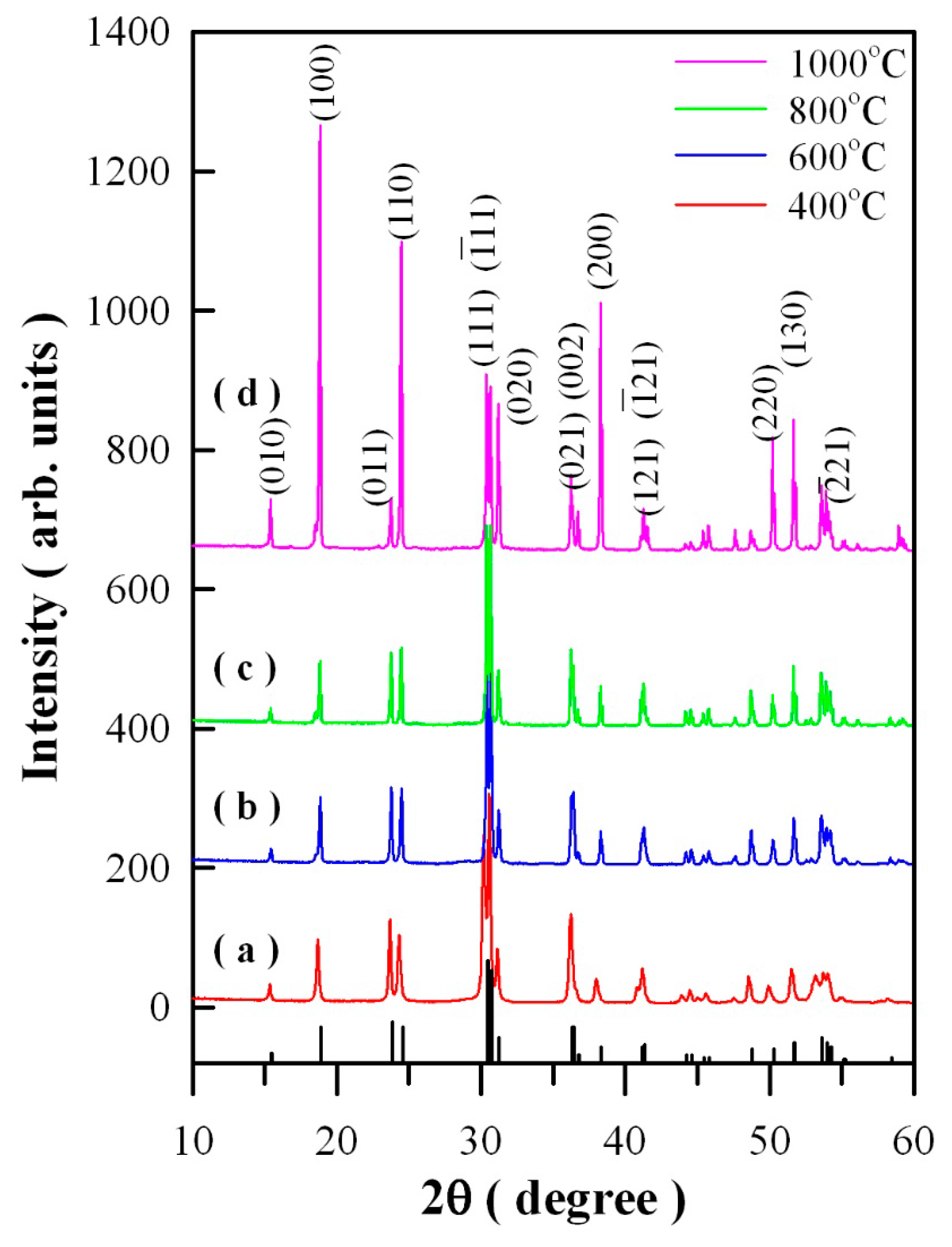
Figure 1 represents the XRD curves of Eu-doped ZnWO
4 precursors subjected to annealing at 400, 600, 800, and 1000 °C. In accordance with the standard XRD data for monoclinic ZnWO
4, the diffraction peaks at 15.36°, 18.68°, 23.68°, 24.32°, 31.10°, 37.98°, 49.90°, and 51.52° in
Figure 1 can be assigned to the reflections from the (010), (100), (011), (110), (020), (200), (220), and (130) planes of monoclinic ZnWO
4, respectively [
5,
25]. The vertical bars in
Figure 1 represent the XRD data of standard ZnWO
4 (JCPDS no. 15–0774) [
5]. Obviously, the peak at 30.40° is ascribed to the combined contributions from (111) and (−111) crystallographic planes since the two diffractions are located too closely [
2,
5]. For the same reason, the peak located at 36.20°can be ascribed to the contributions from the pair of planes (021) and (002), whereas the peak located at 41.24° can be ascribed to the contributions from the pair of planes (121) and (-121). As a result, the diffraction peaks of the four annealed samples can be indexed to the monoclinic phase ZnWO
4, indicating the crystalline nature of Eu-doped ZnWO
4 solids. Additionally, XRD analysis shows that the Eu-doped ZnWO
4 precursors exhibit a broad band before annealing and when the annealing temperature is lower than 400 °C. The reason is that the diffraction (crystallized) domain is low enough to enlarge the peaks. Temperature is a significant variable in the crystallization of materials, it often influences nucleation and crystal growth of the material. In general, the molecules in amorphous metal oxides do not have sufficient time to arrange in the most stable positions, and they become frozen in positions other than those of a regular crystal. Consequently, a sufficiently high temperature can convert the internal structure of the solid from amorphous to crystalline, which accompanies a drastic mass transfer and usually results in increasing density.
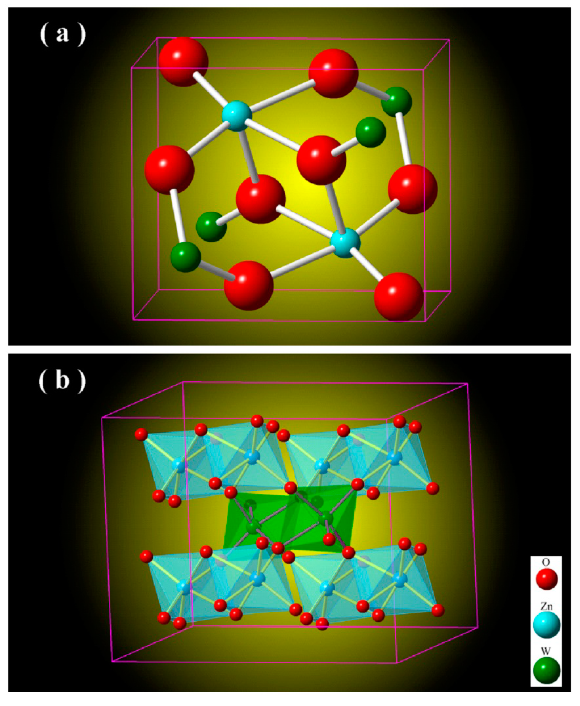
Figure 2 depicts the unit cell of monoclinic ZnWO
4 (a) and the metal-oxygen octahedrons in monoclinic ZnWO
4 (b). As shown in
Figure 2a, the unit cell of ZnWO
4 has two ZnWO
4 molecules, indicating that there are two Zn sites, two W sites and eight O sites in the unit cell of ZnWO
4. According to the data listed in JCPDS no. 15–0774 [
5], the lattice parameters of standard ZnWO
4 are
a = 0.4691 nm,
b = 0.5720 nm,
c = 0.4925 nm, and β = 90.64°. In crystalline ZnWO
4, each W
6+ ion is surrounded by six O ions to form a WO
6 octahedron, and each Zn
2+ ion is coordinated with six O ions to form a ZnO
6 octahedron. The ZnO
6 and WO
6 octahedrons in ZnWO
4 are represented in
Figure 2b. As shown in
Figure 2b, ZnWO
4 consists of zig-zag ZnO
6 and WO
6 chains. For example, one zig-zag ZnO
6 chain is made up of edge-sharing ZnO
6 octahedrons, and one zig-zag WO
6 chain is made up of edge-sharing WO
6 octahedrons [
26]. Moreover, each (ZnO
6–ZnO
6)
n chain is interlinked to four chains of (WO
6–WO
6)
n and vice versa. In the light of the crystal structures shown in
Figure 2, we can understand why there is no lattice expansion upon Eu doping of ZnWO
4. Shannon gave a value of 74 pm for a 6-fold coordination which is observed in the Zn tungstate. However, the ionic radii mismatch between Zn and Eu does not give any change in the cell parameters probably due to the weak Eu doping amount [
27]. Obviously, six coordinated W
6+ sites (
r = 60 pm) are too small for Eu
3+ to occupy. Thus, the lattice expansion in Eu-doped ZnWO
4 grains can be neglected when the doping concentration of is 5 mol % only.
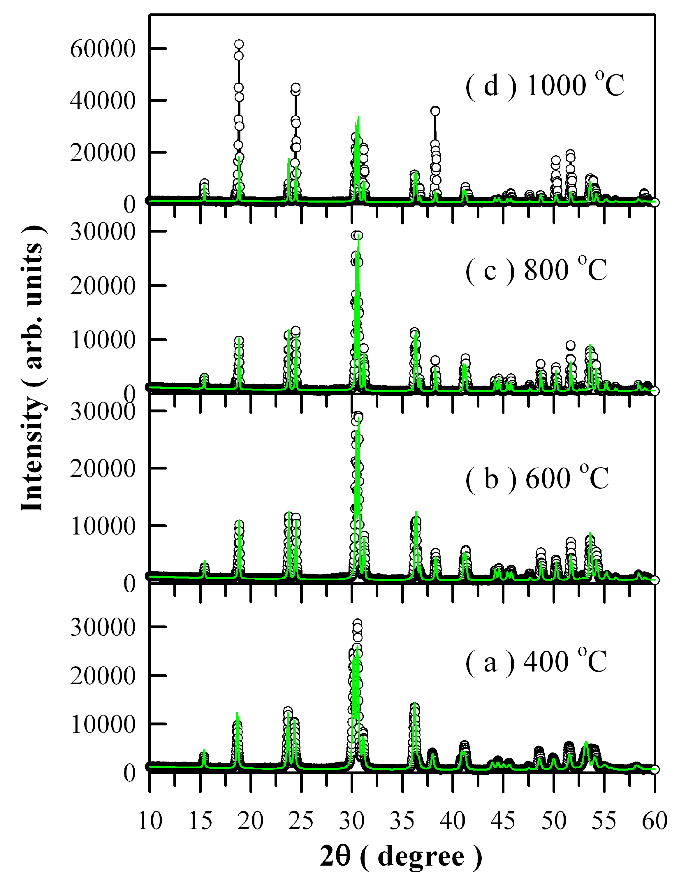
Figure 3 illustrates the Rietveld diffractograms of Eu-doped ZnWO
4 precursors subjected to annealing at different temperatures. The raw XRD data are represented by the open circles, and the calculated Rietveld diffractograms are represented by the solid green lines in
Figure 3. [
21,
28]. It can be seen in
Figure 3 that the calculated Rietveld diffractograms agree very well with the XRD curves a, b, and c but not for d. In XRD curve d, the diffraction intensities of the (100), (110), and (220) planes deviate significantly from those of calculated ones. The lattice parameters calculated from the Rietveld refinement are listed in
Table 1. For the convenience of comparison, the lattice parameters of ZnWO
4 single crystals are listed in the last row in
Table 1. For example, the calculated lattice parameters are
a = 0.4724 nm,
b = 0.5725 nm,
c = 0.4943 nm, and β = 90.9546° for Eu-doped ZnWO
4 precursors subjected to annealing at 400 °C. The calculated errors are ±0.0003 nm for the lattice lengths and ±0.0005° for β.
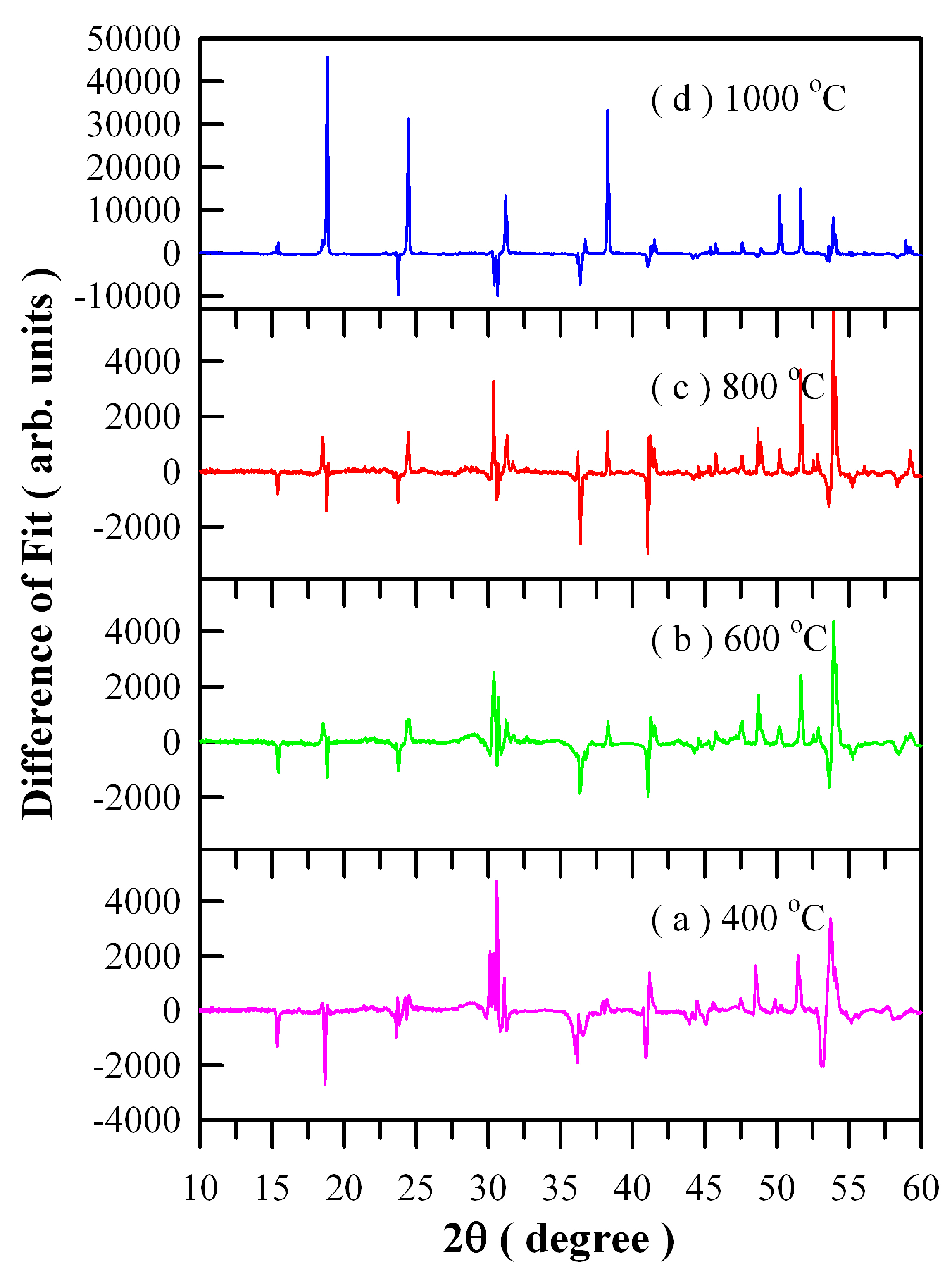
Figure 4 illustrates the differences between experimental and calculated XRD data of Eu-doped ZnWO
4 precursors subjected to annealing at different temperatures: (a) 400 °C; (b) 600 °C; (c) 800 °C; and (d) 1000 °C. It can be seen in
Figure 4 that good fit can be achieved for the three samples annealed at 400, 600, and 800 °C. However, it is surprising to observe a very bad fit for the 1000 °C annealed sample whereas the XRD data is correct. We are not sure what happens to the sample, and further investigation is required.
3.2. SEM Characterization of Eu-Doped ZnWO4
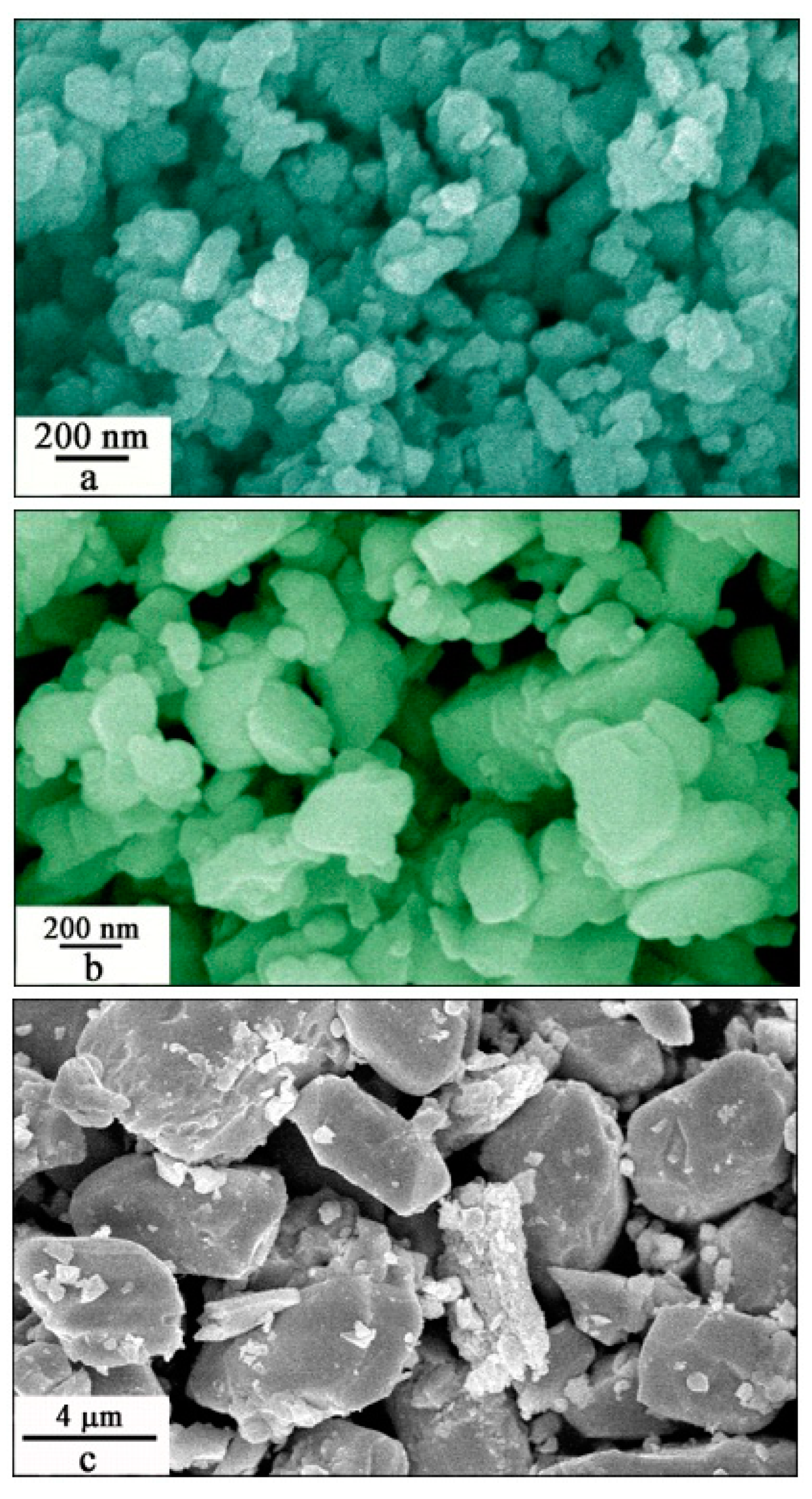
Figure 5 shows the SEM micrographs of Eu-doped ZnWO
4 precursors subjected to annealing at 400, 600, 800, and 1000 °C. As shown in
Figure 5a, the Eu-doped ZnWO
4 grains exhibit irregular shapes. According to crystal growth theory, the equilibrium shape of a crystal is determined by the Gibbs free energy, and the condition for minimization of the Gibbs free energy of a crystal formed at a constant volume is reduced to the minimization of surface energy. This is the Wullf’s theorem. The equilibrium shape of a liquid droplet is evidently a sphere. The case of a crystal is more complicated as the latter is confined by crystal faces with different crystallographic orientations which have different specific surface energies. This means that the surface energy depends on the crystallographic orientations, and the formation of non-spherical ZnWO
4 grains is therefore thermodynamically favorable. Obviously, the average particle size of the ZnWO
4 grains is about 80 nm, the standard deviation of the particle size distribution is calculated to be 30 nm. In principle, these ZnWO
4 grains can grow bigger if the annealing temperature gets higher. Indeed,
Figure 5b depicts that bigger Eu-doped ZnWO
4 grains are resulted as the thermal annealing temperature is raised to 600 °C. It can be seen in
Figure 5b that the ZnWO
4 grains are irregular in shape with their particle sizes in the range of 80–800 nm. The average particle size of the ZnWO
4 grains is about 400 nm with the standard deviation of the particle size distribution of about 190 nm. We can see that the Eu-doped ZnWO
4 grains are in the nanometer scale when the annealing temperature is 600 °C or less.
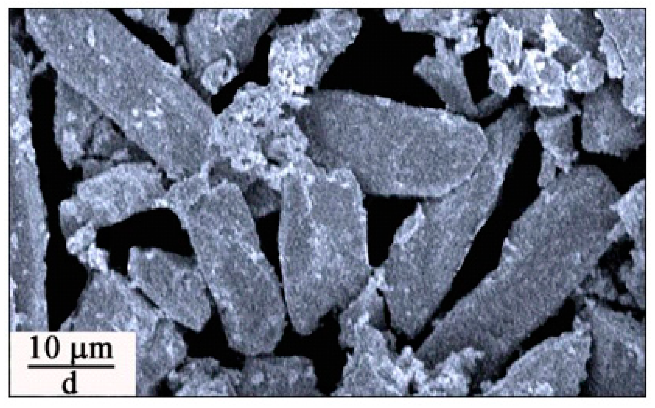
Figure 5c shows that the micrometer sized ZnWO
4 grains are resulted when the annealing temperature is elevated to 800 °C. The particle size of ZnWO
4 grains ranges from 2 to 8 μm. The mean value of the particle sizes is about 4 μm with the standard deviation of the the distribution of 2 μm. Finally, these ZnWO
4 grains can continue their growth if the annealing temperature is increased further.
Figure 5d shows that the lengths of ZnWO
4 grains are increased to about 20 μm when the annealing temperature is elevated to 1000 °C. In particular, these ZnWO
4 grains are rod-like with their aspect ratio ranging from 2 to 3. Overall, the micrographs in
Figure 5 have demonstrated that the control of annealing temperature has significant impacts on both the particle size and the morphology of ZnWO
4 grains. The annealing temperature dependent particle size and morphology of Eu-doped ZnWO
4 can generate significant effects on their surface area and surface defects, which in turn lead to dramatic changes in the optical absorption and emissions of Eu-doped ZnWO
4.
The power of solid-state annealing is the change in Gibbs free energy (or chemical potential energy) of the collections of ZnWO4 grains. The minimization of Gibbs free energy creates material transfer between particles through grain boundaries. Therefore, annealing any solid state crystalline material to sufficient temperatures will enable Oswald ripening, i.e., larger grains grow bigger at the expense of smaller grains. The growth of smaller grains to larger ones would reduce the specific surface areas due to the reduction in particle numbers and the elimination in pores, which in turn lead to the deduction in surface defect concentration. Since both the grain-boundary diffusion and the volume diffusion rely heavily upon temperature, the control of temperature is critically important to the particle size and morphology of Eu-doped ZnWO4. For example, grain growth typically goes exponentially with temperature but only linearly with time at a given temperature. This is the generalized Arrhenius’ plot. That is the reason why ZnWO4 grains grow bigger and bigger when the annealing temperature gets higher and higher.
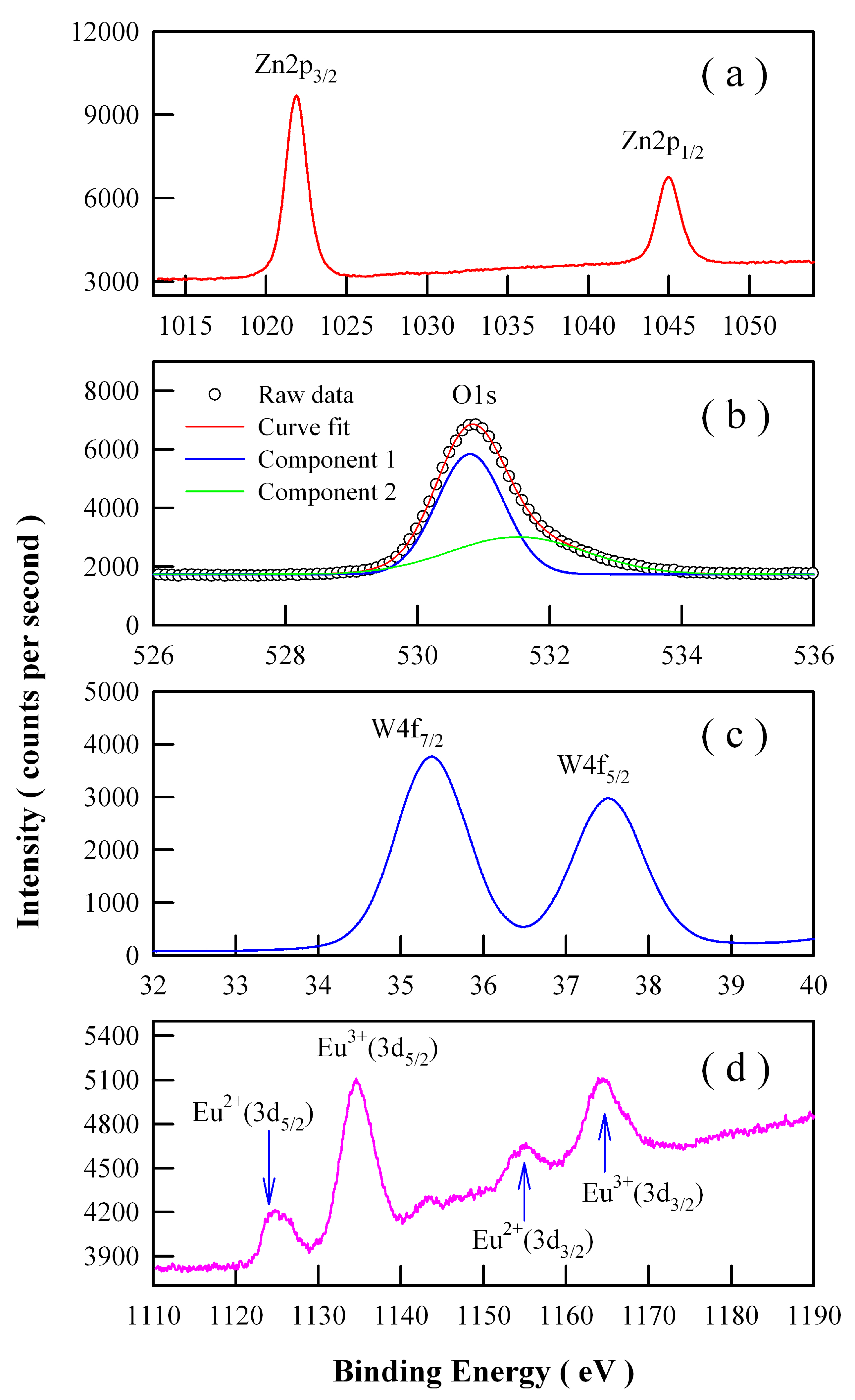
3.4. X-ray Photoelectron Spectroscopic Characterization of Eu-Doped ZnWO4 Grains
Ionic Eu can exist in the valence state of Eu
3+ or Eu
2+ [
21,
22]. Therefore, we have to explore the chemical states of Eu ions in the phosphors. High-resolution XPS spectra are shown in
Figure 7 for Zn 2p, O 1s, W 4f, and Eu 3d in Eu-doped ZnWO
4 nanoparticles derived by annealing the precursor at 400 °C. As can be seen clearly in
Figure 7a, the XPS peaks of Zn 2p
3/2 at 1021.88 eV and Zn 2p
1/2 at 1044.98 eV correspond to the typical Zn
2+ oxidation states in ZnWO
4 nanoparticles. As shown in
Figure 7b, the peak of the XPS spectrum of O 1s is located at 530.88 eV. Detailed analysis shows that this spectrum has two components. The first component is peaked at 530.80 nm and the second component is peaked at 531.52 nm. The second component, which is centered at 531.52 eV, can be attributed to the oxygen vacancies in ZnWO
4.
Figure 7c indicates that the XPS peaks of W 4f
7/2 at 35.38 eV and W 4f
5/2 at 37.48 eV can be assigned to W 4f
7/2 and W 4f
5/2, respectively. In particular,
Figure 7d reveals that Eu ions exist in ZnWO
4 grains in the form of mixed valence states. As shown in
Figure 7d, four peaks can be identified at 1124.78, 1134.58, 1155.18, and 1163.88 eV. According to previous reports, the first two peaks in
Figure 7d can be assigned to Eu
2+ (3d
5/2) and Eu
3+ (3d
5/2) core-levels whilst the last two peaks in
Figure 7d can be assigned to Eu
2+ (3d
3/2) and Eu
3+ (3d
3/2) core-levels, respectively [
31,
32]. The binding energy of Eu
2+(3d
5/2) is 30.4 eV lower than that of Eu
2+ (3d
3/2), and the binding energy of Eu
3+(3d
5/2) is 29.3 eV lower than that of Eu
3+(3d
3/2). The area ratios of the XPS signals are approximately 1.48:5.15:1.00:3.37 for Eu
2+(3d
5/2): Eu
3+(3d
5/2): Eu
2+(3d
3/2): Eu
3+ (3d
3/2). With a standard of Eu
2+ doped ZnWO
4 (doping level 1 mol %), we measured its high-resolution XPS spectrum of Eu 3d
3/2 and Eu 3d
5/2. The peak areas of Eu
2+ (3d
5/2) and Eu
2+ (3d
3/2) are obtained by area integration of the spectrum. The comparison of the peak areas of Eu
2+ (3d
3/2) and Eu
2+ (3d
5/2) in
Figure 7d with those of the reference sample, the concentration of Eu
2+ in the Eu-doped ZnWO
4 nanoparticles can be determined. In this way, the concentration of Eu
2+ in Eu-doped ZnWO
4 nanoparticles is derived to be 0.9 mol %, leaving the concentration of Eu
3+ in Eu-doped ZnWO
4 to be 4.1 mol %. Consequently, the data in
Figure 7d point out the presence of Eu
2+ and Eu
3+ in ZnWO
4 nanoparticles, although Eu
3+ ions are the only doping source in the starting materials. Consequently, a fraction of Eu
3+ ions must be self-reduced to Eu
2+ ions [
22].
It is known that oxygen vacancy (V
O) can be easily produced in the lattice of ZnWO
4 in the crystal growth phase. As one V
O is formed in ZnWO
4, one positively charged V
O is left in the lattice. In the meanwhile, one negatively charged oxygen species is released into the lattice in order to keep the lattice neutral. When the negatively charged oxygen species diffuses randomly in the lattice, it donates its electrons with the liberation of oxygen out of the lattice. This process can be described by Equation (1)
In this way, the vacancy V
O would act as a donor of electrons. Eu
3+ ion can be reduced to Eu
2+ by capturing the released electron. A detailed discussion on the self-reduction of Eu
3+ to Eu
2+ can be found elsewhere [
22], and this process can be described by Equation (2)
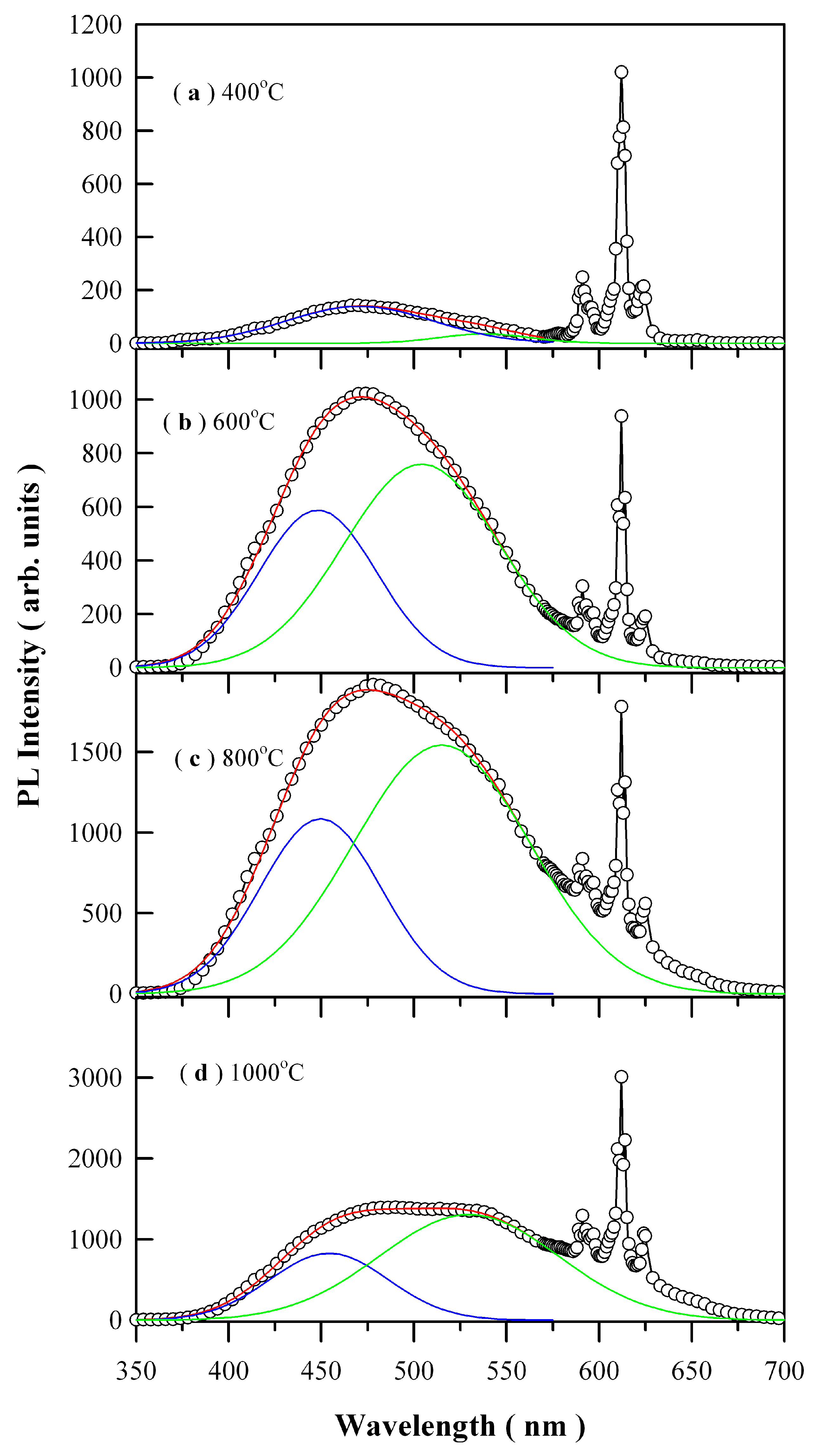
3.5. Photoluminescence Spectra of Eu-Doped ZnWO4 Phosphors
Figure 8 depicts the PL spectra of Eu-doped ZnWO
4 precursors subjected to annealing at 400, 600, 800, and 1000 °C. The open circles in
Figure 8 represent the raw PL data. The general feature in
Figure 8 is that each PL spectrum is composed of a broad PL band centered at about 480 nm and the three sharp emissions peaking at 590, 612, and 625 nm, respectively. It is known that trivalent rare-earth ions are characterized by an electronic structure consisting of an unfilled inner 4f shell and outer filled 5s and 5p shells. When these trivalent rare-earths are present in a solid, the effects of the crystalline field are a small perturbation on the 4f states because of the shielding of the outer electron shells. Since the interaction with host is weak, their emission spectrum is nearly independent of host lattice. Such kind of host independence was evidenced by the characteristic emissions of Eu
3+, Tb
3+, and Dy
3+ in a variety of hosts [
21,
22,
24,
28,
29,
30,
33]. The other feature of trivalent rare-earth ions is that their 4f–4f transitions are parity forbidden. In the case of Eu
3+, the electric-dipole transitions between the
5D
0 and
7F
2 states of Eu
3+ ion are parity-forbidden although the much weaker magnetic dipole transition between
5D
0 and
7F
1 is allowed. In practice, however, it turns out that intra-configurational electric-dipole transitions are often dominant since even a small admixture with odd symmetry components to the electronic wave-function of 4f configuration causes significant changes in the transition probabilities and allows the electric-dipole transitions. Therefore, the dominant peak centered at about 612 nm in
Figure 8 can be attributed to the hypersensitive
5D
0→
7F
2 transition of Eu
3+ ions in ZnWO
4 lattice whereas the peak with low intensity at about 590 nm is assigned to the
5D
0→
7F
1 transition. It can be clearly seen that the peak intensity of the dominant electric-dipole transition is much larger than that of the magnetic dipole transition, demonstrating that Eu
3+ ion occupies non-centrosymmetric sites in the host lattice.
Each of the broad PL band in
Figure 8 can be decomposed into two Gaussian components according to Equation (3)
where
I (λ) is the PL intensity recorded at wavelength λ;
I1, λ
1 and
σ1 are the pre-exponential factor, mean value and standard derivation of the first Gaussian component, respectively. Meanwhile,
I2, λ
2, and
σ2 are the pre-exponential factor, mean value, and standard derivation of the second Gaussian component, respectively [
34]. For brevity, the first Gaussian component is denoted as the blue PL component whilst the second Gaussian component is denoted as the green PL component, which are represented by the solid blue curve and the solid green curve for each PL spectrum in
Figure 8, respectively. The red curve in each panel is the sum of the two components. The fitting parameters of the two-component Gaussian decomposition of the PL spectra are listed in
Table 2. The most striking feature in
Figure 8 is the coexistence of the blue PL component and green PL component, which suggests the presence of two kinds of distinctly different luminescence centers in ZnWO
4. The second most striking feature in
Figure 8 is that both the peak positions and the PL intensities of the two PL components are annealing temperature dependent. For example, the peak position of the blue PL component varies in the range of 448.12 to 470.69 nm in the meanwhile the peak position of the green PL component varies in the range of 504.19 to 538.08 nm. Moreover, with respect to red emissions of Eu
3+ at 612 nm, the PL intensity of ZnWO
4 host increases gradually to its maximum as the annealing temperature increases from 400 through 600 to 800 °C, and then it turns its head down as the annealing temperature is increased further from 800 to 1000 °C. The annealing temperature dependent PL bears significance in defect engineering of the emissions from ZnWO
4 host. For instance, it can be employed to realize color tunable emissions if the blue emissions from ZnWO
4 host are combined to the red emissions from Eu
3+ ions.
The broad PL band from ZnWO
4 host is often attributed to the charge transfer between oxygen and tungsten ions in [WO
6]
6− molecular complex [
1]. However, such assignment is quite elusive for physicists. In the view of solid-state physics, the origins of PL can be classified into band edge emission and defect emission. Due to the large difference between the bandgap of ZnWO
4 (about 4 eV) and its emission energy (around 2.6 eV), we can exclude the possibility of band edge recombination as the candidate of the broadband emissions of ZnWO
4 grains. In actual cases, defect emissions often dominate the PL properties in diverse metal oxides such as HfO
2 [
35], Zn
5Mo
2O
11 [
28], SrAl
2O
4 [
36,
37], BaAl
2O
4 [
33], and ZnMO
4 [
38]. This also holds true for ZnWO
4 grains, where coordinatively unsaturated vacancies are active sites for luminescence. This feature allows us to assign the broad PL band peaking at about 480 nm to certain kinds of defects in ZnWO
4. The most common defects in ZnWO
4 include O, W, and Zn vacancies, which are likely candidates of the luminescence centers. Although the relation between the intrinsic defects and the luminescence centers in ZnWO
4 are not clearly identified yet, the PL spectra in
Figure 8 demonstrate that the PL properties of ZnWO
4 host are highly governed by the number and the kind of defects in ZnWO
4 lattice. The role of Eu
3+ doping is to provide the red emission so that tunable PL from blue to red can be realized by combining the blue-green emission from ZnWO
4 host with the red emission from Eu
3+ dopant. Without the red emission from Eu
3+ dopant, the emission color of ZnWO
4 host can be tuned only in the blue-green spectral regime. Instead of varying the concentration of Eu
3+ ions in ZnWO
4, this work shows how to harness the defect engineering in ZnWO
4 to achieve color tunable emissions even when the doping concentration is fixed.
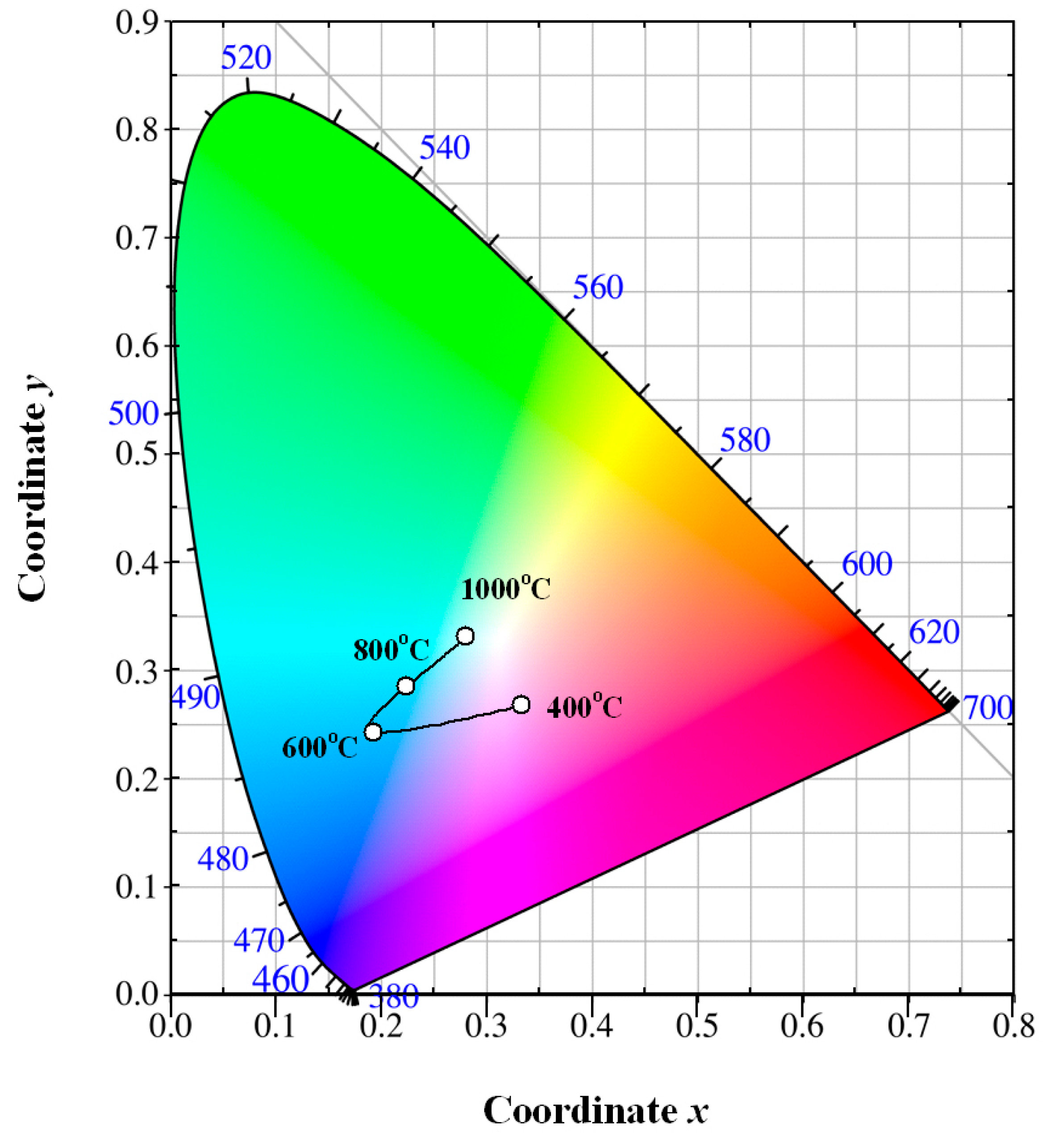
3.6. Color Coordinates of Eu-Doped ZnWO4
Once the PL spectrum of Eu-doped ZnWO
4 phosphors is modified by the control of annealing temperature, the perception color will be changed correspondingly. On the basis of the PL spectral data, the chromaticity coordinates can be calculated in the Commission Internationale de L’Eclairage (CIE) 1931 XYZ color space [
28].
Figure 9 depicts the evolution of the luminescence color of Eu-doped ZnWO
4 precursors with annealing temperature. The solid line in
Figure 9 is for eye guidance only. After annealing at 400 °C for 2 h, the luminescence color of the phosphor is purplish pink with its color coordinates of (0.333, 267). After annealing at 600 °C for 2 h, the luminescence color of the phosphor is changed to greenish blue with its color coordinates of (0.193, 0.242). After annealing at 800 °C for 2 h, the luminescence color of the phosphor is also greenish blue with its color coordinates of (0.223, 0.284). After annealing at 1000 °C for 2 h, the luminescence color of the phosphor is white with its color coordinates of (0.280, 0.331). Among the four phosphors, the chromaticity coordinates (0.280, 0.331) are very close to the achromatic point whose coordinates are (0.333, 0.333). It is known that white light-emitting phosphors are critically important in solid state lighting industry. There is reason to believe that white light emissions can be achieved in Eu-doped ZnWO
4 phosphors by fine adjustment of the annealing temperature. Our work demonstrates that color tunable emissions can be achieved by thermal annealing the phosphors at different temperatures. Rather than controlling the doping concentration of Eu
3+ ion [
5,
8,
13,
14,
15], the color tunable PL from Eu-doped ZnWO
4 is realized by engineering the intrinsic defect emissions from ZnWO
4 lattice through variations of annealing temperature. Therefore, the strategy of tuning the emission color of Eu-doped ZnWO
4 turns out to be a strategy on how to control the intrinsic defects in ZnWO
4 in an environmentally friendly, cost-effective, scalable, and controllable manner.
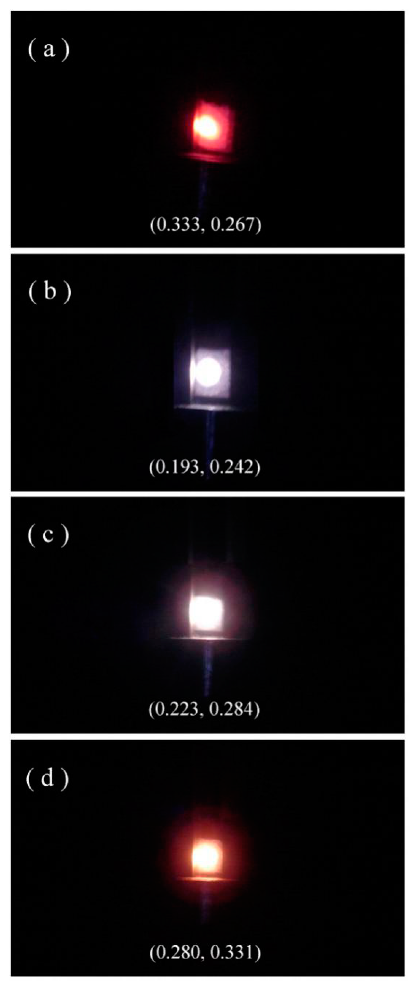
The annealing temperature dependent PL suggests the feasibility to tune the PL color of Eu-doped ZnWO
4.
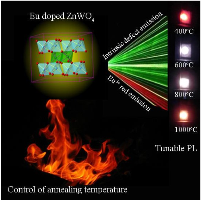
Figure 10 shows the luminescence photos of Eu-doped ZnWO
4 precursors subjected to annealing at 400, 600, 800, and 1000 °C. The calculated color coordinates are displayed in each photo. It is obvious in
Figure 10 that the luminescence color of Eu-doped ZnWO
4 depends on the annealing temperature. In our case, tunable color is realized by mixing the blue emissions from ZnWO
4 lattice with the red emissions from Eu
3+ ions. Such a change in the luminescence color can be understood when we refer to the dramatic changes in the broadband PL intensity as the annealing temperature increases from 400 to 1000 °C. In a similar way, Zhai et al. reported that white light-emitting can be obtained by combining the bluish emission of tungstate group with the characteristic emission of Eu
3+ and Dy
3+ [
15]. With the method described earlier [
21], the correlated color temperatures are calculated to be 5437, 50,758, 18,053, and 8437 K for the four Eu-doped ZnWO
4 phosphors which were annealed at 400, 600, 800, and 1000 °C, respectively. Our work demonstrates that the emission color of Eu-doped ZnWO
4 can be manipulated over a significant range through variations of the annealing temperature.
3.7. Electronic Structures of Perfect ZnWO4 and Defect-Containing ZnWO4
Many kinds of defects are present in practical solids. Examples of the intrinsic defects in ZnWO
4 include vacancies (O vacancy, Zn vacancy, W vacancy), interstitials (O interstitial, Zn interstitial, W interstitial) and antisites (O antisite, Zn antisite, W antisite), etc. After having considered the high formation energies of antisites, the three kinds of vacancies are the most probable intrinsic defects in ZnWO
4 with sufficiently high population. Even in the absence of doping agent Eu
3+ ions, O, W, and Zn vacancies occur naturally in the lattice of ZnWO
4 at any given temperature up to the melting point of the material. A Kröger–Vink representation of Schottky defect formation in ZnWO
4 can be described by Equation (4)
It can be seen in Equation (4) that V
O can act as electron trap since it is positively charged. Similarly, both Zn vacancy and W vacancy can act as hole trap since they are negatively charged. As discussed above, intrinsic defects in ZnWO
4 have played important roles in the broadband emissions. Therefore, the electronic structures of intrinsic defects in ZnWO
4 are critically important to understand the absorption and luminescent properties of ZnWO
4. Density functional calculations can be reliably applicable to the electronic structure calculations for a variety of materials [
21,
23,
24,
30]. In the framework of GGA+U, we performed electronic structure calculations for perfect ZnWO
4 and defect-containing ZnWO
4 by defining U
5d = 10 eV for W.
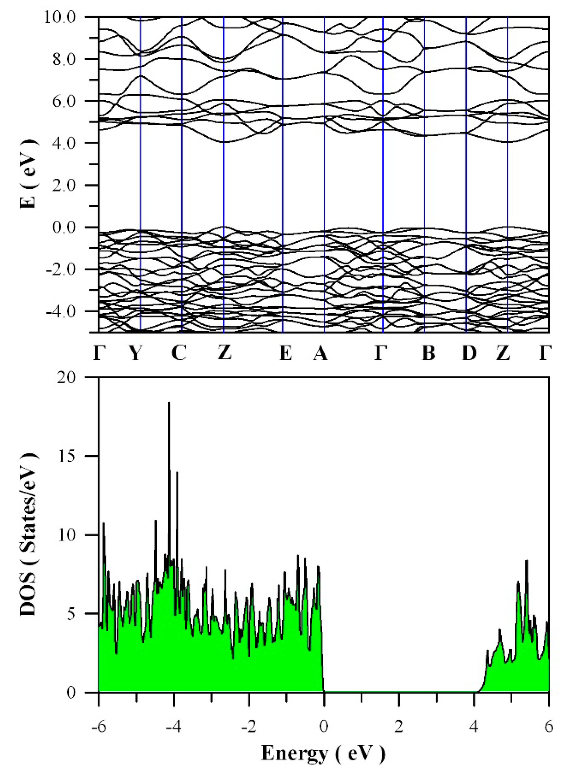
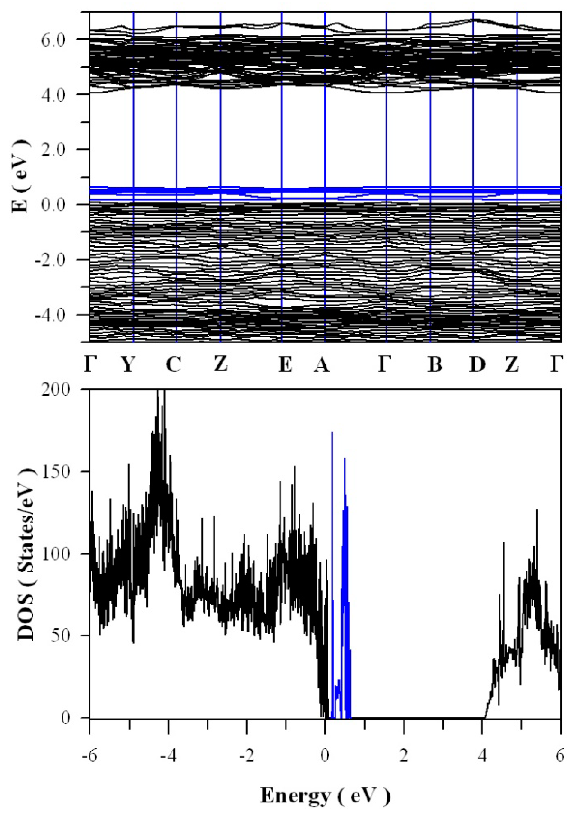
Figure 11 presents the calculated band structures and density of states of perfect ZnWO
4. As shown in
Figure 11a, both the maximum of valence band (VB) and the minimum of conduction band (CB) are located at Z point, confirming that ZnWO
4 is a semiconductor with direct bandgap. The bandgap value is derived to be 4.04 eV. Moreover, it can be seen that some bands at the bottom of CB are not flat, which is the typical character of a semiconductor. In principle, the bandgap value can also be calculated from the density of states of defect-free ZnWO
4. On the basis of the density of states shown in
Figure 11b, the calculated bandgap is 4.04 eV, too, for defect-free ZnWO
4. The most prominent feature in
Figure 11b is that the bandgap of ZnWO
4 is free of any impurity energy levels. The second most prominent feature in
Figure 11b is that perfect ZnWO
4 possesses remarkably sharp band edges. On the basis of ab initio study, Kalinko et al. reported that ZnWO
4 is a direct semiconductor with its bandgap value of around 2.31 eV [
39]. In our GGA+U calculations, the bandgap values are 2.64, 2.87, 3.12, 3.41, 3.72, and 4.04 eV when U
5d = 0, 2, 4, 6, 8, 10 eV for W, respectively. So U
5d = 10 eV is the best value to fit the experimental bandgap data. By measuring the diffuse reflectance spectrum of ZnWO
4 film coated on quartz substrate, Zhao et al. reported that the experimental bandgap of the ZnWO
4 film was about 4.01 eV [
40]. It can be seen that our derived bandgap value is in reasonable agreement with the experimental bandgap value reported by Zhao et al.
V
O is one of the most fundamental defects in ZnWO
4, it influences many physical properties of the material such as charge trapping and recombination. Therefore, detailed knowledge of the electronic structures of V
O is essential in understanding the PL of ZnWO
4. In order to model V
O in ZnWO
4, we built a 2 × 2 × 2 super cell which contains 64 O sites, 16 W sites and 16 Zn sites. After one O site was removed from this super cell, oxygen deficient ZnWO
4 is resulted with the atomic concentration of V
O in ZnWO
4 up to 1 at %. For simplicity, this oxygen deficient ZnWO
4 is denoted as ZnWO
4−δ where δ = 0.0625.
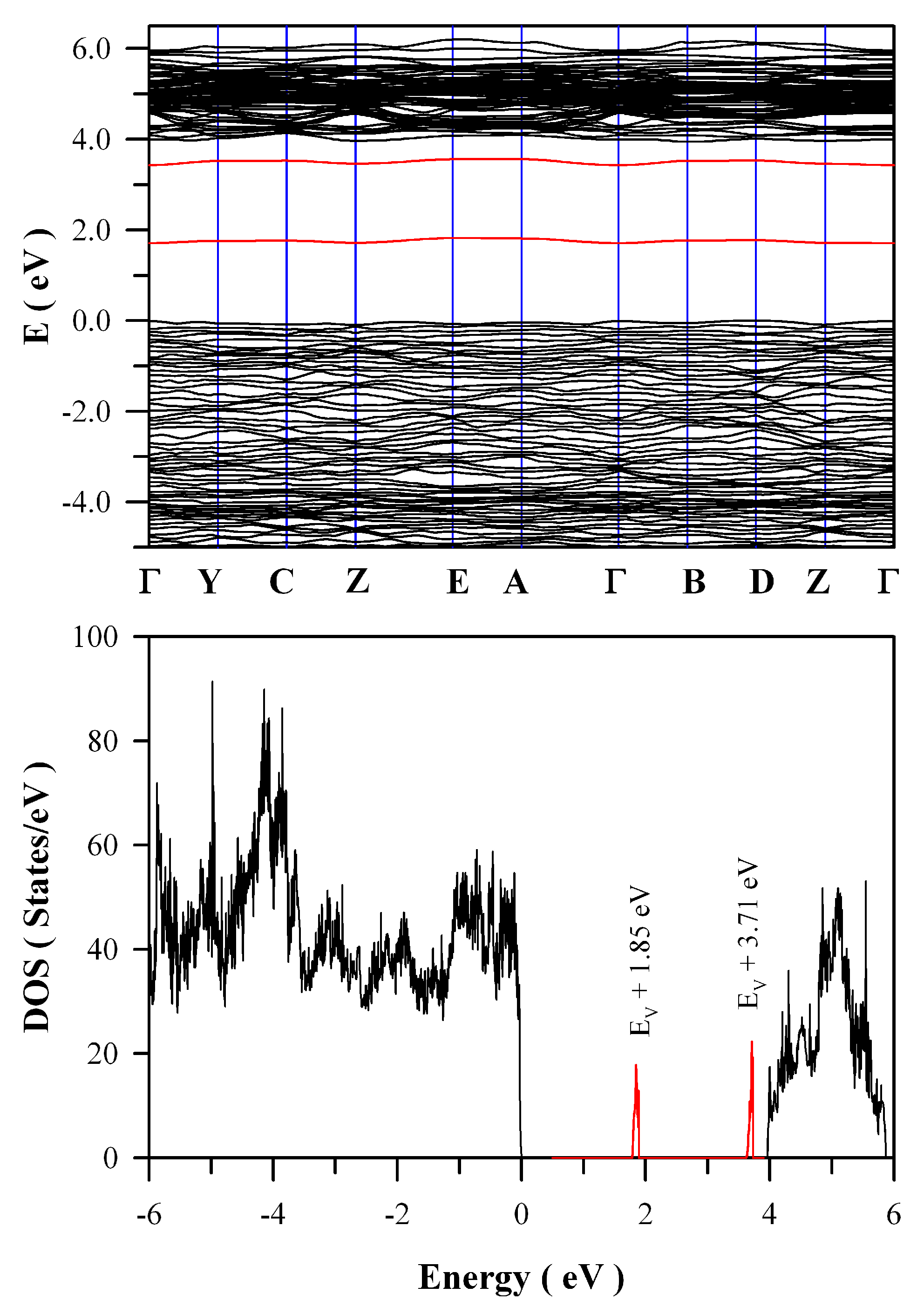
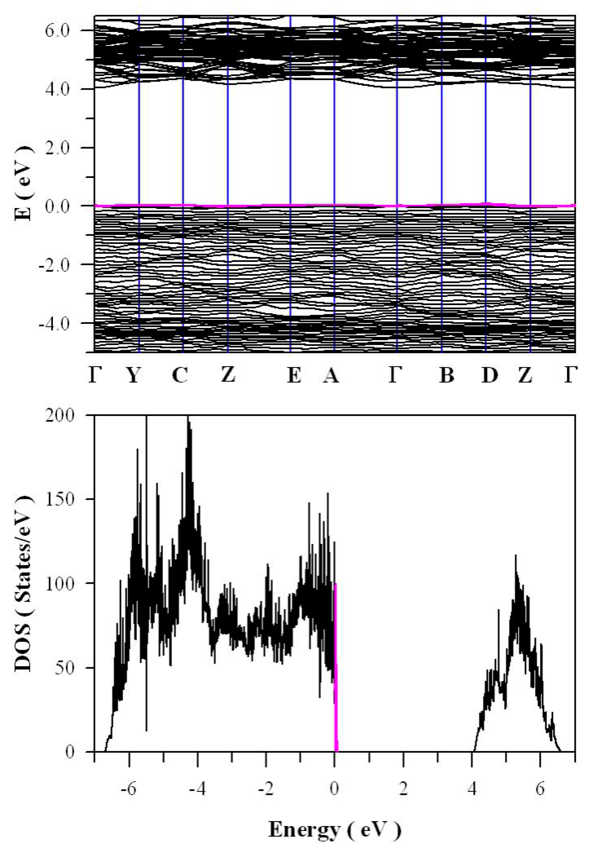
Figure 12 represents the calculated band structures and density of states of oxygen deficient ZnWO
4. As shown in
Figure 12a, the calculated bandgap of V
O bearing ZnWO
4 is 4.04 eV when U
5d = 10 eV for W. The most prominent feature in
Figure 12 is that V
O can introduce two defect energy levels in the bandgap of ZnWO
4, one of which is located at E
V + 1.85 eV whilst the other is located at E
V + 3.71 eV. The two defect energy levels are clearly marked in red, as shown
Figure 12b. Since it is positively charged, V
O can act as electron trap sites as well as luminescence center as they do in HfO
2 [
35].
Besides V
O, tungsten vacancy (V
W) can be also present in ZnWO
4. Understanding the electronic structures of V
W quantitatively is important for developing this family of materials for potential applications, which include emission color tunable phosphors. In order to model V
W in ZnWO
4, we built a 2 × 2 × 2 super cell which contains 64 O sites, 16 W sites and 16 Zn sites. After one W site was removed from this super cell, tungsten deficient ZnWO
4 is resulted with the atomic concentration of V
W in ZnWO
4 up to 1 at %. For simplicity, this tungsten deficient ZnWO
4 is denoted as ZnW
1−δO
4 where δ = 0.0625.
Figure 13 shows the calculated band structures and density of states of tungsten deficient ZnWO
4. As can be seen in
Figure 13a, the bandgap remains direct with the value of 4.05 eV. In contrast to the clean bandgap of perfect ZnWO
4, the bandgap of tungsten deficient ZnWO
4 contains a lot of defect energy levels. It can be seen clearly in
Figure 13b that the defect energy levels created by V
W span from E
V + 0.1 eV to E
V + 0.7 eV, where the V
W introduced defect energy levels are marked in blue. The peak of V
W created band is located at E
V + 0.62 eV. Since it is negatively charged, V
W can act as hole trap sites as well as luminescence center.
As the other typical defect, zinc vacancy (V
Zn) can be present in ZnWO
4. Being negatively charged, V
Zn can also act as charge carrier traps and luminescence centers. Therefore, we have to take the Zn defect states into account in order to understand the defect emissions from ZnWO
4. In order to model V
Zn in ZnWO
4, we built a 2 × 2 × 2 super cell which contains 64 O sites, 16 W sites, and 16 Zn sites. After one zinc site was removed from this super cell, zinc deficient ZnWO
4 is resulted with the atomic concentration of V
Zn in ZnWO
4 lattice up to 1 at %. For simplicity, this tungsten deficient ZnWO
4 is denoted as Zn
1−δWO
4 where δ = 0.0625.
Figure 14 shows the calculated band structures and density of states of zinc deficient ZnWO
4. As marked in pink in
Figure 14a, there are some zinc defect energy levels in the bandgap of ZnWO
4, but they are very close to the top of VB (<0.1 eV). From a perfect Zn site, the Kröger–Vink notation for the defect reactions of V
Zn in ZnWO
4 can be described by Equation (5)
In Equation (5), the masses, sites and charges are balanced for the intrinsic defects. Equation (5) indicates that the creation of a VZn from a zinc site in ZnWO4 yields one negatively charged defect VZn and one positively charged zinc interstitial defect. The creation of a VZn is quite similar to the p-type doping silicon with phosphorus since positive charges are released into the host lattice. Obviously, the negatively charged VZn can work as an acceptor with the capability of trapping holes in ZnWO4. It is interesting to note that the acceptor levels in the forbidden band are closely packed above the VB of ZnWO4. This phenomenon can be understood in the light of weak interaction between the zinc interstitial defect and the negatively charged VZn. The low ionization energy for the release a zinc interstitial defect is responsible for are closed packed zinc defect energy levels just above the VB of ZnWO4.
Belong to 4f–5d transition, Eu
2+ doped nanomaterials generally show a broad PL band ranging from ultraviolet through visible to infrared regime. However, Eu
2+ doped ZnWO
4 grains exhibit no extra PL band in the visible range when compared to undoped ZnWO
4 grains. We recorded the PL spectrum of Eu
2+ doped ZnWO
4 with the 325 nm excitation wavelength.
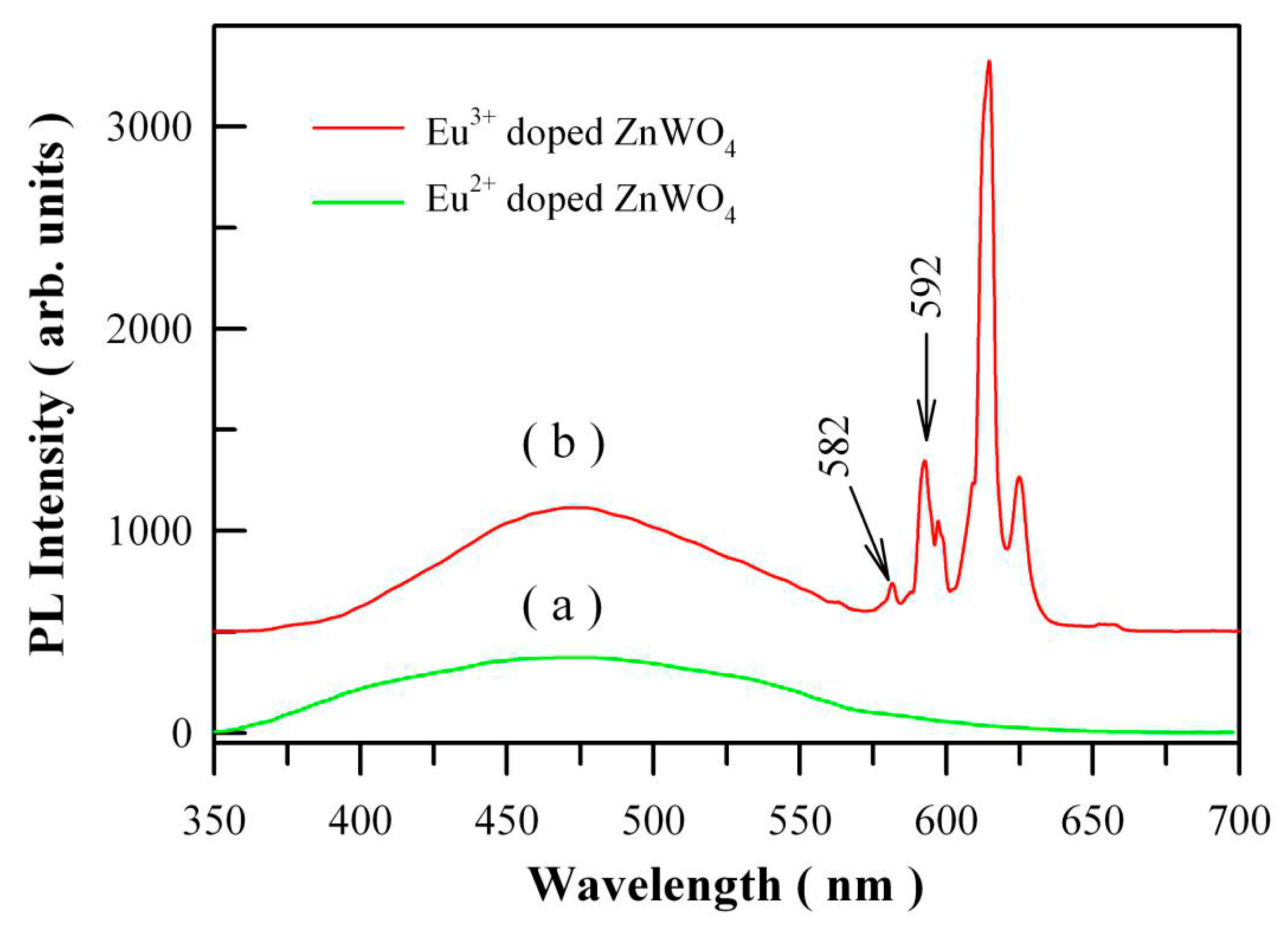
Figure 15a shows the PL spectrum of Eu
2+ doped ZnWO
4 with the doping concentration of 1 mol %. When compared to the PL spectrum of Eu
3+ doped ZnWO
4 as shown in
Figure 15b, we can see that the presence of Eu
2+ does not introduce an extra PL band in the visible spectral regime. It is possibly due to the low amount of Eu
2+ ions in ZnWO
4. Further exploration is required to study the Eu
2+ emission in ZnWO
4 host. As for Eu
3+ doped ZnWO
4, the 4f electrons of the dopant are sufficiently localized to form multiple atomic-like states in the bandgap of ZnWO
4 due to the shielded 4f–shell. Since the DFT calculations are one-electron theory, the DFT with GGA scheme fails to accurately predict the multi-electron properties of Eu
3+ ions in ZnWO
4. Consequently, neither the energies of J multiplets of Eu
3+ ions (
7F
J, where
J = 0–6) in the ground state nor the energy levels in the excited state (
5D
0) of Eu
3+ ions can be deduced correctly from the DFT calculations. That is why we did not model the defect energy levels of Eu
3+ in ZnWO
4. Fortunately, both the energy levels of Eu
3+ in ground state and in excited state vary by only a small amount in different hosts. Thus, the energy levels of
7F
J and
5D
0 of Eu
3+ in ZnWO
4 can be determined by making use of the experimentally obtained energies for Eu
3+. The only exception is that the exact location of the lowest energy level of Eu
3+ (
7F
0) is unknown for the case of ZnWO
4. Additionally, the PL spectrum of Eu
3+ doped ZnWO
4 with a better resolution is shown in
Figure 15b. The excitation wavelength is 325 nm. It can be seen that the
5D
0→
7F
0 emission peak is located at about 582 nm although it is very low in intensity.
3.8. Defect Absorption of Eu-Doped ZnWO4
Optical absorption spectroscopy is one of the most significant experimental techniques to investigate the optical absorption of defects in semiconducting crystals. In semiconductors, photoexcitation often results in strong band-edge absorption, and optical absorption of defects in semiconducting crystals is often observed in the ultraviolet and visible spectral regime.
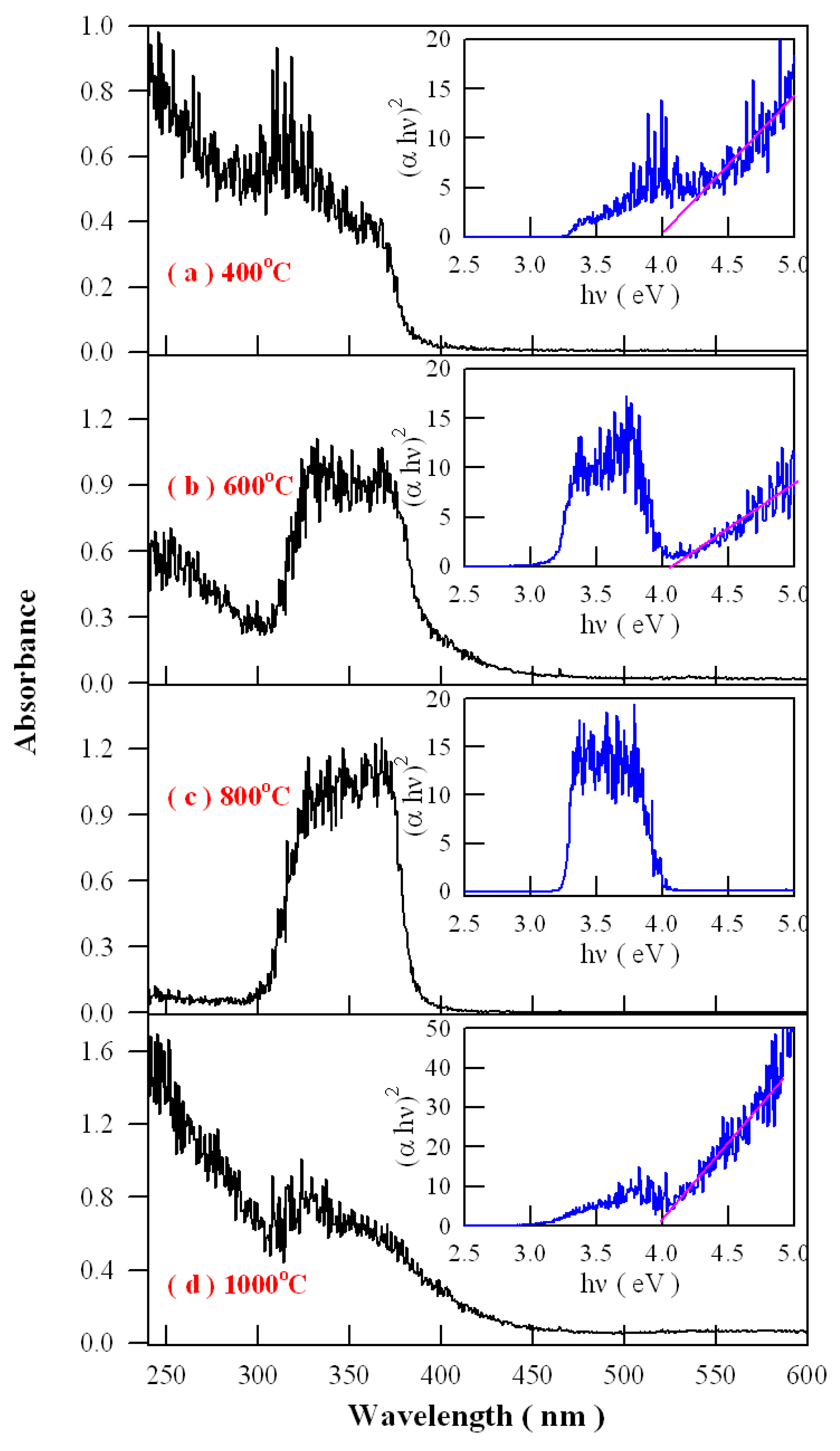
Figure 16 represents the absorption spectra of Eu-doped ZnWO
4 precursors subjected to annealing at 400, 600, 800, and 1000 °C. As shown
Figure 16, an extra absorption band appears in the range of 300–400 nm with its center at around 350 nm. Being superposed the strong absorption of ZnWO
4 host, this absorption band is relatively weak in intensity as the annealing temperature is 400 °C, but it becomes stronger in intensity as the annealing temperature gets higher to 600 °C. When the annealing temperature is raised to 800 °C, the extra absorption band reaches its maximum, as shown in
Figure 16c. After that, this extra absorption band starts to lose its intensity when the annealing temperature is elevated further to 1000 °C. It is noted that the peak position of this absorption band does not shift with the annealing temperature although dramatic changes in the absorption intensity are recorded. Alongside with the absorption spectra, the insets in
Figure 16 illustrate the Tauc plots of the Eu-doped ZnWO
4 phosphors. The optical bandgaps of the Eu-doped ZnWO
4 phosphors, as indicated by the solid pink lines in the Tauc plots, are very close to 4.0 eV. Additionally, the defect absorptions can be seen clearly in the Tauc plots, too. As compared to others, the absorbance behavior of the curve at 800 °C is particular because the defect absorption band is so strong that the band-edge absorption is severely depressed. This case suggests that the defect concentration in ZnWO
4 reaches the maximum. Therefore, the data in
Figure 16 indicate that the defect concentration in ZnWO
4 phosphors increases with the annealing temperature until it reaches to maximum at 800 °C. Then the defect concentration in ZnWO
4 phosphors decreases as the annealing temperature increases further to 1000 °C.
Analysis of the intensity, width, and shape of the extra absorption band sometimes can yield a lot of information about the defect absorption in ZnWO
4. The defect absorption band is centered at about 350 nm (3.54 eV). It is clear that the intensity of the extra absorption band heavily depends on the annealing temperature. When referred to defect energy levels of V
O shown in
Figure 12, it is found that this absorption band coincides in energy with the transition from VB to the defect level of V
O at E
V + 3.71 eV. Moreover, for condensed matter and solids, the shape of absorption bands are determined by the density of states of the initial state and the density of states of the final states that are involved into electronic transitions. The comparison of the extra absorption band in
Figure 16 with the calculated DOS in
Figure 11 clearly discloses that this absorption band is due to electronic transition from VB to the deep donor level of V
O at E
V + 3.71 eV. Consequently, the data in
Figure 16 give evidence of V
O related defect absorption at about 350 nm.
Thermal annealing is the process of subjecting a substance to the action of heat, but without melting or fusion, for the purpose of causing some change in its physical or chemical constitution. In our case, thermal annealing generates numerous defects in ZnWO
4. It is well established that the population density of V
O in a solid increases quickly with the increase in annealing temperature according to Equation (6)
where
n is the population density of V
O in the solid,
A is the proportionality constant,
QV is activation energy for vacancy formation of V
O in the host,
T is the absolute temperature in Kelvin, and k is the Boltzmann constant [
22]. It can be seen from Equation (6) that high population density of V
O can be easily created in ZnWO
4 when the annealing temperature is elevated. For this reason, the V
O related absorption band gets stronger in intensity after having been annealed at a higher temperature. The higher the annealing temperature is, the more V
O is produced in ZnWO
4, which result in stronger defect absorption. It is worthwhile to note that the population density in Equation (6) stands for the population density of volume defects in ZnWO
4 but not the population density of surface defects on ZnWO
4 grains. Actually, the surface defects cannot be neglected in our case. As shown in
Figure 5, the mean particle size of ZnWO
4 grains increases from 80 nm to 20 μm as the annealing temperature increase from 400 to 1000 °C. At a given volume, the surface area of ZnWO
4 grains derived at 1000 °C is about 1/4000 of the surface area of ZnWO
4 grains derived at 400 °C. It is well known that the growth of larger grains would reduce the surface areas by particle number reduction and pore elimination, which inevitably leads to the decrease in the surface defect concentration. Obviously, the increase in the volume defect concentration will be mediated by the rapid decrease in the surface defect concentration as ZnWO
4 grains grow bigger and bigger. It is anticipated that the increase in the volume defect is outnumbered by the decrease in surface defects at specific temperature, beyond which the total number of defects in ZnWO
4 starts to decline. This is the reason why the defect absorption in
Figure 16d is decreased significantly with respect to that in
Figure 16c. The annealing temperature dependent defect absorption provides a novel avenue to the control of defect emissions in ZnWO
4.
3.9. Possible Mechanism of Tunable PL from Eu-Doped ZnWO4
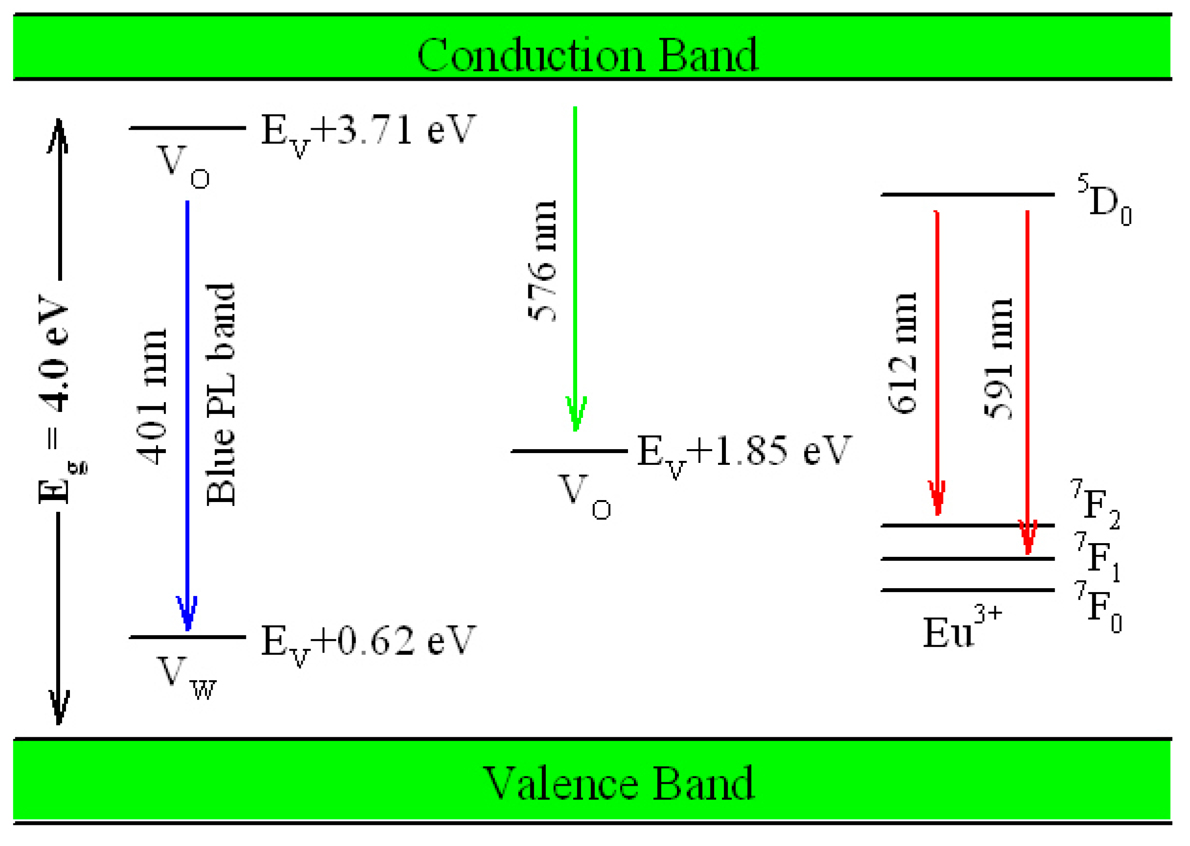
Figure 17 illustrates the possible mechanism of tunable PL from Eu-doped ZnWO
4. As displayed in
Figure 17, the bandgap value of ZnWO
4 is assumed to be 4.0 eV, the V
O introduced defect energy levels are located at E
V + 1.85 eV and E
V + 3.71 eV. V
O is positively charged thus it can capture electrons. Meanwhile, V
W introduced defect energy level is located at E
V + 0.62 eV. V
W is negatively charged thus it can capture holes. Under the UV excitation, electrons are pumped into the conduction band (CB) of ZnWO
4, leaving holes in the VB of ZnWO
4. This process is accompanied with strong band-edge absorption, which is shown by the Tauc plots in
Figure 16. In addition to the band-edge absorption, defect absorption can sometimes be recorded, too. According to
Figure 17, the transition from VB to the defect energy level of V
O at E
V + 3.71 eV should yield a defect absorption band peaking at 335 nm. Indeed, this extra absorption band is evidenced by the extra absorption spectra in
Figure 16. After photoexcitation, the photo-generated electrons and holes will be relaxed via diverse paths. The first kind of radiative recombination is the electrons trapped by V
O at E
V + 3.71 eV to recombine with the holes trapped by V
W at E
V + 0.62 eV, resulting in the blue PL band peaking at around 428 nm (2.90 eV). The second kind of radiative recombination is the electrons in CB to recombine with the positively charged V
O at E
V + 1.85 eV, yielding the green PL band peaking at around 576 nm (2.15 eV). From this point of view, both the blue component and the green component of the broadband PL spectrum are readily explained. Obviously both the intrinsic defects V
O and V
W are involved into the radiative recombinations. When compared to the energies of the blue and the green PL bands in
Figure 8, our predicted emission energies of the defect emissions roughly agree to the experimental values. The differences between the predicted emission energies in
Figure 17 and the actual emission energies in
Figure 8 rest on the fact that it is hard to exactly and reliably determine the defect energy levels with DFT calculation due to the limitations in semilocal approximations to DFT. The third kind of radiative recombination is the electrons in the excited state
5D
0 of Eu
3+ to recombine radiatively with the holes in its ground states
7F
1,2, leading to the characteristic emissions peaking at 591 and 612 nm.
In the light of the mechanism proposed in
Figure 17, we can understand the color tunable PL from Eu-doped ZnWO
4. Standard color-mixing uses red, green and blue emissions that are adjusted to deliver the entire range of the color spectrum. In our case, tunable PL from Eu-doped ZnWO
4 uses color mixing of the red emissions from extrinsic defects Eu
3+ ions with the bluish emissions from intrinsic defects in ZnWO
4 lattice. Since the interaction of rare earth dopants with host is weak, their emission spectra of trivalent rare earth dopants are nearly independent of host lattice. Consequently, how to adjust the output of the bluish emissions from ZnWO
4 lattice has become the task of controlling the intrinsic defect emissions in ZnWO
4. As disclosed by our DFT calculation and optical absorption, the bluish emissions from ZnWO
4 lattice are originated from intrinsic defects V
O and V
W, whose population densities can be tuned by carefully controlling the annealing temperature. This is the reason why the output of the bluish emissions from ZnWO
4 host can be tuned through the control of annealing temperature. When compared to the strategy of dopant concentration control, our approach is uniquely positioned to adjust the intrinsic defects in ZnWO
4 lattice by the fine control of annealing temperature. This strategy provides new capability of tuning the emissions from rare earth doped ZnWO
4 even when the rare earth doping concentration is fixed.
3.10. Time-Resolved PL Spectra of Eu-Doped ZnWO4
In order to gain more physical insight on the defect emissions in ZnWO
4, we studied the time-resolved PL behaviors of Eu-doped ZnWO
4.
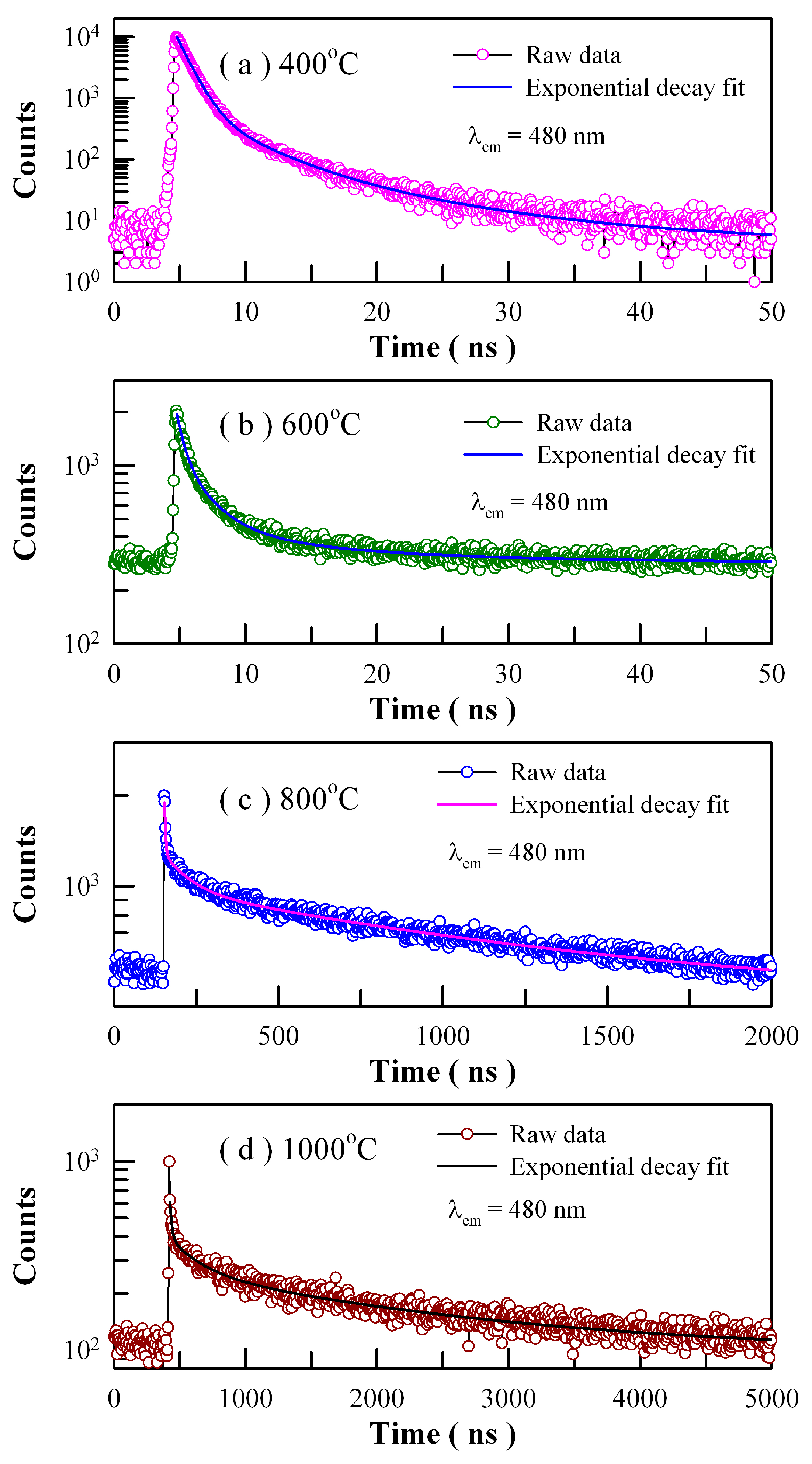
Figure 18 depicts the time-resolved PL spectra of Eu-doped ZnWO
4 precursors subjected to annealing at 400, 600, 800, and 1000 °C. The excitation wavelength is 375 nm and the detection wavelength is 480 nm. The raw data are represented by the circles, and the fitted curves are represented by the solid lines represent. It is found that each decay curve in
Figure 18 can be fitted with one triple exponential function as described in Equation (7)
where
I(
t) stands for the PL intensity at time
t,
A is the baseline,
Bi is the ith pre-exponential factor of the decay components, and
τi is the ith decay time component (
i = 1–3). The fitting parameters of the time-resolved PL spectra are listed in
Table 3. The parameter χ
2 in
Table 3 represents the goodness of fit, and the average lifetime <
τ> is calculated by using the Equation (8) [
41].
These parameters bear important information on the kinetics of carrier recombination. For example, the decay time constants are
τ1 = 0.92 ns,
τ2 = 3.52 ns and
τ3 = 10.47 ns with <
τ> = 2.25 ns for Eu-doped ZnWO
4 precursors subjected to annealing at 400 °C. It is noted that
τ1 is at the limit of the measurement capability of the instrument and therefore it merely represents the order of the short decay time constant [
21,
28,
37,
38]. The coexistence of
τ2 and
τ3 for each annealed sample suggests the presence of two different radiative recombination paths in ZnWO
4. Indeed, the two radiative recombination paths are determined in
Figure 8 and
Figure 17. Alternatively, we have to note that the average PL lifetimes in
Table 3 are particle size dependent. As can be seen in
Table 3, the average lifetimes of first two samples (i.e., ZnWO
4 nanocrystals) are less than 10 ns whereas those of the last two samples (i.e., ZnWO
4 microcrystals) range from 1.19 μs to 1.77 μs. The average lifetime of ZnWO
4 microcrystals is about 100 times longer than that of ZnWO
4 nanocrystals, indicating the dramatic reduction in the non-radiative recombination paths in ZnWO
4 microcrystals. When compared to nanocrystals, ZnWO
4 microcrystals are characteristic of much less surface defects due to their reduced surface area. As is well known, these surface defects may act as PL quenching centers. Thus, the reduction in the surface defects is responsible for the prolonged average lifetimes of ZnWO
4 microcrystals.
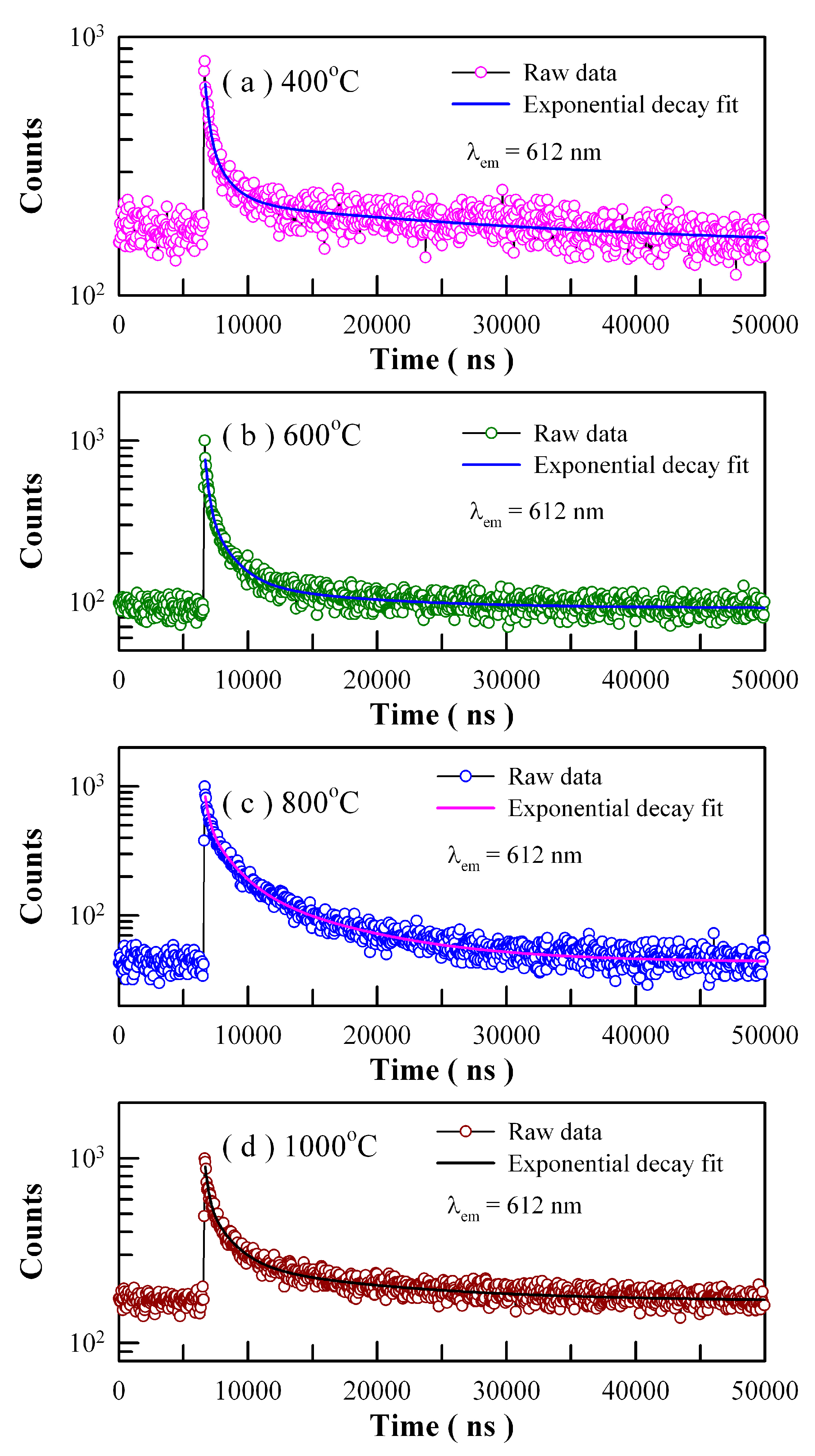
The PL lifetimes of Eu emissions are usually longer than nanoseconds. In some cases, it can be extended into microseconds and even milliseconds.
Figure 19 shows the time-resolved PL spectra of Eu-doped ZnWO
4 precursors subjected to annealing at 400, 600, 800, and 1000 °C. The excitation wavelength is 375 nm and the detection wavelength is 612 nm. Circles in
Figure 19 represent the experiment data while the solid lines represent the fitted curves. It is found that each PL decay curve in
Figure 19 can be fitted with one triple exponential function. The fitting parameters of the time-resolved PL spectra of Eu-doped ZnWO
4 phosphors are listed in
Table 4. According to Equation (8), the average PL lifetimes of Eu
3+ emissions at 612 nm are calculated to be 24.28, 5.20, 5.77 and 8.86 µs for the Eu-doped ZnWO
4 precursors subjected to annealing at 400, 600, 800, and 1000 °C, respectively. As documented in the literature, Wang et al. reported that the average PL lifetime of Pr
3+ doped ZnWO
4 at 607 nm was 5.40 µs [
41]. It is clear that the average PL lifetimes of Eu
3+ emissions and Pr
3+ emissions in ZnWO
4 are at the same order of magnitude. Since Eu is supposed to be located in a unique crystallographic site, namely Zn, we tried to fit each of the PL decay curves in
Figure 19 with a unique exponential function. The decay time constants are derived to be 1.879, 1.548, 3.544, and 2.995 μs for the samples annealed at 400, 600, 800, and 1000 °C, respectively. In the meanwhile, the values of goodness of fit are 1.536, 1.808, 2.617, and 2.208 for the samples annealed at 400, 600, 800, and 1000 °C, respectively. When compared to the fit with the sum of three exponential functions, the fit with a unique exponential function gives a much clearer picture of the underlying physical processes but suffers more from statistical reliability. It is obvious that much more work is needed in order to interpret the time-resolved PL spectra in
Figure 19.


