ZnO Nanowire Networks as Photoanode Model Systems for Photoelectrochemical Applications


 and
and 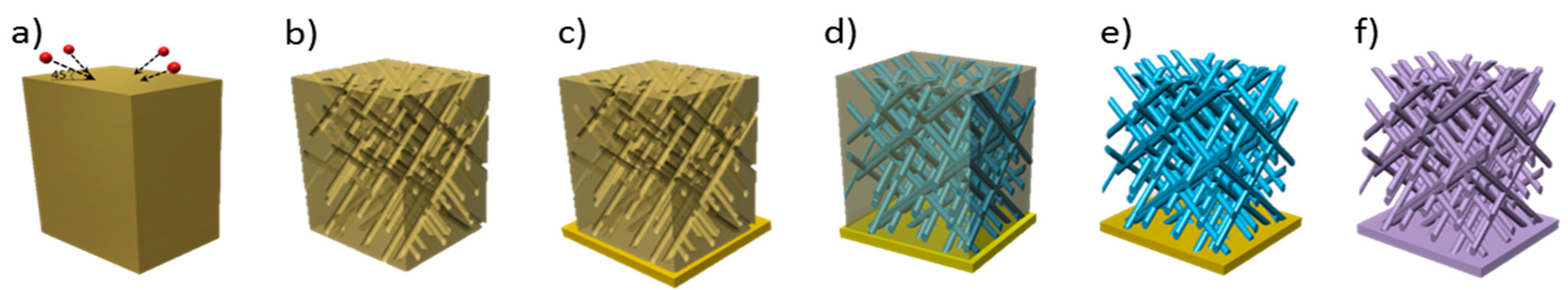
Abstract
1. Introduction
2. Materials and Methods
2.1. Membrane Fabrication
2.2. ZnO Electrodeposition
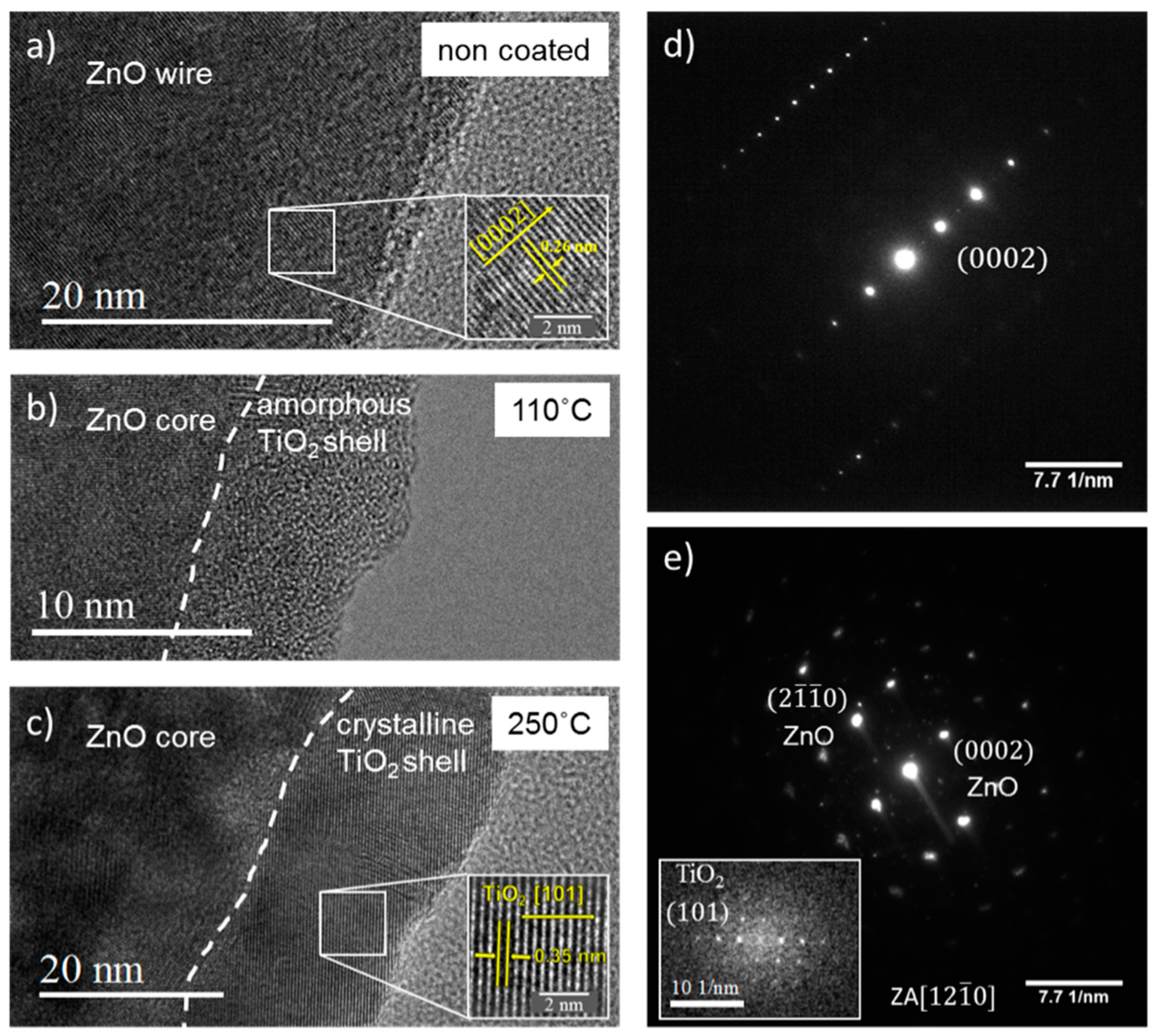
2.3. TiO2 Atomic Layer Deposition
2.4. Photoelectrochemical Measurements
2.5. Sample Characterization
3. Results
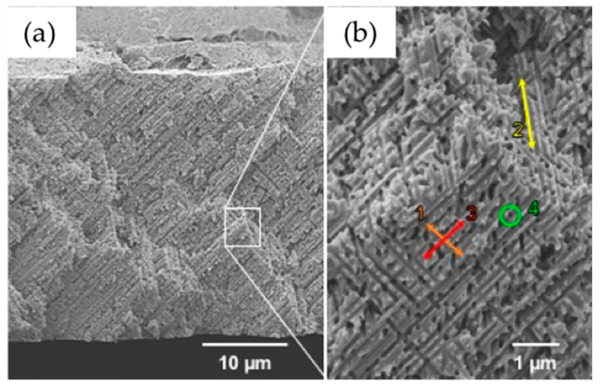
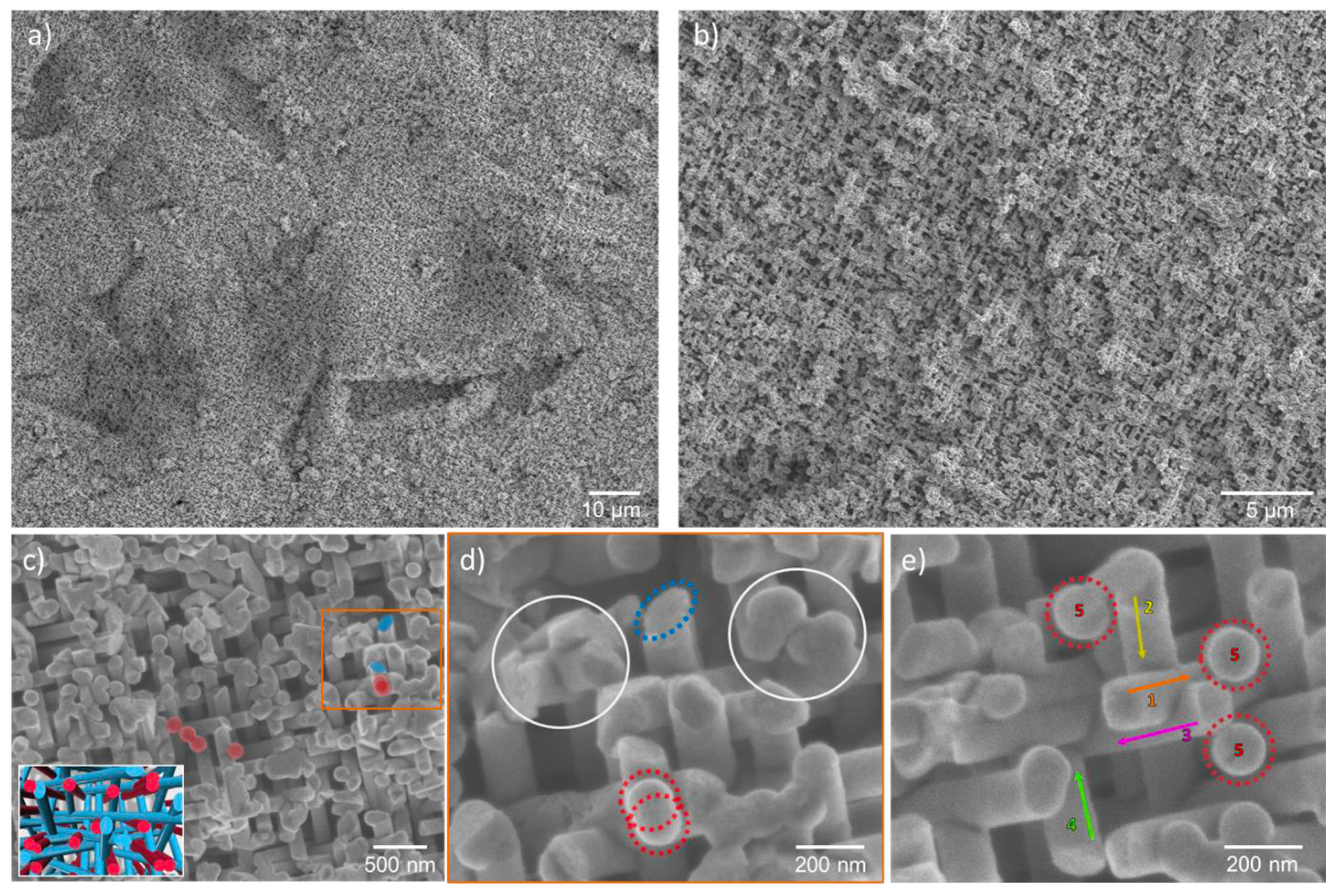
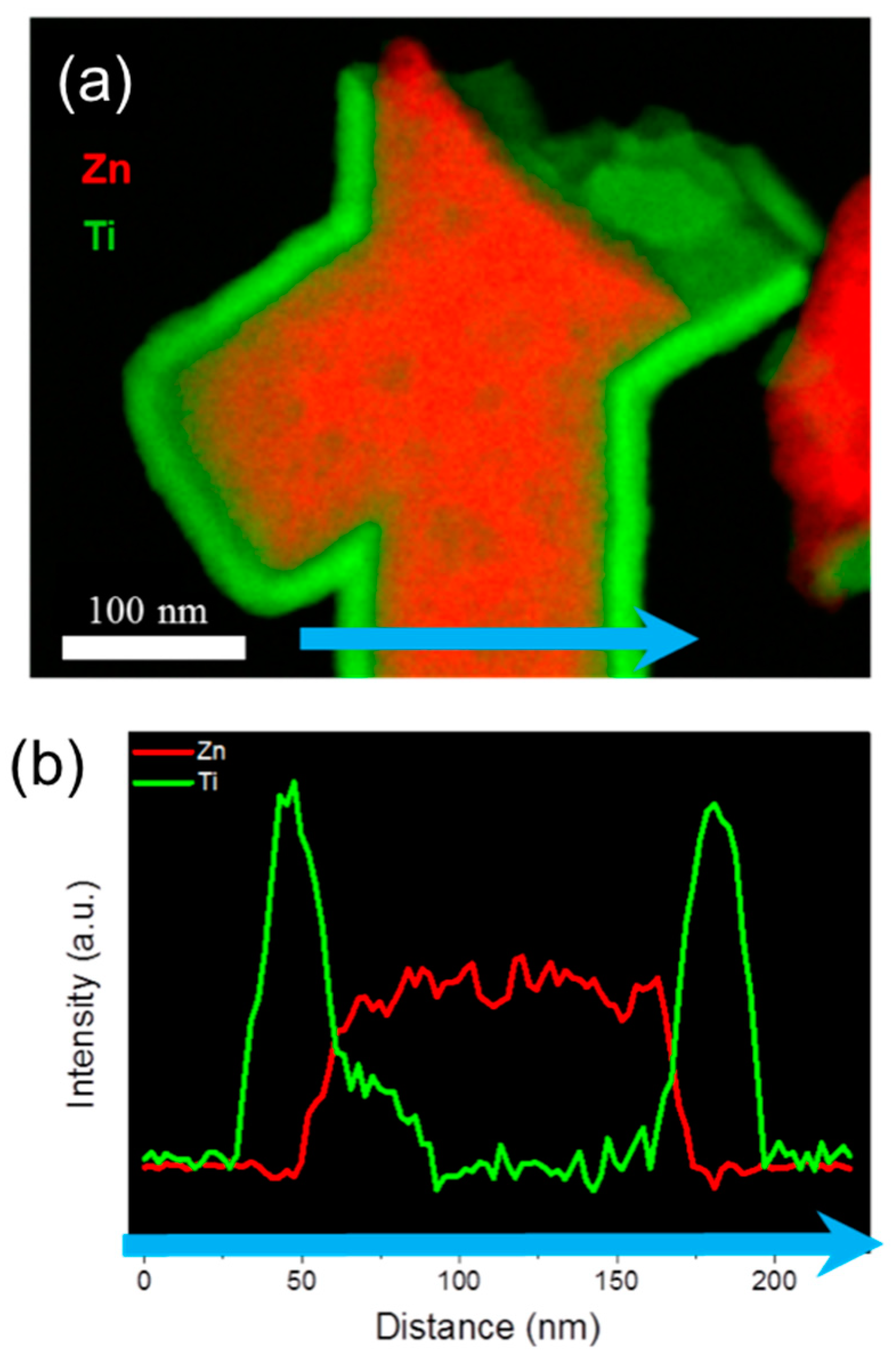
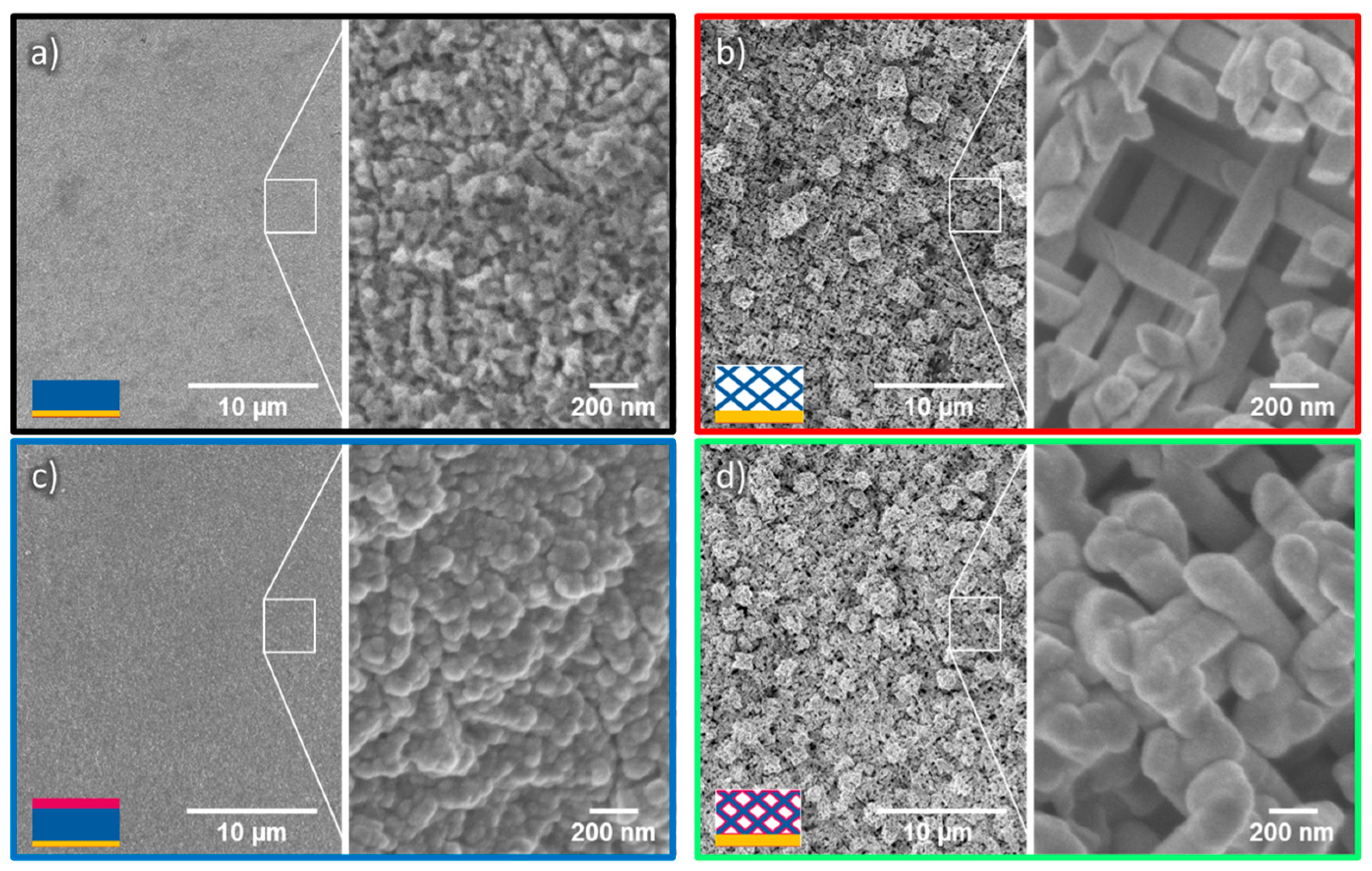
3.1. Network Analysis
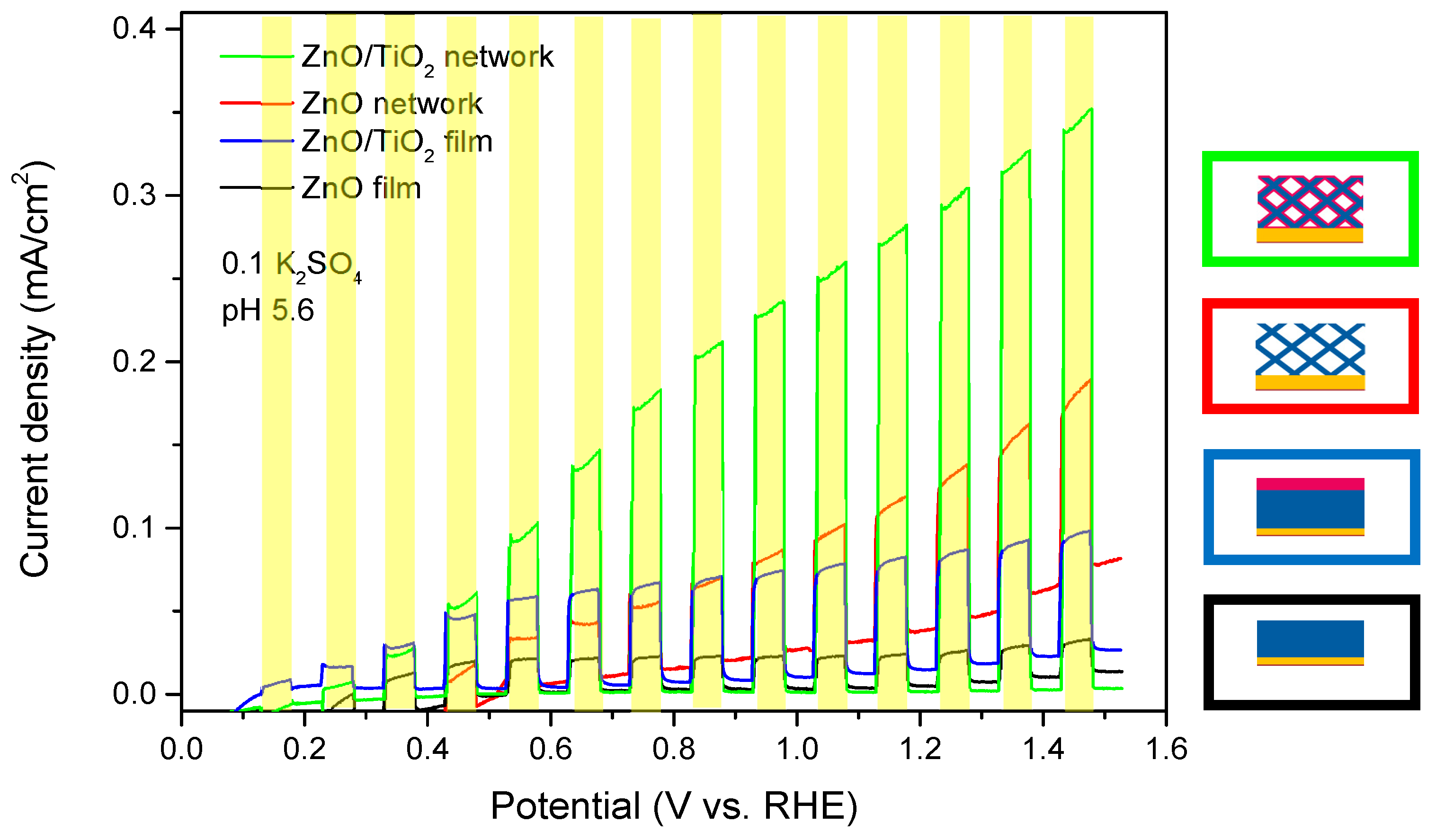
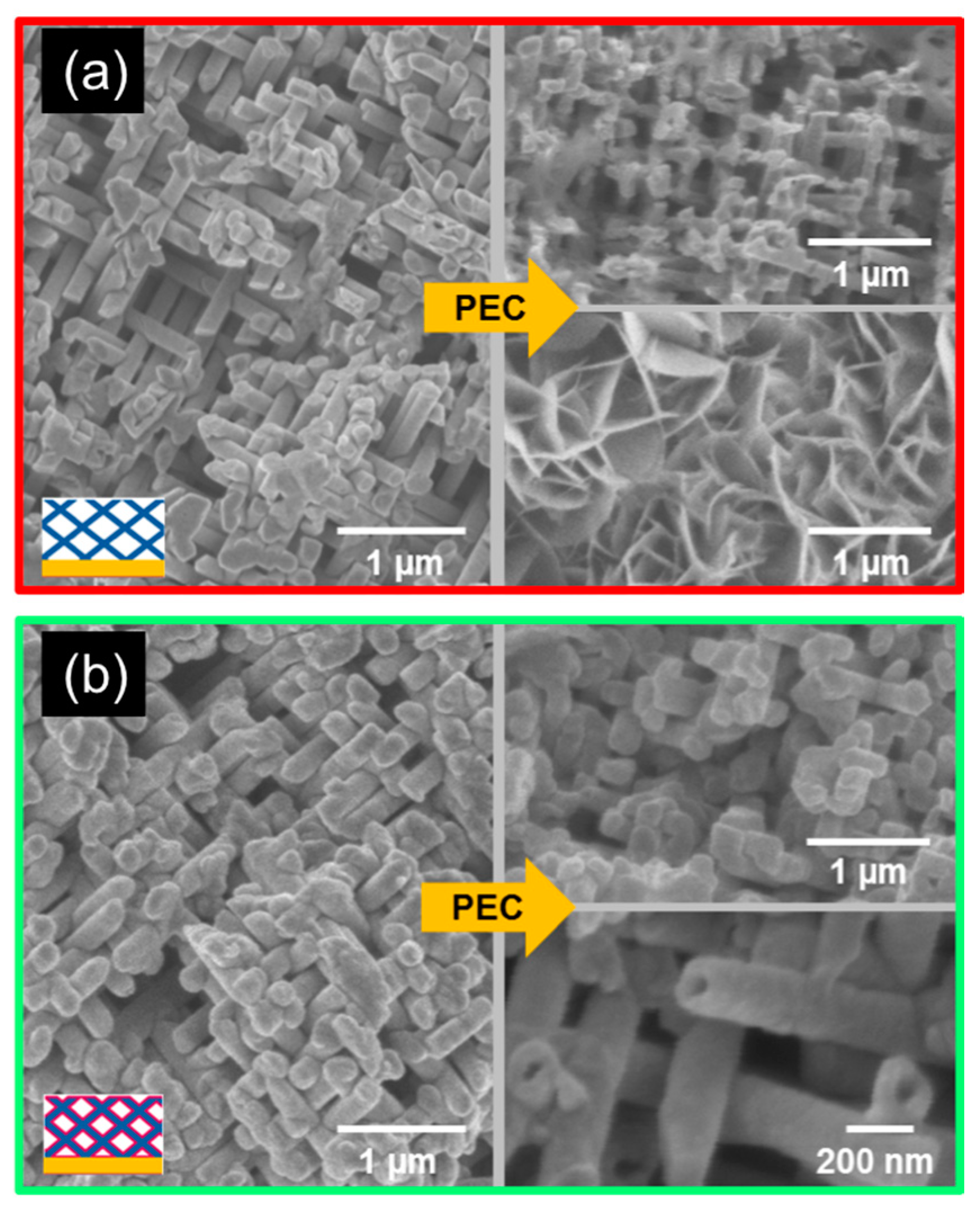
3.2. Photoelectrochemical Measurements
4. Conclusions
Supplementary Materials
Author Contributions
Acknowledgments
Conflicts of Interest
References
- Ponzoni, A.; Comini, E.; Sberveglieri, G.; Zhou, J.; Deng, S.Z.; Xu, N.S.; Ding, Y.; Wang, Z.L. Ultrasensitive and highly selective gas sensors using three-dimensional tungsten oxide nanowire networks. Appl. Phys. Lett. 2006, 88, 20310. [Google Scholar] [CrossRef]
- Alenezi, M.R.; Henley, S.J.; Emerson, N.G.; Silva, S.R.P. From 1D and 2D ZnO nanostructures to 3D hierarchical structures with enhanced gas sensing properties. Nanoscale 2014, 6, 235–247. [Google Scholar] [CrossRef] [PubMed]
- Liu, R.; Duay, J.; Lee, S.B. Heterogeneous nanostructured electrode materials for electrochemical energy storage. Chem. Commun. 2011, 47, 1384–1404. [Google Scholar] [CrossRef] [PubMed]
- Duay, J.; Gillette, E.; Hu, J.; Lee, S.B. Controlled electrochemical deposition and transformation of hetero nanoarchitectured electrodes for energy storage. Phys. Chem. Chem. Phys. 2013, 15, 7976. [Google Scholar] [CrossRef] [PubMed]
- Wei, D.; Scherer, M.R.J.; Bower, C.; Andrew, P.; Ryhänen, T.; Steiner, U. A nanostructured electrochromic supercapacitor. Nano Lett. 2012, 12, 1857–1862. [Google Scholar] [CrossRef] [PubMed]
- Hochbaum, A.I.; Yang, P. Semiconductor nanowires for energy conversion. Chem. Rev. 2010, 110, 527–546. [Google Scholar] [CrossRef] [PubMed]
- Zhong, M.; Ma, Y.; Oleynikov, P.; Domen, K.; Delaunay, J.-J. A conductive ZnO–ZnGaON nanowire-array-on-a-film photoanode for stable and efficient sunlight water splitting. Energy Environ. Sci. 2014, 7, 1693. [Google Scholar] [CrossRef]
- Van de Krol, R.; Liang, Y.; Schoonman, J. Solar hydrogen production with nanostructured metal oxides. J. Mater. Chem. 2008, 18, 2311. [Google Scholar] [CrossRef]
- Liu, M.; Nam, C.-Y.; Black, C.T.; Kamcev, J.; Zhang, L. Enhancing water splitting activity and chemical stability of zinc oxide nanowire photoanodes with ultrathin titania shells. J. Phys. Chem. C 2013, 117, 13396–13402. [Google Scholar] [CrossRef]
- Shi, J.; Hara, Y.; Sun, C.; Anderson, M.A.; Wang, X. 3D High-density hierarchical nanowire architecture for high performance photoelectrochemical electrodes. Nano Lett. 2011, 11, 3413–3419. [Google Scholar] [CrossRef] [PubMed]
- Wang, Y.C.; Tang, J.; Peng, Z.; Wang, Y.H.; Jia, D.S.; Kong, B.; Elzatahry, A.A.; Zhao, D.Y.; Zheng, G.F. Fully solar-powered photoelectrochemical conversion for simultaneous energy storage and chemical sensing. Nano Lett. 2014, 14, 3668–3673. [Google Scholar] [CrossRef] [PubMed]
- Li, Q.; Sun, X.; Lozano, K.; Mao, Y. Facile and scalable synthesis of “Caterpillar-like” ZnO nanostructures with enhanced photoelectrochemical water-splitting effect. J. Phys. Chem. C 2014, 118, 13467–13475. [Google Scholar] [CrossRef]
- Ongaro, M.; Gambirasi, A.; Favarob, M.; Ugo, P. Electrochemical synthesis and characterization of hierarchically branched ZnO nanostructures on ensembles of gold nanowires. Electrochim. Acta 2012, 78, 539–546. [Google Scholar] [CrossRef]
- Elias, J.; Bechelany, M.; Utke, I.; Erni, R.; Hosseini, D.; Michler, J.; Philippe, L. Urchin-inspired zinc oxide as building blocks for nanostructured solar cells. Nano Energy 2012, 1, 696–705. [Google Scholar] [CrossRef]
- Vignolini, S.; Yufa, N.A.; Cunha, P.S.; Guldin, S.; Rushkin, I.; Stefik, M.; Hur, K.; Wiesner, U.; Baumberg, J.J.; Steiner, U. A 3D optical metamaterial made by self-assembly. Adv. Mater. 2012, 24, 23–27. [Google Scholar] [CrossRef] [PubMed]
- Galisteo-López, J.F.; Ibisate, M.; Sapienza, R.; Froufe-Pérez, L.S.; Blanco, Á.; López, C. Self-assembled photonic structures. Adv. Mater. 2011, 23, 30–69. [Google Scholar] [CrossRef] [PubMed]
- Fujishima, A.; Honda, K. Electrochemical photolysis of water at a semiconductor electrode. Nature 1972, 238, 37–38. [Google Scholar] [CrossRef] [PubMed]
- Walter, M.G.; Warren, E.L.; McKone, J.R.; Boettcher, S.W.; Mi, Q.; Santori, E.A.; Lewis, N.S. Solar water splitting cells. Chem. Rev. 2010, 110, 6446–6473. [Google Scholar] [CrossRef] [PubMed]
- Li, Y.; Zhang, J.Z. Hydrogen generation from photoelectrochemical water splitting based on nanomaterials. Laser Photonics Rev. 2010, 4, 517–528. [Google Scholar] [CrossRef]
- Schoonman, J.; Van De Krol, R. Nanostructured materials for solar hydrogen production. U.P.B. Sci. Bull. 2011, 73, 31–44. [Google Scholar] [CrossRef]
- Williams, W.D.; Giordano, N. Fabrication of 80 Å metal wires. Rev. Sci. Instrum. 1984, 55, 410–412. [Google Scholar] [CrossRef]
- Toimil Molares, M.E.; Dobrev, D.; Schuchert, I.U.; Vetter, J.; Neumann, R. Copper nanowires produced by electrochemical deposition in polyneric ion track membranes. Adv. Mater. 2001, 13, 62–65. [Google Scholar] [CrossRef]
- Karim, S.; Toimil-Molares, M.E.; Maurer, F.; Miehe, G.; Ensinger, W.; Liu, J.; Cornelius, T.W.; Neumann, R. Synthesis of gold nanowires with controlled crystallographic characteristics. Appl. Phys. A 2006, 84, 403–407. [Google Scholar] [CrossRef]
- Toimil-Molares, M.E.; Chtanko, N.; Cornelius, T.W.; Dobrev, D.; Enculescu, I.; Blick, R.H.; Neumann, R. Fabrication and contacting of single Bi nanowires. Nanotechnology 2004, 15, 201–207. [Google Scholar] [CrossRef]
- Picht, O.; Müller, S.; Rauber, M.; Lensch-Falk, J.; Medlin, D.L.; Neumann, R.; Sigle, W.; Toimil-Molares, M.E. Tuning the geometrical and crystallographic characteristics of Bi2Te3 nanowires by electrodeposition in ion-track membranes. J. Phys. Chem. C 2012, 116, 5367. [Google Scholar] [CrossRef]
- Rauber, M.; Brötz, J.; Duan, J.; Liu, J.; Müller, S.; Neumann, R.; Picht, O.; Toimil-Molares, M.E.; Ensinger, W. Segmented all-platinum nanowires with controlled morphology through manipulation of the local electrolyte distribution in fluidic nanochannels during electrodeposition. J. Phys. Chem. C 2010, 114, 22502–22507. [Google Scholar] [CrossRef]
- Rauber, M.; Alber, I.; Müller, S.; Neumann, R.; Picht, O.; Roth, C.; Schökel, T.; Toimil-Molares, M.E.; Ensinger, W. Highly-ordered supportless three-dimensional nanowire networks with tunable complexity and interwire connectivity for device integration. Nano Lett. 2011, 11, 2304. [Google Scholar] [CrossRef] [PubMed]
- Manzano, C.V.; Bürki, G.; Pethö, L.; Michler, J.; Philippe, L. Determining the diffusion mechanism for high aspect ratio ZnO nanowires electrodeposited into anodic aluminum oxide. J. Mater. Chem. C 2017, 5, 1706. [Google Scholar] [CrossRef]
- Hulteen, J.C.; Martin, C.R. A general template-based method for the preparation of nanomaterials. J. Mater. Chem. 1997, 7, 1075–1087. [Google Scholar] [CrossRef]
- Pruna, A.; Pullini, D.; Busquets Mataix, D. Influence of deposition potential on structure of ZnO nanowires synthesized in track-etched membranes. J. Electrochem. Soc. 2012, 159, 92–98. [Google Scholar] [CrossRef]
- Maas, M.G.; Rodijk, E.J.B.; Maijenburg, A.W.; Blank, D.H.A. Microstructure development in zinc oxide nanowires and iron oxohydroxide nanotubes by cathodic electrodeposition in nanopores. J. Mater. Res. 2011, 26, 2261–2267. [Google Scholar] [CrossRef]
- Sima, M.; Enculescu, I.; Vasile, E. Growth of ZnO micro and nanowires using the template method. J. Optoelectron. Adv. Mater. 2006, 8, 825. [Google Scholar]
- Ongaro, M.; Mardegan, A.; Stortini, A.M.; Signoretto, M.; Ugo, P. Arrays of templated TiO2 nanofibres as improved photoanodes for water splitting under visible light. Nanotechnology 2015, 26, 165402. [Google Scholar] [CrossRef] [PubMed]
- Ferain, E.; Legras, R. Heavy ion tracks in polycarbonate. Comparison with a heavy ion irradiated model compound. Nucl. Instrum. Methods Phys. Res. Sect. B 1993, 82, 539–548. [Google Scholar] [CrossRef]
- Movsesyan, L.; Schubert, I.; Yeranyan, L.; Trautmann, C.; Toimil-Molares, M.E. Influence of electrodeposition parameters on the structure and morphology of ZnO nanowire arrays and networks synthesized in etched ion-track membranes. Semicond. Sci. Technol. 2015, 31, 014006. [Google Scholar] [CrossRef]
- Toimil-Molares, M.E. Characterization and properties of micro- and nanowires of controlled size, composition, and geometry fabricated by electrodeposition and ion-track technology. Beilstein J. Nanotechnol. 2012, 3, 860–883. [Google Scholar] [CrossRef] [PubMed]
- Movsesyan, L. Template-Assisted Growth and Characterization of ZnO Based Nanowire Arrays and 3D Networks. Ph.D. Thesis, Technische Universität Darmstadt, Darmstadt, Germany, 2016. [Google Scholar]
- Hu, S.; Shaner, M.R.; Beardslee, J.A.; Lichterman, M.; Brunschwig, B.S.; Lewis, N.S. Amorphous TiO2 coatings stabilize Si, GaAs, and GaP photoanodes for efficient water oxidation. Science 2014, 344, 1005. [Google Scholar] [CrossRef] [PubMed]
- Wu, L.; Tsui, L.-K.; Swami, N.; Zangari, G. Photoelectrochemical stability of electrodeposited Cu2O films. J. Phys. Chem. C 2010, 114, 11551–11556. [Google Scholar] [CrossRef]
- Gerischer, H. On the stability of semiconductor electrodes against photodecomposition. J. Electroanal. Chem. Interfacial Electrochem. 1977, 82, 133. [Google Scholar] [CrossRef]
- Pourbaix, M. Atlas of Electrochemical Equilibria in Aqueous Solutions, 1st ed.; Pergamon Press: Oxford, UK, 1966. [Google Scholar]
- Liu, C.-F.; Lu, Y.-J.; Hu, C.-C. Effects of anions and pH on the stability of ZnO nanorods for photoelectrochemical water splitting. ACS Omega 2018, 3, 3429–3439. [Google Scholar] [CrossRef]


© 2018 by the authors. Licensee MDPI, Basel, Switzerland. This article is an open access article distributed under the terms and conditions of the Creative Commons Attribution (CC BY) license (http://creativecommons.org/licenses/by/4.0/).
Share and Cite
Movsesyan, L.; Maijenburg, A.W.; Goethals, N.; Sigle, W.; Spende, A.; Yang, F.; Kaiser, B.; Jaegermann, W.; Park, S.-Y.; Mul, G.; et al. ZnO Nanowire Networks as Photoanode Model Systems for Photoelectrochemical Applications. Nanomaterials 2018, 8, 693. https://doi.org/10.3390/nano8090693
Movsesyan L, Maijenburg AW, Goethals N, Sigle W, Spende A, Yang F, Kaiser B, Jaegermann W, Park S-Y, Mul G, et al. ZnO Nanowire Networks as Photoanode Model Systems for Photoelectrochemical Applications. Nanomaterials. 2018; 8(9):693. https://doi.org/10.3390/nano8090693
Chicago/Turabian StyleMovsesyan, Liana, Albert Wouter Maijenburg, Noel Goethals, Wilfried Sigle, Anne Spende, Florent Yang, Bernhard Kaiser, Wolfram Jaegermann, Sun-Young Park, Guido Mul, and et al. 2018. "ZnO Nanowire Networks as Photoanode Model Systems for Photoelectrochemical Applications" Nanomaterials 8, no. 9: 693. https://doi.org/10.3390/nano8090693
APA StyleMovsesyan, L., Maijenburg, A. W., Goethals, N., Sigle, W., Spende, A., Yang, F., Kaiser, B., Jaegermann, W., Park, S.-Y., Mul, G., Trautmann, C., & Toimil-Molares, M. E. (2018). ZnO Nanowire Networks as Photoanode Model Systems for Photoelectrochemical Applications. Nanomaterials, 8(9), 693. https://doi.org/10.3390/nano8090693