Fabrication of Scaffold-Based 3D Magnetic Nanowires for Domain Wall Applications

 ,
,  ,
,  , ,
, , 
Abstract
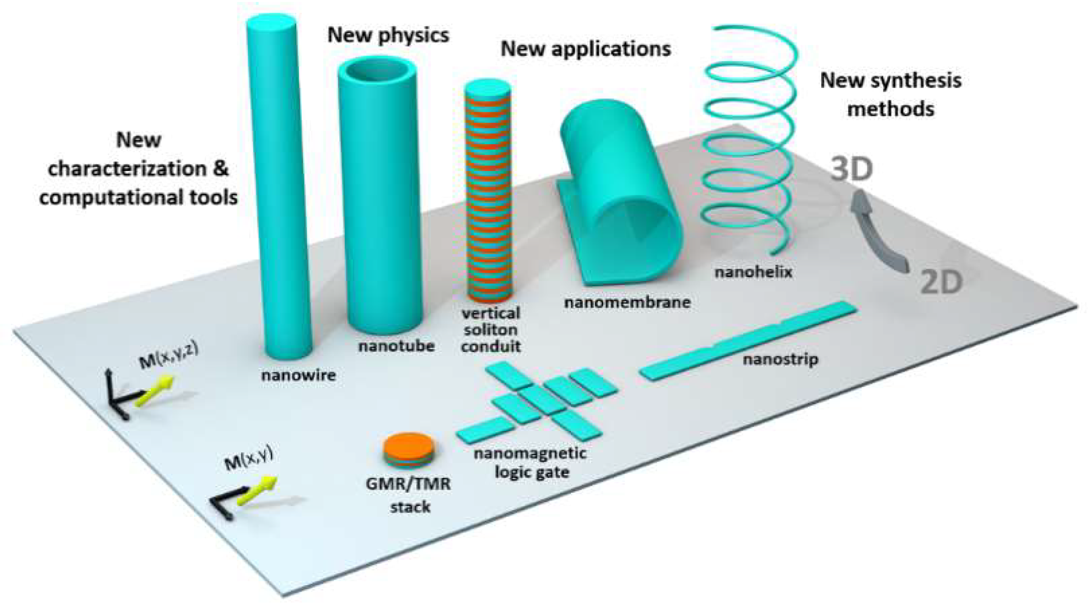
1. Introduction
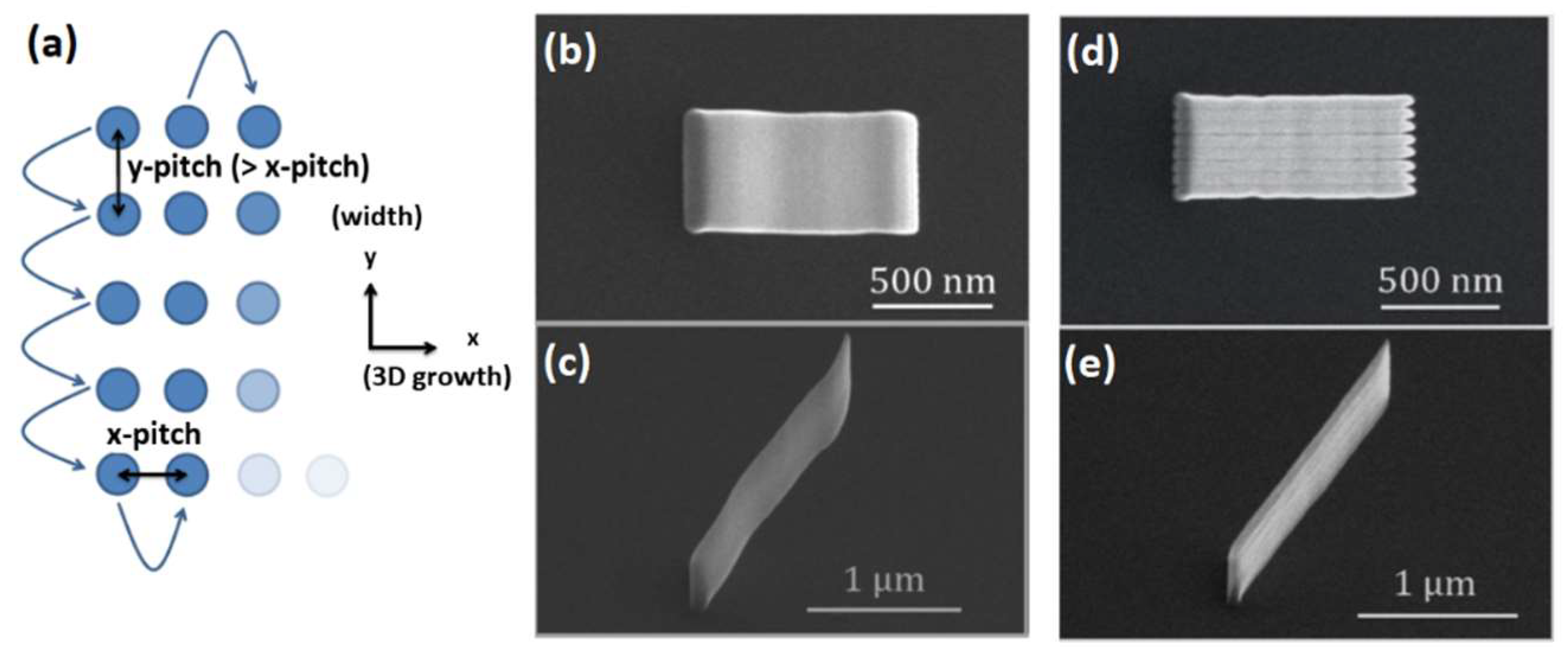
- Nanostructure width (segments become flat nanowires) is achieved by using a dual-pitch pattering strategy.
- The catalogue of accessible materials is expanded by combining 3D nano-printing with physical deposition methods.
- Growth limitations for low segment-angle structures are overcome by employing substrate tilting during growth.
2. Materials and Methods
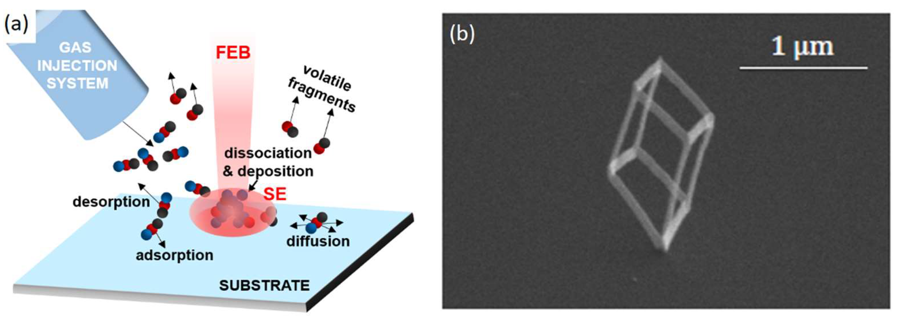
2.1. 3D-Nanoprinting by Focused Electron Beam Induced Deposition (FEBID)
2.2. FEBID Parameters and Calibration
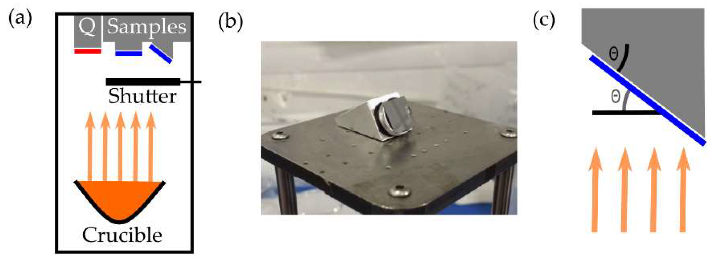
2.3. Thermal Evaporation of Magnetic Material
3. Results
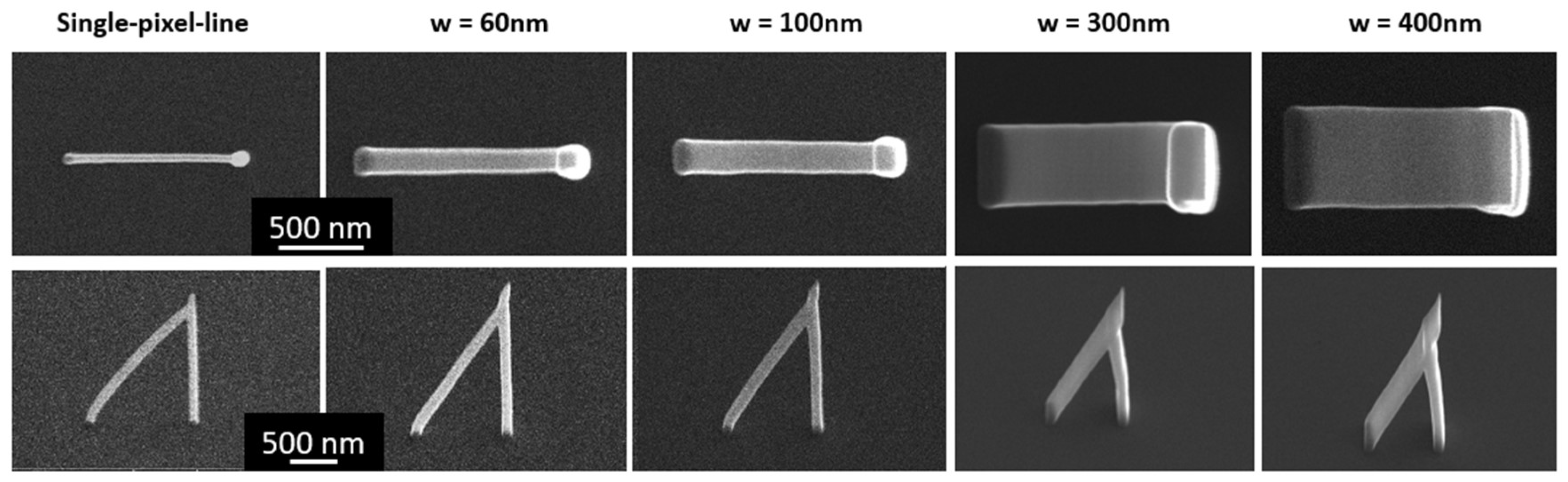
3.1. Wide Nanostructures: Dual-Pitch Nanopatterning
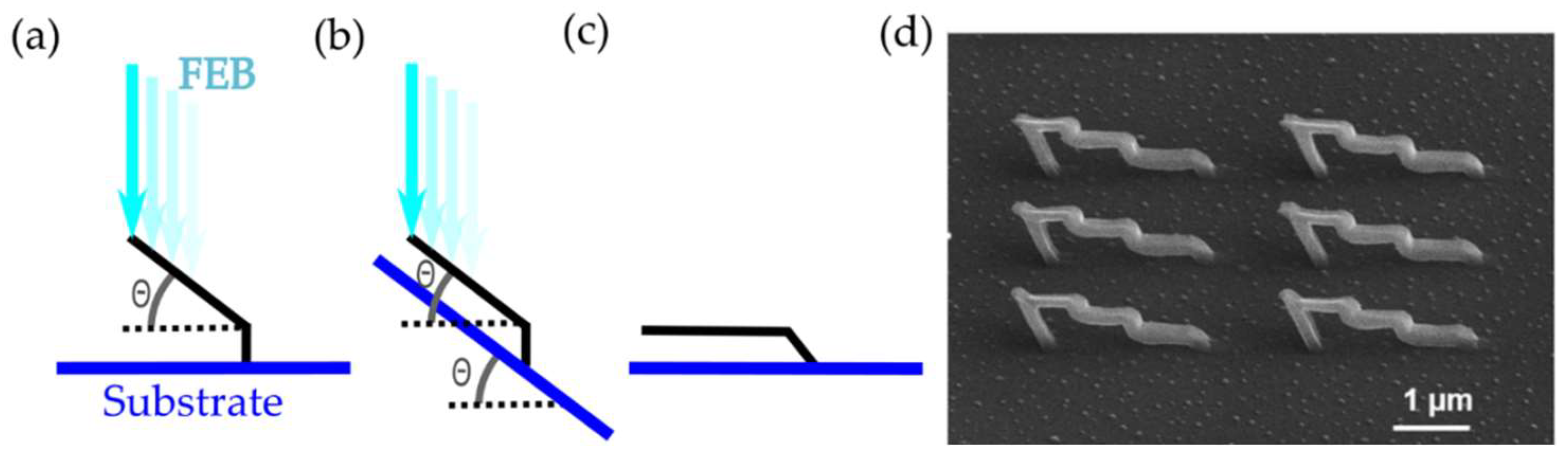
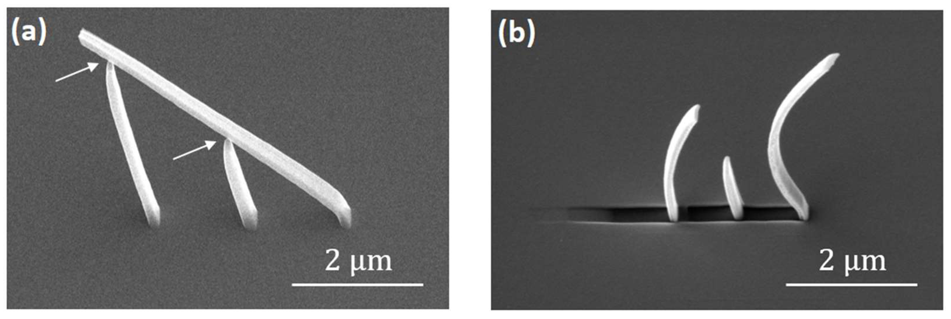
3.2. Horizontal Nanoprinting Using Substrate Tilt
3.3. Thin-Film Evaporation onto 3d Scaffolds
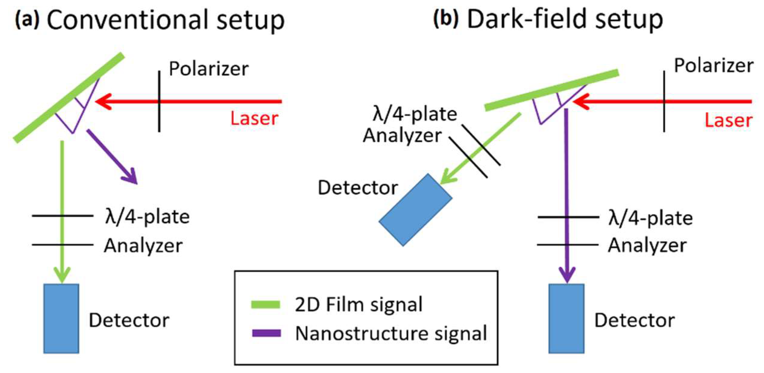
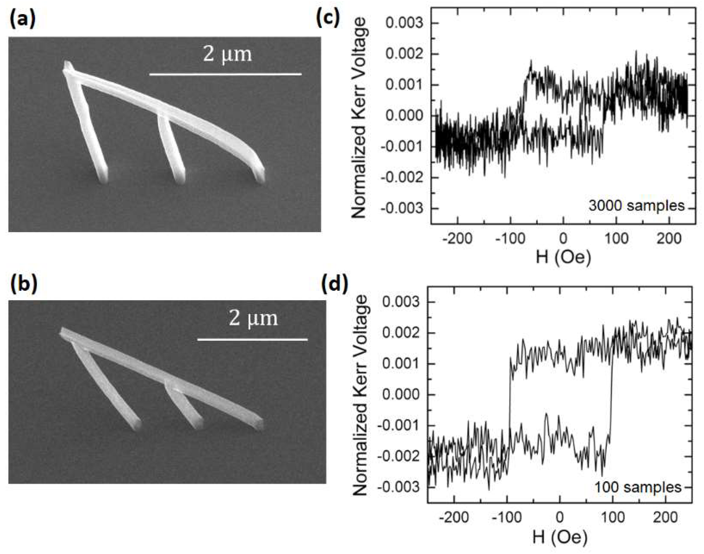
3.4. Tailored Design for Magneto-Optical Detection
4. Discussion
Notice of Copyright
Author Contributions
Funding
Metadata
Acknowledgments
Conflicts of Interest
References
- Sander, D.; Valenzuela, S.O.; Makarov, D.; Marrows, C.H.; Fullerton, E.E.; Fischer, P.; McCord, J.; Vavassori, P.; Mangin, S.; Pirro, P.; et al. The 2017 Magnetism Roadmap. J. Phys. D. Appl. Phys. 2017, 50, 363001. [Google Scholar] [CrossRef]
- Fernández-Pacheco, A.; Streubel, R.; Fruchart, O.; Hertel, R.; Fischer, P.; Cowburn, R.P. Three-dimensional nanomagnetism. Nat. Commun. 2017, 8, 15756. [Google Scholar] [CrossRef] [PubMed]
- Schmidt, O.G.; Eberl, K. Thin solid films roll up into nanotubes. Nature 2001, 410, 168. [Google Scholar] [CrossRef] [PubMed]
- Sousa, C.T.; Leitao, D.C.; Proenca, M.P.; Ventura, J.; Pereira, A.M.; Araujo, J.P. Nanoporous alumina as templates for multifunctional applications. Appl. Phys. Rev. 2014, 1, 031102. [Google Scholar] [CrossRef]
- Albrecht, M.; Hu, G.; Guhr, I.L.; Ulbrich, T.C.; Boneberg, J.; Leiderer, P.; Schatz, G. Magnetic multilayers on nanospheres. Nat. Mater. 2005, 4, 203–206. [Google Scholar] [CrossRef] [PubMed]
- Donnelly, C.; Guizar-Sicairos, M.; Scagnoli, V.; Holler, M.; Huthwelker, T.; Menzel, A.; Vartiainen, I.; Müller, E.; Kirk, E.; Gliga, S.; et al. Element-specific X-Ray phase tomography of 3D structures at the nanoscale. Phys. Rev. Lett. 2015, 114, 115501. [Google Scholar] [CrossRef] [PubMed]
- Tottori, S.; Zhang, L.; Qiu, F.; Krawczyk, K.K.; Franco-Obregón, A.; Nelson, B.J. Magnetic Helical Micromachines: Fabrication, Controlled Swimming, and Cargo Transport. Adv. Mater. 2012, 24, 811–816. [Google Scholar] [CrossRef] [PubMed]
- De Teresa, J.M.; Fernández-Pacheco, A.; Córdoba, R.; Serrano-Ramón, L.; Sangiao, S.; Ibarra, M.R. Review of magnetic nanostructures grown by focused electron beam induced deposition (FEBID). J. Phys. D. Appl. Phys. 2016, 49, 243003. [Google Scholar] [CrossRef]
- Sanz-Hernández, D.; Fernández-Pacheco, A. Modelling focused electron beam induced deposition beyond Langmuir adsorption. Beilstein J. Nanotechnol. 2017, 8, 2151–2161. [Google Scholar] [CrossRef] [PubMed]
- Fowlkes, J.D.; Winkler, R.; Lewis, B.B.; Fernández-Pacheco, A.; Skoric, L.; Sanz-Hernández, D.; Stanford, M.G.; Mutunga, E.; Rack, P.D.; Plank, H. High-Fidelity 3D-Nanoprinting via Focused Electron Beams: Computer-Aided Design (3BID). ACS Appl. Nano Mater. 2018, 1, 1028–1041. [Google Scholar] [CrossRef]
- Sanz-Hernández, D.; Hamans, R.F.; Liao, J.W.; Welbourne, A.; Lavrijsen, R.; Fernández-Pacheco, A. Fabrication, Detection, and Operation of a Three-Dimensional Nanomagnetic Conduit. ACS Nano 2017, 11, 11066–11073. [Google Scholar] [CrossRef] [PubMed]
- Utke, I.; Hoffmann, P.; Melngailis, J. Gas-assisted focused electron beam and ion beam processing and fabrication. J. Vac. Sci. Technol. B 2008, 26, 1197. [Google Scholar] [CrossRef]
- Van Dorp, W.F.; Hagen, C.W. A critical literature review of focused electron beam induced deposition. J. Appl. Phys. 2008, 104, 081301. [Google Scholar] [CrossRef]
- Winkler, R.; Lewis, B.B.; Fowlkes, J.D.; Rack, P.D.; Plank, H. High-Fidelity 3D-Nanoprinting via Focused Electron Beams: Growth Fundamentals. ACS Appl. Nano Mater. 2018, 1, 1014–1027. [Google Scholar] [CrossRef]
- Fowlkes, J.D.; Winkler, R.; Lewis, B.B.; Stanford, M.G.; Plank, H.; Rack, P.D. Simulation-Guided 3D Nanomanufacturing via Focused Electron Beam Induced Deposition. ACS Nano 2016, 10, 6163–6172. [Google Scholar] [CrossRef] [PubMed]
- Drouin, D.; Couture, A.R.; Joly, D.; Tastet, X.; Aimez, V.; Gauvin, R. CASINO V2.42: A Fast and Easy to use Modeling Tool for Scanning Electron Microscopy and Microanalysis Users. Scanning 2007, 29, 92–101. [Google Scholar] [CrossRef] [PubMed]
- Mukherjee, D.; Hordagoda, M.; Hyde, R.; Bingham, N.; Srikanth, H.; Witanachchi, S.; Mukherjee, P. Nanocolumnar Interfaces and Enhanced Magnetic Coercivity in Preferentially oriented Cobalt Ferrite Thin Films Grown Using Oblique-Angle Pulsed Laser Deposition. ACS Appl. Mater. Interfaces 2013, 5, 7450–7457. [Google Scholar] [CrossRef] [PubMed]
- Keller, L.; Al Mamoori, M.K.I.; Pieper, J.; Gspan, C.; Stockem, I.; Schröder, C.; Barth, S.; Winkler, R.; Plank, H.; Pohlit, M.; et al. Direct-write of free-form building blocks for artificial magnetic 3D lattices. Sci. Rep. 2018, 8, 6160. [Google Scholar] [CrossRef] [PubMed]
- Pauleau, Y. Generation and evolution of residual stresses in physical vapour-deposited thin films. Vacuum 2001, 61, 175–181. [Google Scholar] [CrossRef]
- Fernández-Pacheco, A.; Serrano-Ramón, L.; Michalik, J.M.; Ibarra, M.R.; De Teresa, J.M.; O’Brien, L.; Petit, D.; Lee, J.; Cowburn, R.P. Three dimensional magnetic nanowires grown by focused electron-beam induced deposition. Sci. Rep. 2013, 3, 1492. [Google Scholar] [CrossRef] [PubMed]
- Verduci, T.; Rufo, C.; Berger, A.; Metlushko, V.; Ilic, B.; Vavassori, P. Fourier magnetic imaging. Appl. Phys. Lett. 2011, 99, 092501. [Google Scholar] [CrossRef]
- Westphalen, A.; Lee, M.-S.; Remhof, A.; Zabel, H. Invited article: Vector and Bragg Magneto-optical Kerr effect for the analysis of nanostructured magnetic arrays. Rev. Sci. Instrum. 2007, 78, 121301. [Google Scholar] [CrossRef] [PubMed]
- Allwood, D.A.; Vernier, N.; Xiong, G.; Cooke, M.D.; Atkinson, D.; Faulkner, C.C.; Cowburn, R.P. Shifted hysteresis loops from magnetic nanowires. Appl. Phys. Lett. 2002, 81, 4005–4007. [Google Scholar] [CrossRef]


© 2018 by the authors. Licensee MDPI, Basel, Switzerland. This article is an open access article distributed under the terms and conditions of the Creative Commons Attribution (CC BY) license (http://creativecommons.org/licenses/by/4.0/).
Share and Cite
Sanz-Hernández, D.; Hamans, R.F.; Osterrieth, J.; Liao, J.-W.; Skoric, L.; Fowlkes, J.D.; Rack, P.D.; Lippert, A.; Lee, S.F.; Lavrijsen, R.; et al. Fabrication of Scaffold-Based 3D Magnetic Nanowires for Domain Wall Applications. Nanomaterials 2018, 8, 483. https://doi.org/10.3390/nano8070483
Sanz-Hernández D, Hamans RF, Osterrieth J, Liao J-W, Skoric L, Fowlkes JD, Rack PD, Lippert A, Lee SF, Lavrijsen R, et al. Fabrication of Scaffold-Based 3D Magnetic Nanowires for Domain Wall Applications. Nanomaterials. 2018; 8(7):483. https://doi.org/10.3390/nano8070483
Chicago/Turabian StyleSanz-Hernández, Dédalo, Ruben F. Hamans, Johannes Osterrieth, Jung-Wei Liao, Luka Skoric, Jason D. Fowlkes, Philip D. Rack, Anna Lippert, Steven F. Lee, Reinoud Lavrijsen, and et al. 2018. "Fabrication of Scaffold-Based 3D Magnetic Nanowires for Domain Wall Applications" Nanomaterials 8, no. 7: 483. https://doi.org/10.3390/nano8070483
APA StyleSanz-Hernández, D., Hamans, R. F., Osterrieth, J., Liao, J.-W., Skoric, L., Fowlkes, J. D., Rack, P. D., Lippert, A., Lee, S. F., Lavrijsen, R., & Fernández-Pacheco, A. (2018). Fabrication of Scaffold-Based 3D Magnetic Nanowires for Domain Wall Applications. Nanomaterials, 8(7), 483. https://doi.org/10.3390/nano8070483