An InGaN/GaN Superlattice to Enhance the Performance of Green LEDs: Exploring the Role of V-Pits

 ,
, 
Abstract
1. Introduction
2. Materials and Methods
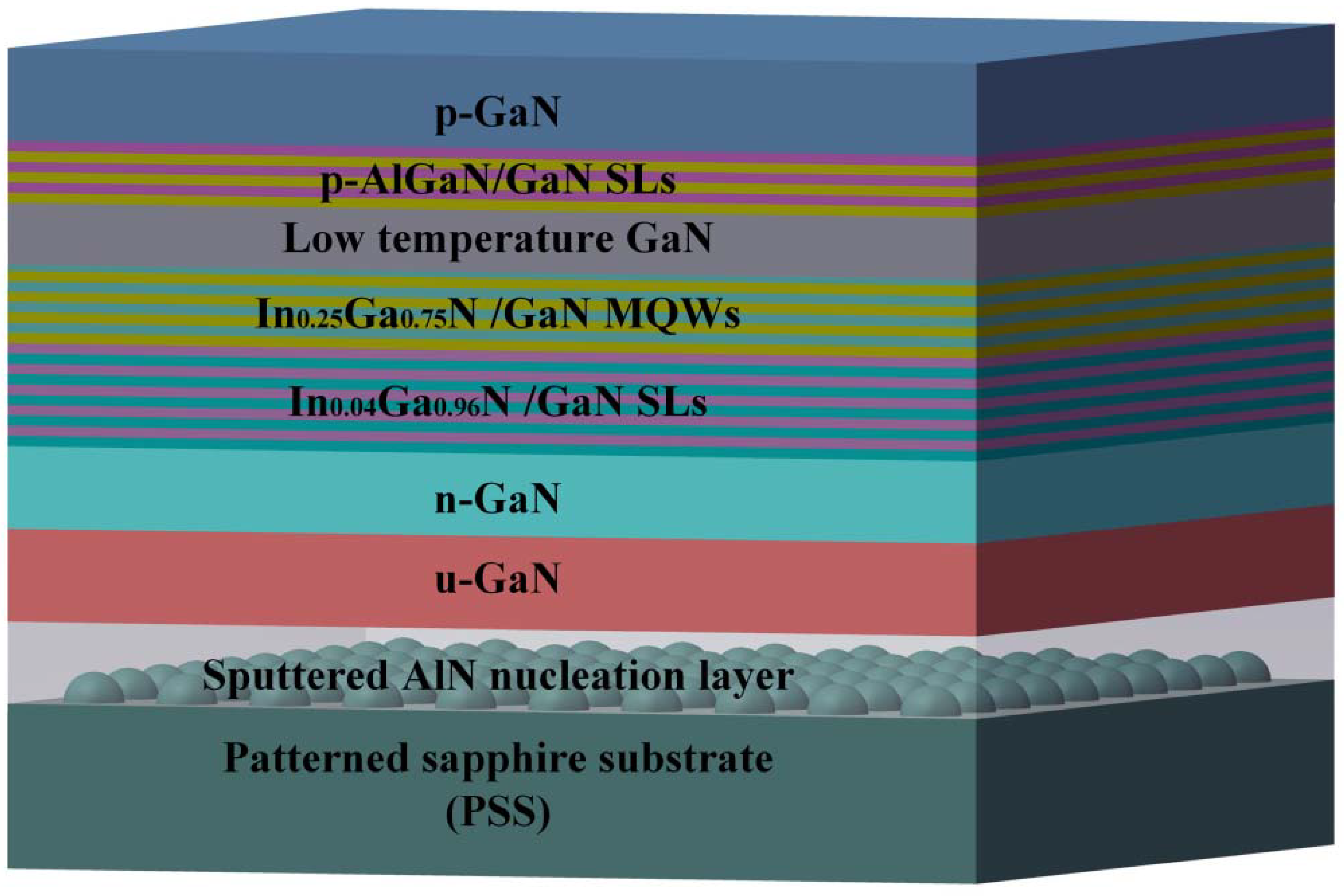
2.1. Growth and Device Fabrication
2.2. Material Characterization and Measurement
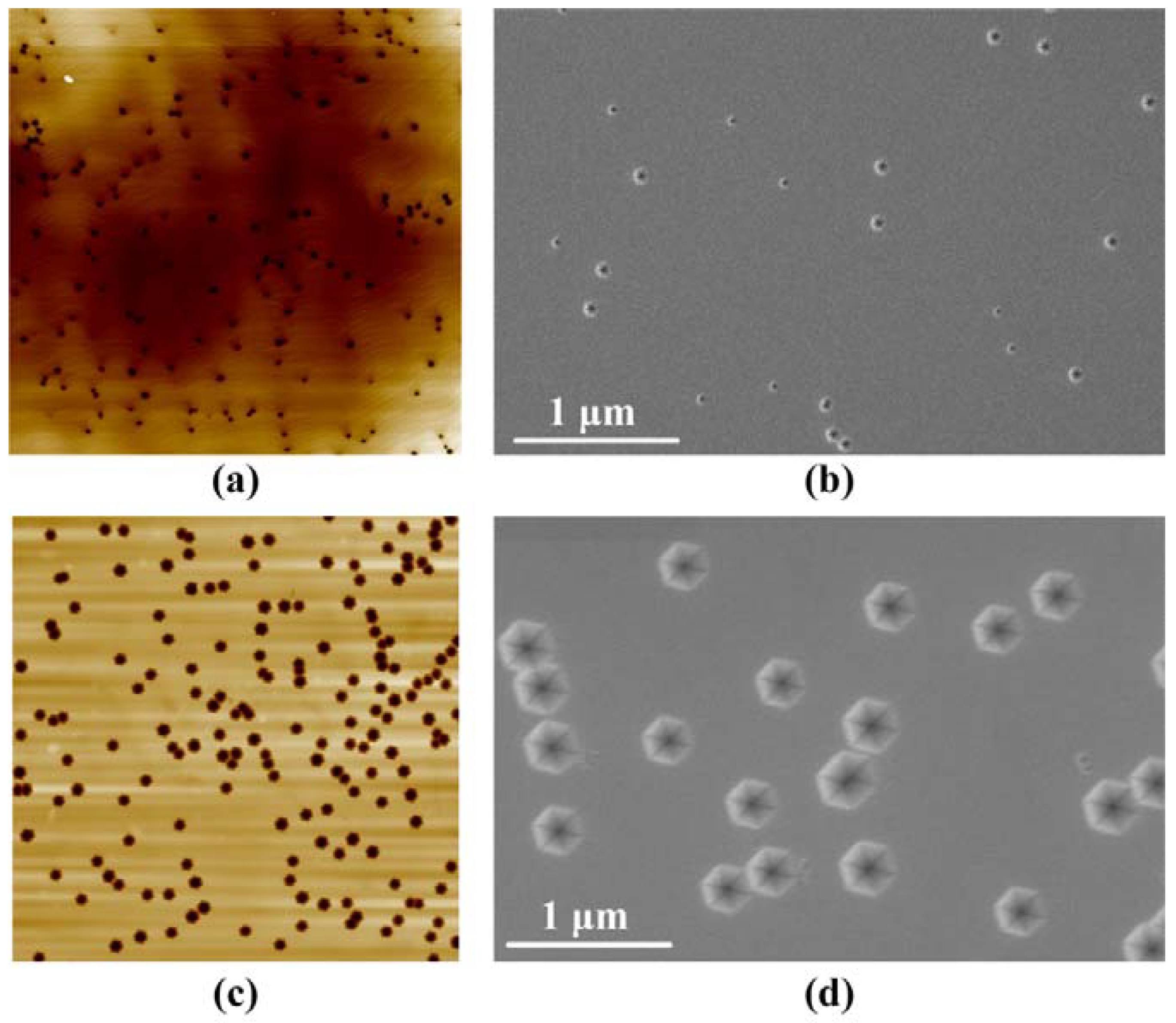
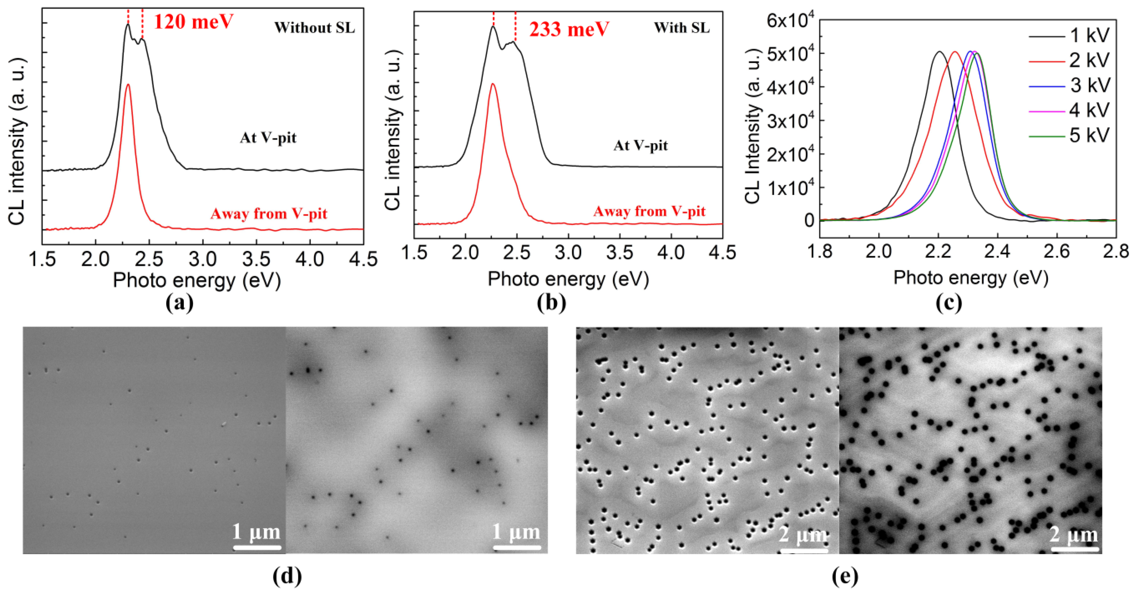
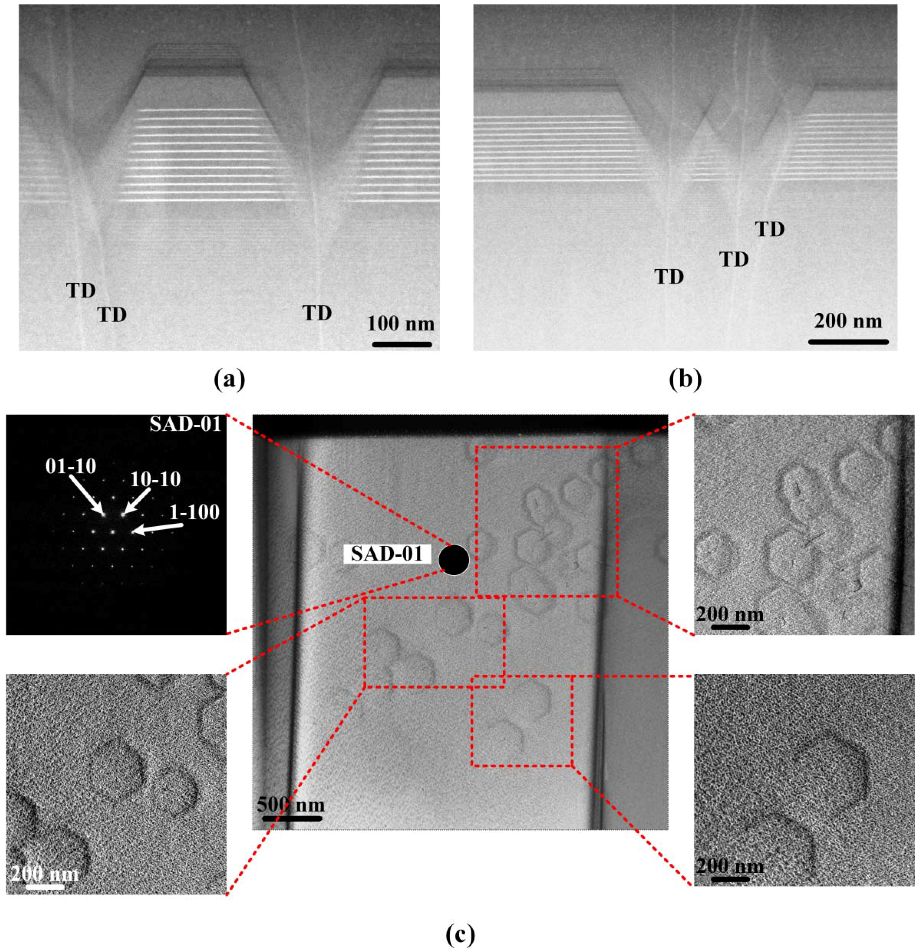
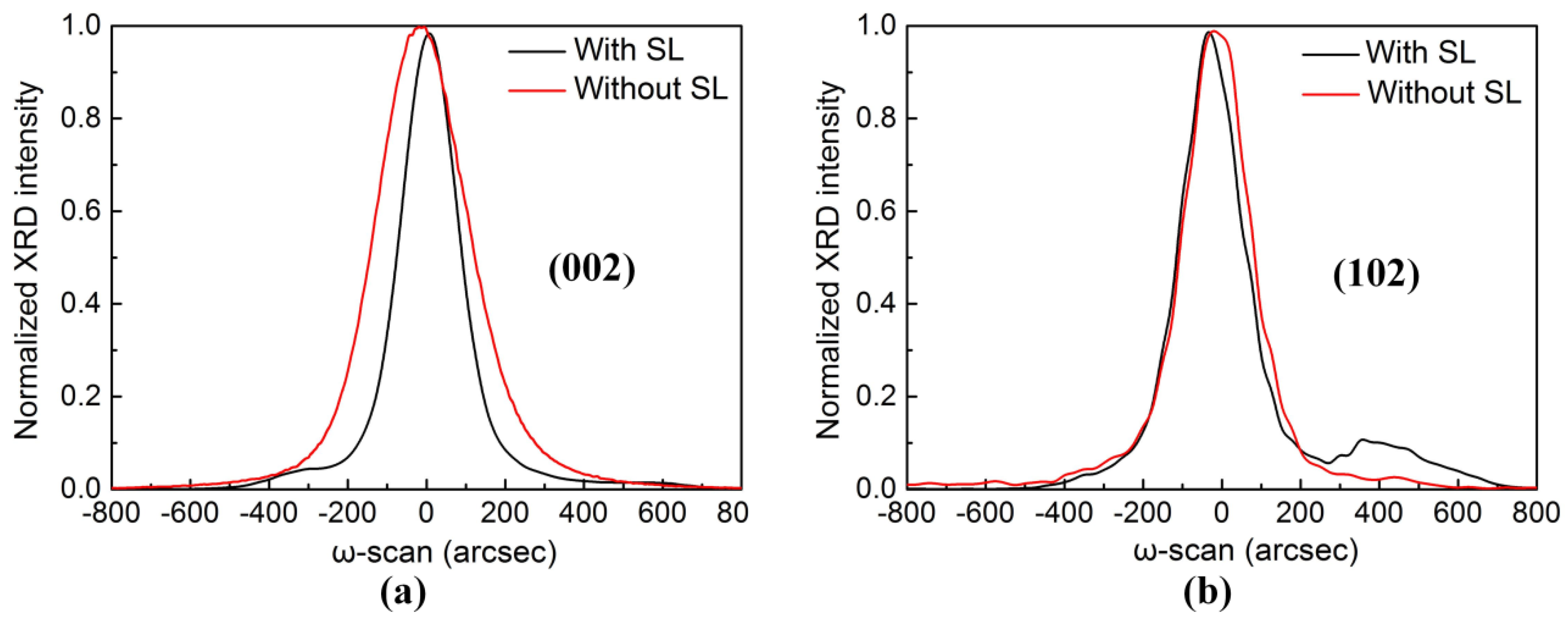
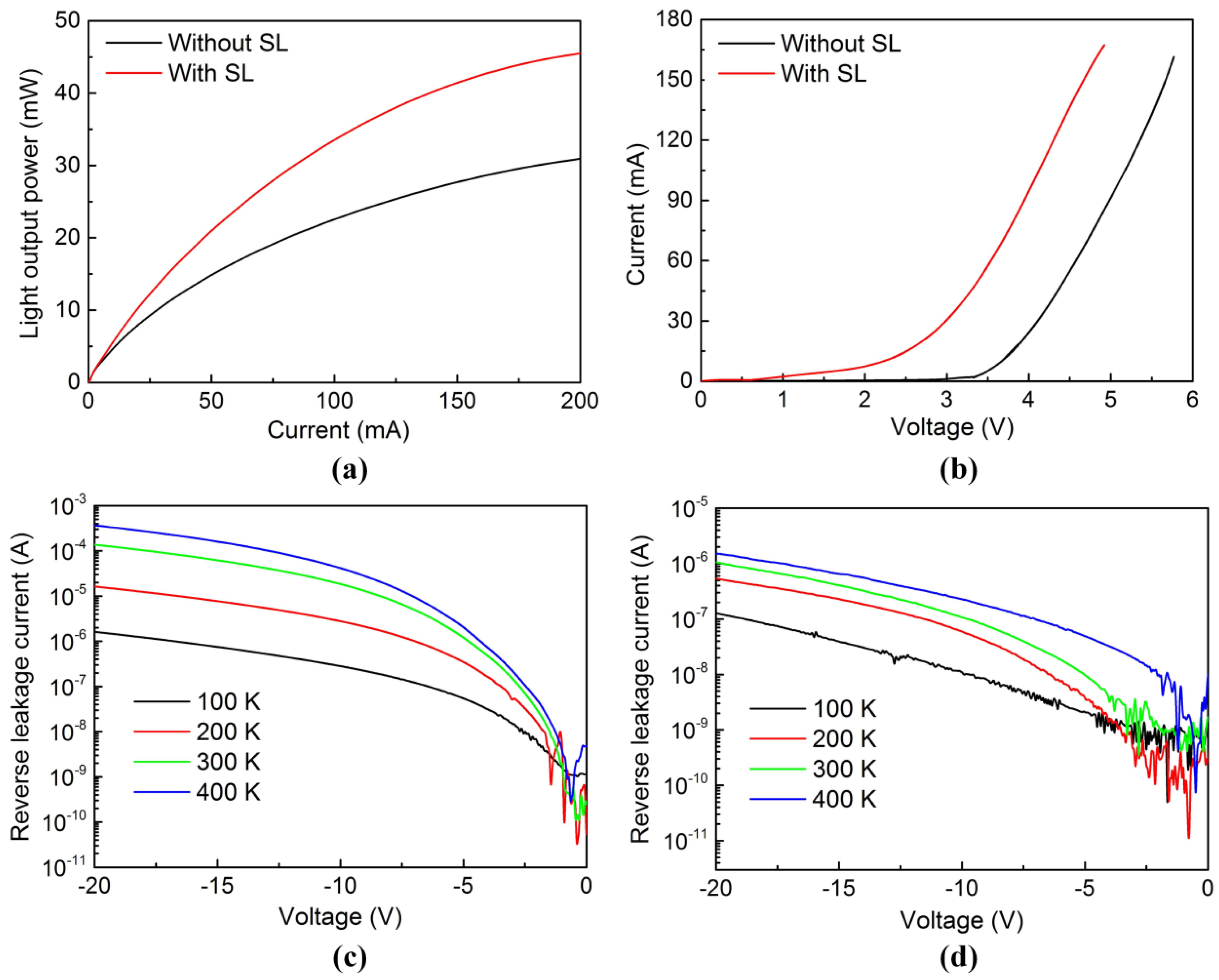
3. Results and Discussion
4. Conclusions
Author Contributions
Funding
Conflicts of Interest
References
- Mukai, T.; Yamada, M.; Nakamura, S. Characteristics of InGaN-based UV/blue/green/amber/red light-emitting diodes. Jpn. J. Appl. Phys. 1999, 38, 3976–3981. [Google Scholar] [CrossRef]
- Takano, T.; Mino, T.; Sakai, J.; Noguchi, N.; Tsubaki, K.; Hirayama, H. Deep-ultraviolet light-emitting diodes with external quantum efficiency higher than 20% at 275 nm achieved by improving light-extraction efficiency. Appl. Phys. Express 2017, 10, 031002. [Google Scholar] [CrossRef]
- Zhou, S.; Liu, S. Study on sapphire removal for thin-film LEDs fabrication using CMP and dry etching. Appl. Surf. Sci. 2009, 255, 9469–9473. [Google Scholar] [CrossRef]
- Massabuau, F.C.; Chen, P.; Horton, M.K.; Rhode, S.L.; Ren, C.X.; O’Hanlon, T.J.; Kovacs, A.; Kappers, M.J.; Humphreys, C.J.; Dunin-Borkowski, R.E.; et al. Carrier localization in the vicinity of dislocations in InGaN. J. Appl. Phys. 2017, 121, 013104. [Google Scholar] [CrossRef]
- Zhou, S.; Liu, X.; Gao, Y.; Liu, Y.; Liu, M.; Liu, Z.; Gui, C.; Liu, S. Numerical and experimental investigation of GaN-based flip-chip light-emitting diodes with highly reflective Ag/TiW and ITO/DBR Ohmic contacts. Opt. Express 2017, 25, 26615–26627. [Google Scholar] [CrossRef] [PubMed]
- Feng, Y.; Chen, Z.; Jiang, S.; Li, C.; Chen, Y.; Zhan, J.; Chen, Y.; Nie, J.; Jiao, F.; Kang, X.; et al. Study on the coupling mechanism of the orthogonal dipoles with surface plasmon in green LED by cathodoluminescence. Nanomaterials 2018, 8, 244. [Google Scholar] [CrossRef] [PubMed]
- Hu, H.; Zhou, S.; Liu, X.; Gao, Y.; Gui, C.; Liu, S. Effects of GaN/AlGaN/Sputtered AlN nucleation layers on performance of GaN-based ultraviolet light-emitting diodes. Sci. Rep. 2017, 7, 44627. [Google Scholar] [CrossRef] [PubMed]
- Maur, M.A.; Pecchi, A.; Penazzi, G.; Rodrigues, W.; Carlo, A.D. Efficiency drop in green InGaN/GaN light emitting diodes: The role of random alloy fluctuations. Phys. Rev. Lett. 2016, 116, 027401. [Google Scholar] [CrossRef] [PubMed]
- Liu, J.; Jia, Z.; Ma, S.; Dong, H.; Zhai, G.; Xu, B. Enhancement of carrier localization effect and internal quantum efficiency through In-rich InGaN quantum dots. Superlattice Microstruct. 2018, 113, 497–501. [Google Scholar] [CrossRef]
- Karpov, S.Y. Carrier localization in InGaN by composition fluctuations: Implication to the “green gap”. Photonics Res. 2017, 5, A7–A12. [Google Scholar] [CrossRef]
- Sano, T.; Doi, T.; Inada, S.A.; Sugiyama, T.; Honda, Y.; Amano, H.; Yoshino, T. High internal quantum efficiency blue-green light-emitting diode with small efficiency droop fabricated on low dislocation density GaN substrate. Jpn. J. Appl. Phys. 2013, 52, 08JK09. [Google Scholar] [CrossRef]
- Liu, L.; Ling, M.; Yang, J.; Xiong, W.; Jia, W.; Wang, G. Efficiency degradation behaviors of current/thermal co-stressed GaN-based blue light emitting diodes with vertical-structure. J. Appl. Phys. 2012, 111, 093110. [Google Scholar] [CrossRef]
- Zhou, S.; Yuan, S.; Liu, Y.; Guo, L.J.; Liu, S.; Ding, H. Highly efficient and reliable high power LEDs with patterned sapphire substrate and strip-shaped distributed current blocking layer. Appl. Surf. Sci. 2015, 355, 1013–1019. [Google Scholar] [CrossRef]
- Chang, C.Y.; Li, H.; Shih, Y.T.; Lu, T.C. Manipulation of nanoscale V-pits to optimize internal quantum efficiency of InGaN multiple quantum wells. Appl. Phys. Lett. 2015, 106, 091104. [Google Scholar] [CrossRef]
- Takeuchi, T.; Wetzel, C.; Yamaguchi, S.; Sakai, H.; Amano, H.; Akasaki, I. Determination of piezoelectric fields in strained GaInN quantum wells using the quantum-confined Stark effect. Appl. Phys. Lett. 1998, 73, 1691–1693. [Google Scholar] [CrossRef]
- Leem, S.J.; Shin, Y.C.; Kim, K.C.; Kim, E.H.; Sung, Y.M.; Moon, Y.; Hwang, S.M.; Kim, T.G. The effect of the low-mole InGaN structure and InGaN/GaN strained layer superlattices on optical performance of multiple quantum well active layers. J. Cryst. Growth 2008, 311, 103–106. [Google Scholar] [CrossRef]
- Jeong, H.; Jeong, H.J.; Oh, H.M.; Hong, C.H.; Suh, E.K.; Lerondel, G.; Jeong, M.S. Carrier localization in In-rich InGaN/GaN multiple quantum wells for green light-emitting diodes. Sci. Rep. 2015, 5, 9373. [Google Scholar] [CrossRef] [PubMed]
- Chang, S.P.; Wang, C.H.; Chiu, C.H.; Li, J.C.; Lu, Y.S.; Li, Z.Y.; Yang, H.C.; Kuo, H.C.; Lu, T.C.; Wang, S.C. Characteristics of efficiency droop in GaN-based light emitting diodes with an insertion layer between the multiple quantum wells and GaN layer. Appl. Phys. Lett. 2010, 97, 251114. [Google Scholar] [CrossRef]
- Tsai, Y.L.; Liu, C.Y.; Krishnan, C.; Lin, D.W.; Chu, Y.C.; Chen, T.P.; Shen, T.L.; Kao, T.S.; Charlton, M.D.B.; Yu, P.; et al. Bridging the “green gap” of LEDs: Giant light output enhancement and directional control of LEDs via embedded nano-void photonic crystals. Nanoscale 2016, 8, 1192–1199. [Google Scholar] [CrossRef] [PubMed]
- Tomiya, S.; Kanitani, Y.; Tanaka, S.; Ohkubo, T.; Hono, K. Atomic scale characterization of GaInN/GaN multiple quantum wells in V-shaped pits. Appl. Phys. Lett. 2011, 98, 181904. [Google Scholar] [CrossRef]
- Cho, H.K.; Lee, J.Y.; Yang, G.M.; Kim, C.S. Formation mechanism of V defects in the InGaN/GaN multiple quantum wells grown on GaN layers with low threading dislocation density. Appl. Phys. Lett. 2001, 79, 215–217. [Google Scholar] [CrossRef]
- Wu, X.H.; Elsass, C.R.; Abare, A.; Mack, M.; Keller, S.; Petroff, P.M.; DenBaars, S.P.; Rosner, S.J. Structural origin of V-defects and correlation with localized excitonic centers in InGaN/GaN multiple quantum wells. Appl. Phys. Lett. 1998, 72, 692–694. [Google Scholar] [CrossRef]
- Shiojiri, M.; Chuo, C.C.; Hsu, J.T.; Yang, J.R.; Saijo, H. Structure and formation mechanism of V defects in multiple InGaN/GaN quantum well layers. J. Appl. Phys. 2006, 99, 073505. [Google Scholar] [CrossRef]
- Kim, J.; Kim, J.; Tak, Y.; Chae, S.; Kim, J.Y.; Park, Y. Effect of V-shaped pit size on the reverse leakage current of InGaN/GaN light-emitting diodes. IEEE Electron Device Lett. 2013, 34, 1409–1411. [Google Scholar] [CrossRef]
- Hangleiter, A.; Hitzel, F.; Netzel, C.; Fuhrmann, D.; Rossow, U.; Ade, G.; Hinze, P. Suppression of nonradiative recombination by V-shaped pits in GaInN/GaN quantum wells produces a large increase in the light emission efficiency. Phys. Rev. Lett. 2005, 95, 127402. [Google Scholar] [CrossRef] [PubMed]
- Sugahara, T.; Sato, H.; Hao, M.; Naoi, Y.; Kurai, S.; Tottori, S.; Yamashita, K.; Nishino, K.; Romano, L.T.; Sakai, S. Direct evidence that dislocations are non-radiative recombination centers in GaN. Jpn. J. Appl. Phys. 1998, 37, L398–L400. [Google Scholar] [CrossRef]
- Kurai, S.; Higaki, S.; Imura, N.; Okawa, K.; Makio, R.; Okada, N.; Tadatomo, K.; Yamada, Y. Potential Barrier formed around dislocations in InGaN quantum well structures by spot cathodoluminescence measurements. Phys. Status Solidi B 2018, 255, 1700258. [Google Scholar] [CrossRef]
- Liu, Y.J.; Tsai, T.Y.; Yen, C.H.; Chen, L.Y.; Tsai, T.H.; Liu, W.C. Characteristics of a GaN-based light-emitting diode with an inserted p-GaN/i-InGaN superlattice structure. IEEE J. Quantum Electron. 2010, 46, 492–498. [Google Scholar] [CrossRef]
- Armstronga, A.M.; Bryant, B.N.; Crawford, M.H.; Koleske, D.D.; Lee, S.R.; Wierer, J.J. Defect-reduction mechanism for improving radiative efficiency in InGaN/GaN light-emitting diodes using InGaN underlayers. J. Appl. Phys. 2015, 117, 134501. [Google Scholar] [CrossRef]
- Lee, K.; Lee, C.R.; Lee, J.H.; Chung, T.H.; Ryu, M.Y.; Jeong, K.U.; Leem, J.Y.; Kim, J.S. Influences of Si-doped graded short-period superlattice on green InGaN/GaN light-emitting diodes. Opt. Express 2016, 24, 7743–7751. [Google Scholar] [CrossRef] [PubMed]
- Lee, K.; Lee, C.R.; Chung, T.H.; Park, J.; Leem, J.Y.; Jeong, K.U.; Kim, J.S. Influences of graded superlattice on the electrostatic discharge characteristics of green InGaN/GaN light-emitting diodes. J. Cryst. Growth 2017, 464, 138–142. [Google Scholar] [CrossRef]
- Okadaa, N.; Kashiharab, H.; Sugimoto, K.; Yamada, Y.; Tadatomo, K. Controlling potential barrier height by changing V-shaped pit size and the effect on optical and electrical properties for InGaN/GaN based light-emitting diodes. J. Appl. Phys. 2015, 117, 025708. [Google Scholar] [CrossRef]
- Zhou, S.; Liu, X. Effect of V-pits embedded InGaN/GaN superlattices on optical and electrical properties of GaN-based green light-emitting diodes. Phys. Status Solidi A 2017, 214, 1600782. [Google Scholar] [CrossRef]
- Wu, X.; Liu, J.; Jiang, F. Hole injection from the sidewall of V-shaped pits into c-plane multiple quantum wells in InGaN light emitting diodes. J. Appl. Phys. 2015, 118, 164504. [Google Scholar] [CrossRef]
- Kim, J.; Cho, Y.H.; Ko, D.S.; Li, X.S.; Won, J.Y.; Lee, E.; Park, S.H.; Kim, J.Y.; Kim, S. Influence of V-pits on the efficiency droop in InGaN/GaN quantum wells. Opt. Express 2014, 22, A857–A866. [Google Scholar] [CrossRef] [PubMed]
- Zhou, S.; Liu, S. Transient measurement of light-emitting diode characteristic parameters for production lines. Rev. Sci. Instrum. 2009, 80, 095102. [Google Scholar] [CrossRef] [PubMed]
- Pereira, S.; Correia, M.R.; Pereira, E.; O’Donnell, K.P.; Trager-Cowan, C.; Sweeney, F.; Alves, E. Compositional pulling effects in InxGa1-xN/GaN layers: A combined depth-resolved cathodoluminescence and Rutherford backscattering/channeling study. Phys. Rev. B 2001, 64, 205311. [Google Scholar] [CrossRef]
- Hiramatsu, K.; Kawaguchi, Y.; Shimizu, M.; Sawaki, N.; Zheleva, T.; Davis, R.F.; Tsuda, H.; Taki, W.; Kuwano, N.; Oki, K. The composition pulling effect in MOVPE grown InGaN on GaN and AlGaN and its TEM characterization. Mater. Res. Soc. Internet J. Nitride Semicond. Res. 1997, 2. [Google Scholar] [CrossRef]
- Pozina, G.; Ciechonski, R.; Bi, Z.; Samuelson, L.; Monemar, B. Dislocation related droop in InGaN/GaN light emitting diodes investigated via cathodoluminescence. Appl. Phys. Lett. 2015, 107, 251106. [Google Scholar] [CrossRef]
- Cho, Y.H.; Gainer, G.H.; Fischer, A.J.; Song, J.J.; Keller, S.; Mishra, U.K.; DenBaars, S.P. “S-shaped” temperature-dependent emission shift and carrier dynamics in InGaN/GaN multiple quantum wells. Appl. Phys. Lett. 1998, 73, 1370–1372. [Google Scholar] [CrossRef]
- Yasan, A.; McClintock, R.; Mayes, K.; Kim, D.H.; Kung, P.; Razeghi, M. Photoluminescence study of AlGaN-based 280 nm ultraviolet light-emitting diodes. Appl. Phys. Lett. 2003, 83, 4083–4085. [Google Scholar] [CrossRef]
- Watanabe, S.; Yamada, N.; Nagashima, M.; Ueki, Y.; Sasaki, C.; Yamada, Y.; Taguchi, T.; Tadatomo, K.; Okagawa, H.; Kudo, H. Internal quantum efficiency of highly-efficient InxGa1−xN-based near-ultraviolet light-emitting diodes. Appl. Phys. Lett. 2003, 83, 4906–4908. [Google Scholar] [CrossRef]
- Zhou, S.; Hu, H.; Liu, X.; Liu, M.; Ding, X.; Gui, C.; Liu, S.; Guo, L.J. Comparative study of GaN-based ultraviolet LEDs grown on different-sized patterned sapphire substrates with sputtered AlN nucleation layer. Jpn. J. Appl. Phys. 2017, 56, 111001. [Google Scholar] [CrossRef]
- Nishizuka, K.; Funato, M.; Kawakami, Y.; Fujita, S.; Narukawa, Y.; Mukai, T. Efficient radiative recombination from -oriented InxGa1−xN multiple quantum wells fabricated by the regrowth technique. Appl. Phys. Lett. 2004, 85, 3122–3124. [Google Scholar] [CrossRef]
- Li, Y.; Yun, F.; Su, X.; Liu, S.; Ding, W.; Hou, X. Deep hole injection assisted by large V-shape pits in InGaN/GaN multiple-quantum-wells blue light-emitting diodes. J. Appl. Phys. 2014, 116, 123101. [Google Scholar] [CrossRef]
- Quan, Z.; Wang, L.; Zheng, C.; Liu, J.; Jiang, F. Roles of V-shaped pits on the improvement of quantum efficiency in InGaN/GaN multiple quantum well light-emitting diodes. J. Appl. Phys. 2014, 116, 183107. [Google Scholar] [CrossRef]
- Zhou, S.; Lv, J.; Wu, Y.; Zhang, Y.; Zheng, C.; Liu, S. Reverse leakage current characteristics of InGaN/GaN multiple quantum well ultraviolet/blue/green light-emitting diodes. Jpn. J. Appl. Phys. 2018, 57, 051003. [Google Scholar] [CrossRef]
- Shan, Q.; Meyaard, D.S.; Dai, Q.; Cho, J.; Schubert, E.F.; Son, J.K.; Sone, C. Transport-mechanism analysis of the reverse leakage current in GaInN light-emitting diodes. Appl. Phys. Lett. 2011, 99, 253506. [Google Scholar] [CrossRef]
- Liu, S.; Zheng, C.; Lv, J.; Liu, M.; Zhou, S. Effect of high-temperature/current stress on the forward tunneling current of InGaN/GaN high-power blue-light-emitting diodes. Jpn. J. Appl. Phys. 2017, 56, 081001. [Google Scholar] [CrossRef]


© 2018 by the authors. Licensee MDPI, Basel, Switzerland. This article is an open access article distributed under the terms and conditions of the Creative Commons Attribution (CC BY) license (http://creativecommons.org/licenses/by/4.0/).
Share and Cite
Liu, M.; Zhao, J.; Zhou, S.; Gao, Y.; Hu, J.; Liu, X.; Ding, X. An InGaN/GaN Superlattice to Enhance the Performance of Green LEDs: Exploring the Role of V-Pits. Nanomaterials 2018, 8, 450. https://doi.org/10.3390/nano8070450
Liu M, Zhao J, Zhou S, Gao Y, Hu J, Liu X, Ding X. An InGaN/GaN Superlattice to Enhance the Performance of Green LEDs: Exploring the Role of V-Pits. Nanomaterials. 2018; 8(7):450. https://doi.org/10.3390/nano8070450
Chicago/Turabian StyleLiu, Mengling, Jie Zhao, Shengjun Zhou, Yilin Gao, Jinfeng Hu, Xingtong Liu, and Xinghuo Ding. 2018. "An InGaN/GaN Superlattice to Enhance the Performance of Green LEDs: Exploring the Role of V-Pits" Nanomaterials 8, no. 7: 450. https://doi.org/10.3390/nano8070450
APA StyleLiu, M., Zhao, J., Zhou, S., Gao, Y., Hu, J., Liu, X., & Ding, X. (2018). An InGaN/GaN Superlattice to Enhance the Performance of Green LEDs: Exploring the Role of V-Pits. Nanomaterials, 8(7), 450. https://doi.org/10.3390/nano8070450