Article

Electronic Transport Mechanism for Schottky Diodes Formed by Au/HVPE a-Plane GaN Templates Grown via In Situ GaN Nanodot Formation

1
Korea Basic Science Institute, 169-148, Gwahak-ro, Yuseong-gu, 34133 Daejeon, Korea
2
Quantum-Function Research Laboratory and Department of Physics, Hanyang University, 04763 Seoul, Korea
3
Department of Science Education, Jeonju University, 303 Cheonjam-ro, Wansan-gu, 55069 Jeollabuk-do, Korea
4
Analytical Laboratory of Advanced Ferroelectric Crystals, Jeonju University, 303 Cheonjam-ro, Wansan-gu, 55069 Jeollabuk-do, Korea
*
Authors to whom correspondence should be addressed.
Nanomaterials 2018, 8(6), 397; https://doi.org/10.3390/nano8060397
Submission received: 9 May 2018 / Revised: 31 May 2018 / Accepted: 31 May 2018 / Published: 2 June 2018

Abstract

:
We investigate the electrical characteristics of Schottky contacts for an Au/hydride vapor phase epitaxy (HVPE) a-plane GaN template grown via in situ GaN nanodot formation. Although the Schottky diodes present excellent rectifying characteristics, their Schottky barrier height and ideality factor are highly dependent upon temperature variation. The relationship between the barrier height, ideality factor, and conventional Richardson plot reveals that the Schottky diodes exhibit an inhomogeneous barrier height, attributed to the interface states between the metal and a-plane GaN film and to point defects within the a-plane GaN layers grown via in situ nanodot formation. Also, we confirm that the current transport mechanism of HVPE a-plane GaN Schottky diodes grown via in situ nanodot formation prefers a thermionic field emission model rather than a thermionic emission (TE) one, implying that Poole–Frenkel emission dominates the conduction mechanism over the entire range of measured temperatures. The deep-level transient spectroscopy (DLTS) results prove the presence of noninteracting point-defect-assisted tunneling, which plays an important role in the transport mechanism. These electrical characteristics indicate that this method possesses a great throughput advantage for various applications, compared with Schottky contact to a-plane GaN grown using other methods. We expect that HVPE a-plane GaN Schottky diodes supported by in situ nanodot formation will open further opportunities for the development of nonpolar GaN-based high-performance devices.

Graphical Abstract

1. Introduction

Polarization-free nonpolar a-plane GaN layers have been extensively considered as an adequate material for high-performance GaN-based optoelectronic devices owing to the absence of the quantum-confined Stark effect (QCSE) along its orientation [1,2]. Nonpolar GaN-based electronic devices, including high-electron-mobility transistors (HEMT), Schottky diodes, and metal–oxide–semiconductor field-effect transistor (MOSFET) sensors have been investigated to achieve enhanced performance such as enhancement mode (normally-off), temperature-stable characteristics with less pronounced hysteresis, and high sensitivity [3,4,5,6]. Due to the lack of native bulk GaN, researchers have been investigating the growth of a-plane GaN with improved structural properties grown on foreign substrates, using metal organic vapor phase epitaxy (MOCVD), molecular beam epitaxy (MBE), or hydride vapor phase epitaxy (HVPE) [7,8,9,10]. Among these methods, HVPE nonpolar a-plane GaN templates have attracted considerable attention for their high throughput and relatively good crystal quality, and in view of their efficient and effective commercial advantages [11,12]. Nonpolar a-plane GaN layers, however, typically have highly extended defects, such as the densities of threading dislocations and basal, prismatic stacking faults [13]. These structural defects can result in the distortion of the characteristics of metallization contacts. To circumvent the problem, various approaches like epitaxial lateral overgrowth (ELOG), and low-temperature multibuffer layer have been employed [14,15]. These, however, require additional ex situ processes outside the HVPE reactor, which results in low throughput and high cost. Moreover, external processes can cause the evolution of unintentional properties of a-plane GaN layers. Recently, we proposed the simple and efficient method of growing HVPE thick GaN layers using in situ formation of GaN nanodots without any external processes [16]. Although this can be applied to any Al2O3 substrate regardless of crystal orientation, the electrical properties of contacts between the metal and a-plane GaN template have to be explored for their opto-electrical applications such as light-emitting diodes (LEDs), laser diodes (LDs), and power electronics. To optimize a-plane GaN-based device performance, it is crucial to determine, understand, and identify the electrical properties of contacts between the a-plane GaN layers and metal. In particular, an investigation of current transport, which is related to the behavior of leakage current characteristics, is required to improve the device reliability. Even though some works have reported the barrier and current characteristics between the a-plane GaN and metal contact [17,18], none have investigated the Schottky mechanism of metal and HVPE a-plane GaN templates grown via in situ GaN nanodot formation.
In this paper, we elucidate the electrical characteristics of Schottky diodes with nonpolar HVPE a-plane GaN templates grown via GaN nanodot formation.

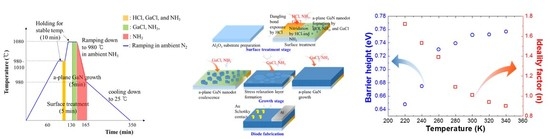
2. Materials and Methods

Nonpolar a-plane GaN layers were grown on 2 inch (1-102) r-plane sapphire substrates (Iljin display, Pyeongtaek, Korea), using a vertical-type homemade HVPE. The configuration of the homemade HVPE system was detailed elsewhere [11]. The stress relaxation layers using GaN nanodots were grown on r-plane sapphire substrates to prevent significant stress evolution during a-plane GaN growth. To achieve this, the substrates were subjected to a surface treatment before nonpolar GaN growth. This was composed of HCl etching (flow rate: 70 sccm) and nitridation with NH3 gas (flow rate: 2500 sccm) for 5 min. This treatment resulted in the formation of a discontinuous a-plane GaN nanodot buffer layer on the substrates (see Figure S1). Subsequently, a-plane GaN layers were grown on the a-plane GaN nanodot buffer layer via the reaction between GaCl and NH3 under atmospheric pressure and a temperature of ~1080 °C. HCl gas (flow rate: 40 sccm) was reacted with liquid Ga metal to form GaCl gas, which was transported to the growth zone where it reacted with NH3. The total flow rate of N2 used as the carrier gas was 15,000 sccm and the V/III ratio was approximately 6. Finally, 5 µm thick nonpolar a-plane GaN templates were obtained. Detailed procedures are presented in Figure 1a, and in other literature [16]. The growth kinetics are also explained elsewhere [19]. The densities of stacking fault and threading dislocation were 4.12 × 10⁵/cm, and 3.86 × 10⁹/cm2, respectively (not shown in this paper). These values are comparable to those of templates grown by MOCVD [20,21].
For the electrical characterization of HVPE a-plane GaN templates grown via GaN nanodot formation, Schottky diodes were fabricated using Au and Al metallization. First, 150 nm thick and 3 mm diameter Al metal was deposited on the a-plane GaN layers as ohmic contacts using a thermal evaporator (Infinity vacuum, Seoul, Korea). Then, the ohmic contacts were annealed at 550 °C in ambient Ar to improve the ohmic contact formation. Subsequently, Schottky contacts with 300 µm diameters were fabricated by an electron beam evaporator (Sorona, Seoul, Korea) using Au (40 nm) on the a-plane GaN layers, followed by rapid thermal annealing in ambient Ar at 550 °C. The details are presented in Figure 1b.

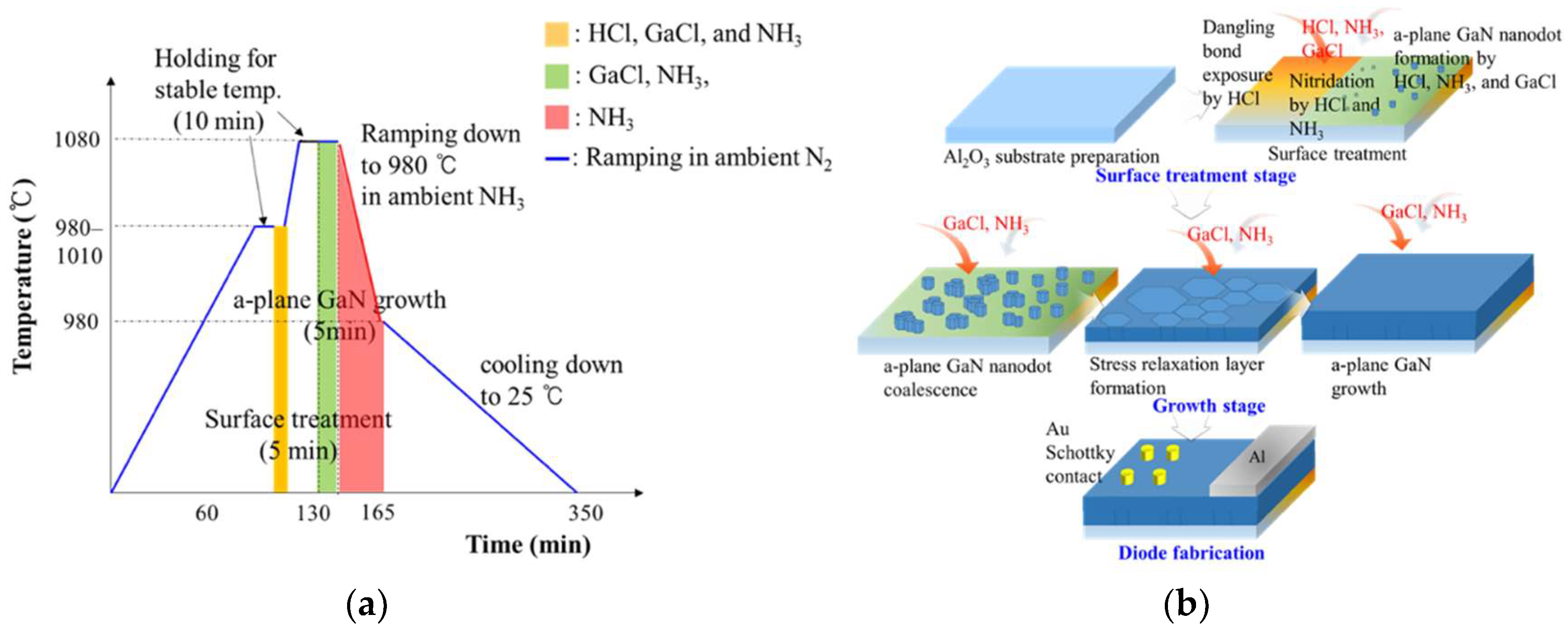
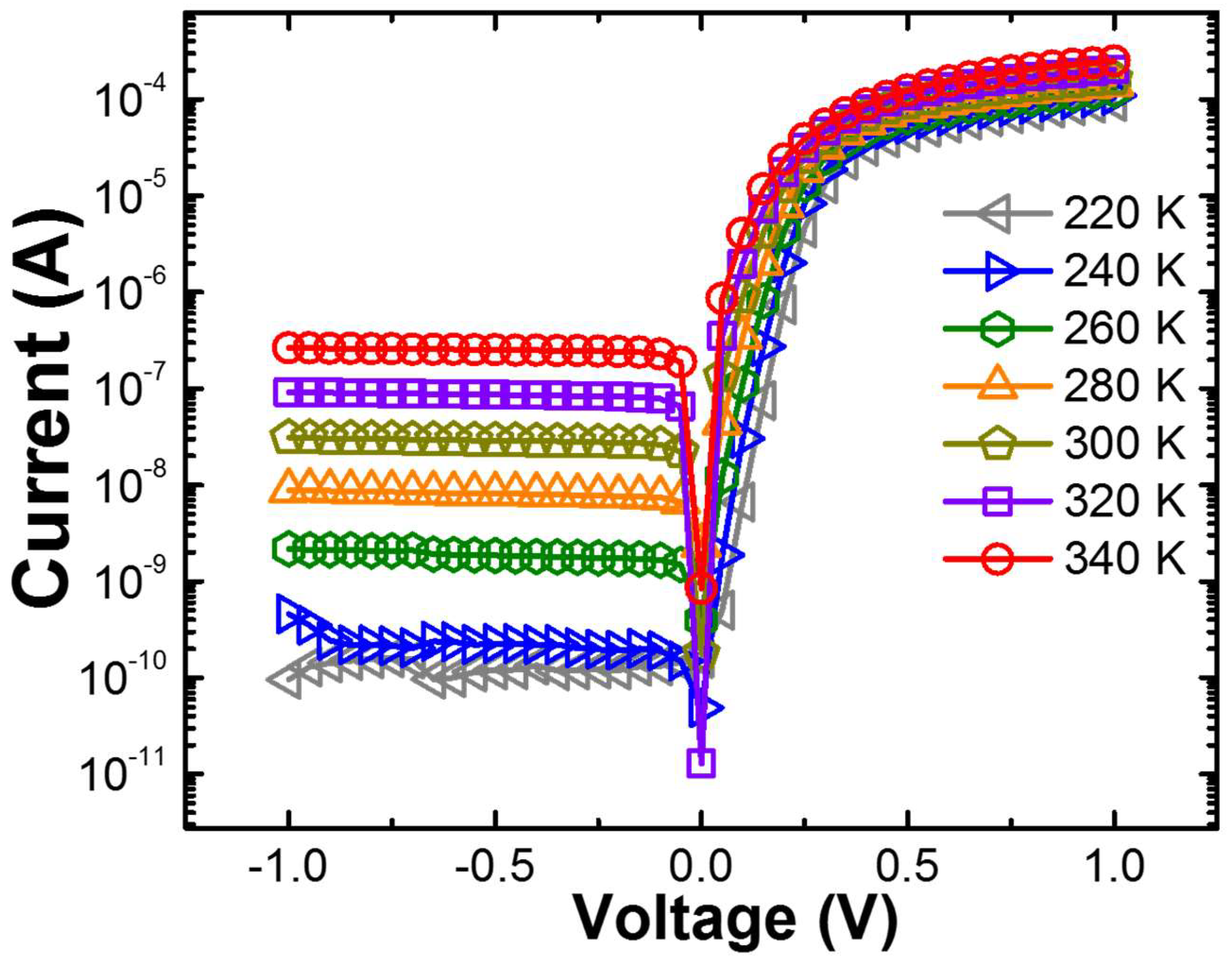
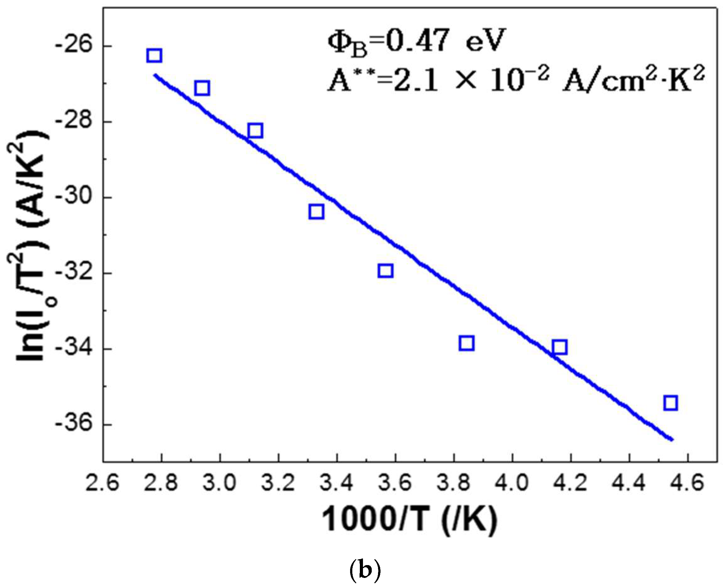
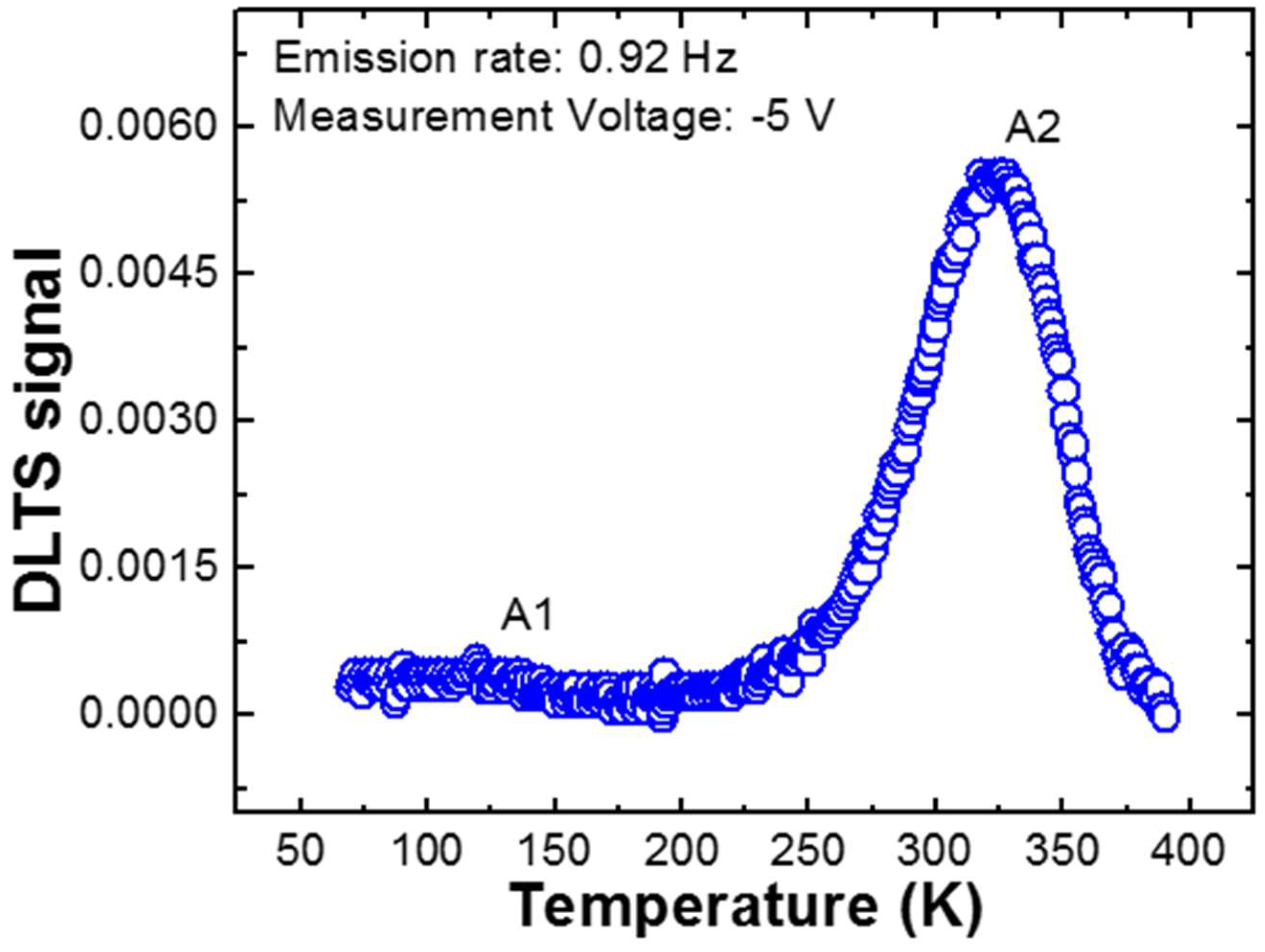
3. Results and Discussion

The forward and reverse current–voltage (IV) characteristics of the Schottky diodes formed on a-plane GaN templates grown via GaN nanodot formation in the temperature range from 220 to 340 K are plotted in Figure 2. The forward bias in the current–voltage–temperature (IVT) curves exhibits a linear behavior at low forward bias voltages but deviates considerably over 0.4 V from linearity due to the series resistance (Rs) in the whole temperature range. It is well known that thermally generated current carriers accelerate the larger current flow through the diode [22]. On the other hand, the reverse bias clearly shows excellent rectifying characteristics in the temperature range of 140–220 K, suggesting that Schottky junctions are well formed at the Au/a-plane GaN templates. Even though the rectification characteristics of the diodes decrease over 260 K, the ratios of the forward to reverse current at ±1 V of the Au/a-plane GaN template Schottky diodes in the entire temperature region were from 6.06 × 10⁴ to 1.59 × 10⁷, indicating a good rectification behavior.
The electrical parameters were extracted on the basis of the thermionic emission (TE) theory as follows [23,24]:
I = A A T 2 exp ( q Φ B k T ) [ exp ( q V n k T ) 1 ]   for   V     3 k T / q
I 0 = A A T 2 exp ( q Φ B k T )
where I0, A, A**, k, T, q, n, ΦB, and V represent the saturation current, contact area, Richardson constant (26.4 A·cm−2·K−2 for n-type GaN), Boltzmann constant, temperature, electron charge, ideality factor, Schottky barrier height, and applied voltage, respectively.
The measured barrier heights and ideality factors are listed in Figure 3a. It is worth noting that at ~260 K, the gradient of the barrier height and ideality factor significantly changed with the temperature gradient. This is a commonly observed phenomenon in Schottky diodes, and is attributed to the inhomogeneity of the barrier height in the contact [25]. Taking into consideration the current transport across the metal/semiconductor interface with a temperature-activated process, the dominant electrons flowing at low temperature exist at the lower Schottky barrier height because they cannot surmount the higher Schottky barrier height. However, at high temperature, electrons with sufficient energy can overcome the high Schottky barrier height, thereby increasing the dominant barrier height [26]. When applying the TE model, the ideality factors are varied from 0.88 to 1.74 in the temperature range of 220–340 K. From the slope of the Richardson plot, the barrier height corresponding to the activation energy was obtained in the temperature range from 220 K to 340 K, as seen in Figure 3b. We extracted 0.47 eV, a barrier height of 2.1 × 10⁻² A/cm2·K2 and the Richardson constant from the linear fit to the plot. It is interesting to note that the ΦB obtained from the figure is much smaller than the value of the TE model. The Richardson constant deviated by a decrease of almost three orders of magnitude from the theoretical value of 26.4 A/cm2·K2 for n-GaN. This can be explained by the spatially fluctuated barrier height in the contacts between the Au metal and a-plane GaN templates grown via GaN nanodot formation [27,28]. These results clearly suggest the formation of an inhomogeneity of ΦB on the Au/a-plane GaN templates grown via GaN nanodot formation, which can be attributed to the surface defects in nonpolar a-plane GaN [29,30,31].
It is essential to note that the higher deviation of ideality factors from unity at low temperature, even including inhomogeneous Schottky barrier heights, indicate that TE is not the only mechanism for the current transport. Note that the value of n is the measure of the extent to which the properties of a diode resemble the ideal diode characteristics and reflect the current transport mechanism in a device [32,33]. Other conduction mechanisms, such as thermionic field emission (TFE), field emission (FE), multistep tunneling via interface state, or dislocations, can be alternatives [34]. Considering that the TFE dominates the charge transport with a deviated ideality factor, the transport mechanism is given by [35]
I = I 0 exp ( q V E 00 coth ( E 00 / k T ) ) = I 0 exp ( q V E 0 )
I 0 = A A T π E 00 q ( Φ B V ξ ) k c o s h ( E 00 / k T ) × exp ( q ξ k T q ( Φ B ξ ) E 00 coth ( E 00 / k T ) )
where E00 = (/2)(ND/m*ɛs)1/2 is the characteristic energy related to the tunneling probability of potential barrier; E0 = E00coth(E00/kT); V is the applied bias voltage; ξ is equal to EC−EF, corresponding to kT/qln(NC/ND), where NC is the effective density of states in the conduction band (NC = 2.53 × 1018 cm−3 in GaN) [36]; h is Planck’s constant; m* is the effective mass; and ɛs is the dielectric constant.
The Schottky barrier heights and ideality factors in the temperature range from 220 to 340 K were estimated to be 0.87–1.48 eV and 0.88–1.34 respectively. (See Figure S2) Note that the ideality factors obtained from the TFE model are closer to unity, compared with those from the TE model. This verifies that the TFE, namely, Poole–Frenkel emission, is more appropriate to explain the current transport mechanism of HVPE a-plane GaN Schottky diodes formed through in situ nanodot formation over the entire range of measured temperatures. This behaviour is not different from the transport process of Schottky contacts to c- and a-plane GaN grown using other methods [17,18,37]. In addition, the Schottky barrier characteristics are comparable to those using the same contact material and similar diode fabrication conditions [38,39].
Even though the TFE model explains the current transport mechanism of HVPE a-plane GaN grown via nanodot formation well, one can observe the slight deviation of ideality factors from unity. Obviously, tunneling and high series resistance in the high voltage region can result in the inhomogeneity of ΦB. Also, the interface states are responsible for band bending, and behave as trap-assisted tunneling sites, giving rise to an increased ideality factor [34,40]. In addition, it is well known that HVPE a-plane GaN layers are prone to the formation of nitrogen desorption, nitrogen-related surface states, complex defects with VGa such as VN-VGa, and nitrogen anti-sites (NGa) during growth [41,42]. This encourages the tunneling process through the barrier, thus distorting the ideal Schottky characteristics. To elucidate the effects on unintentional charge traps, we performed deep-level transient spectroscopy (DLTS) measurements at a reverse voltage of 5 V in the temperature range of 70–370 K, as shown in Figure 4. We can clearly observe the two deep trap sites from the plateau. These trap levels exist at ~0.2 eV and ~0.55 eV below the conduction band edge. These are related to the noninteracting point defects [41,43,44,45]. These electronic deep trap carriers were filled at low temperature and released at over 260 K, thus increasing ϕB. Note that the DLTS signal abruptly starts to increase around 260 K. Therefore, we are assured that deep-level defects within the a-plane GaN template grown via in situ nanodot formation can be one of the important sources causing variation in ΦB and n for the two linear fitting regions around 260 K, confirmed by DLTS at different energy levels below the conduction band edge as shown in Figure 4. It is noticeable that the characteristics of the unintentional charge traps embedded in the a-plane GaN template grown via in situ nanodot formation are comparable to those of a-plane GaN layers grown using other methods [46,47]. This indicates that the a-plane GaN templates grown via in situ nanodot formation possess a great throughput advantage for various applications, compared to those grown using other methods. Table 1 summarizes the activation energy, capture cross section, and trap density obtained by DLTS analysis.

4. Conclusions

I–V–T measurements, conduction models, and DLTS analysis have been employed to investigate the electrical characteristics of Schottky diodes fabricated on HVPE a-plane GaN templates grown using in situ GaN nanodot formation. The barrier height and ideality factors are highly dependent upon the temperature gradient. Deviated ideality factors from unity reveal the inhomogeneity of the barrier height, which was confirmed by conventional Richardson, barrier height, and ideality plots. Also, we confirmed that TFE conduction is more appropriate to explain the current transport mechanism of HVPE a-plane GaN Schottky diodes grown via in situ nanodot formation, compared with the TE model. Furthermore, DLTS measurements suggest that defect-assisted tunneling played an important role in the Au/HVPE a-plane GaN Schottky contacts due to the presence of noninteracting point defects. The electrical characteristics of a-plane GaN templates grown using in situ nanodot formation are comparable to those of Schottky contacts to a-plane GaN layers grown using other methods. We believe that the formation of Au/HVPE a-plane GaN Schottky diodes based on in situ nanodot growth is promising for the application of nonpolar GaN-based opto-electrical devices.

Supplementary Materials

The following are available online at https://www.mdpi.com/2079-4991/8/6/397/s1. Figure S1: Plan-view SEM image of a-plane GaN nanodots formed on r-plane sapphire substrate after in situ surface treatment. Figure S2: Barrier height and ideality factor versus temperature in Au/HVPE a-plane GaN templates formed by in situ nanodot formation based on TFE model.

Author Contributions

M.L. performed the GaN epitaxial growth, interpreted the IVT and DLTS measurements, and wrote the manuscript. T.K.O.V. and K.S.L. conducted IVT and DLTS measurements. E.K.K. and S.P. designed the experiments and conceived the idea. All authors discussed and reviewed the manuscript.

Funding

This research received no external funding.

Acknowledgments

This research was supported by the Basic Science Research Program through the National Research Foundation of Korea (NRF) funded by the Ministry of Education (2016R1A6A1A03012069), the Korea Institute of Energy Technology Evaluation and Planning (KETEP), and the Ministry of Trade, Industry, & Energy (MOTIE) of the Republic of Korea (No. 20163030013380).

Conflicts of Interest

The authors declare no conflict of interest.

References

  1. Tang, F.; Zhu, T.; Oehler, F.; Fu, W.Y.; Griffiths, J.T.; Massabuau, F.C.-P.; Kappers, M.J.; Martin, T.L.; Bagot, P.A.; Moody, M.P. Indium clustering in a-plane InGaN quantum wells as evidenced by atom probe tomography. Appl. Phys. Lett. 2015, 106, 072104. [Google Scholar] [CrossRef]
  2. Jang, S.; Jung, S.; Park, J.; Kim, S.; Baik, K.H. Terahertz dielectric response of nonpolar a-plane GaN films. ECS Trans. 2017, 77, 127–131. [Google Scholar] [CrossRef]
  3. Sugiyama, T.; Honda, Y.; Yamaguchi, M.; Amano, H.; Isobe, Y.; Iwaya, M.; Takeuchi, T.; Kamiyama, S.; Akasaki, I.; Imade, M. Small current collapse in AlGaN/GaN HFETs on a-plane GaN self-standing substrate. Phys. Status Solidi (c) 2012, 9, 875–878. [Google Scholar] [CrossRef]
  4. Isobe, Y.; Ikki, H.; Sakakibara, T.; Iwaya, M.; Takeuchi, T.; Kamiyama, S.; Akasaki, I.; Sugiyama, T.; Amano, H.; Imade, M. Nonpolar a-plane AlGaN/GaN heterostructure field-effect transistors grown on freestanding GaN substrate. Appl. Phys. Express 2011, 4, 064102. [Google Scholar] [CrossRef]
  5. Matocha, K.; Tilak, V.; Dunne, G. Comparison of metal-oxide-semiconductor capacitors on c-and m-plane gallium nitride. Appl. Phys. lett. 2007, 90, 123511. [Google Scholar] [CrossRef]
  6. Wang, Y.-L.; Ren, F.; Lim, W.; Pearton, S.; Baik, K.H.; Hwang, S.-M.; Seo, Y.G.; Jang, S. Hydrogen sensing characteristics of non-polar a-plane GaN schottky diodes. Curr. Appl. Phys. 2010, 10, 1029–1032. [Google Scholar] [CrossRef]
  7. Rudziński, M.; Kudrawiec, R.; Patriarche, G.; Kucharski, R.; Caban, P.; Strupiński, W. Simultaneous growth of GaN/AlGaN quantum wells on c-, a-, m-, and (20.1)-plane GaN bulk substrates obtained by the ammonothermal method: Structural studies. J. Cryst. Growth 2015, 414, 87–93. [Google Scholar] [CrossRef]
  8. Zhang, J.; Tian, W.; Wu, F.; Wan, Q.; Wang, Z.; Zhang, J.; Li, Y.; Dai, J.; Fang, Y.; Wu, Z. The effects of substrate nitridation on the growth of nonpolar a-plane GaN on r-plane sapphire by metalorganic chemical vapor deposition. Appl. Surf. Sci. 2014, 307, 525–532. [Google Scholar] [CrossRef]
  9. Ryu, S.R.; Ram, S.G.; Kwon, Y.H.; Yang, W.C.; Kim, S.H.; Woo, Y.D.; Shin, S.H.; Kang, T.W. HVPE growth of self-aligned gan nanorods on c-plane, a-plane, r-plane, and m-plane sapphire wafers. J. Mater. Sci. 2015, 50, 6260–6267. [Google Scholar] [CrossRef]
  10. Moldawer, A.; Bhattacharyya, A.; Zhou, L.; Smith, D.J.; Moustakas, T.D. Characterization of a-plane GaN templates grown by hvpe and high efficiency deep uv emitting AlGaN/AlN MQWs grown by MBE on such templates. Phys. Status Solidi (c) 2014, 11, 585–589. [Google Scholar] [CrossRef]
  11. Lee, M.; Mikulik, D.; Yang, M.; Park, S. Nearly perfect GaN crystal via pit-assisted growth by HVPE. CrystEngComm 2017, 19, 2036–2041. [Google Scholar] [CrossRef]
  12. Amilusik, M.; Sochacki, T.; Lucznik, B.; Fijalkowski, M.; Iwinska, M.; Weyher, J.; Grzanka, E.; Krupczynska, P.; Khachapuridze, A.; Grzegory, I. Homoepitaxial HVPE GaN growth on non-and semi-polar seeds. J. Cryst. Growth 2015, 403, 48–54. [Google Scholar] [CrossRef]
  13. Kong, B.H.; Sun, Q.; Han, J.; Lee, I.-H.; Cho, H.K. Classification of stacking faults and dislocations observed in nonpolar a-plane GaN epilayers using transmission electron microscopy. Appl. Surf. Sci. 2012, 258, 2522–2528. [Google Scholar] [CrossRef]
  14. Paskova, T.; Kroeger, R.; Paskov, P.; Figge, S.; Hommel, D.; Monemar, B.; Haskell, B.; Fini, P.; Speck, J.; Nakamura, S. Microscopic emission properties of nonpolar α-plane GaN grown by HVPE. In Gallium Nitride Materials and Devices; International Society for Optics and Photonics: Bellingham, WA, USA, 2006; p. 612106. [Google Scholar]
  15. Wu, Y.-H.; Lee, C.-H.; Chu, C.-M.; Yeh, Y.-H.; Chen, C.-L.; Lee, W.-I. A simple growth method to produce a-plane GaN thick films by hydride vapor phase epitaxy. Jpn. J. Appl. Phys. 2013, 52, 08JB08. [Google Scholar] [CrossRef]
  16. Lee, M.; Mikulik, D.; Park, S. Thick GaN growth via gan nanodot formation by HVPE. CrystEngComm 2017, 19, 930–935. [Google Scholar] [CrossRef]
  17. Phark, S.-H.; Kim, H.; Song, K.M.; Kang, P.G.; Shin, H.S.; Kim, D.-W. Current transport in Pt schottky contacts to a-plane n-type GaN. J. Phys. D Appl. Phys. 2010, 43, 165102. [Google Scholar] [CrossRef]
  18. Kim, H.; Lee, S.-N.; Park, Y.; Kwak, J.S.; Seong, T.-Y. Metallization contacts to nonpolar a-plane n-type GaN. Appl. Phys. Lett. 2008, 93, 032105. [Google Scholar] [CrossRef]
  19. Schwartzkopf, M.; Buffet, A.; Körstgens, V.; Metwalli, E.; Schlage, K.; Benecke, G.; Perlich, J.; Rawolle, M.; Rothkirch, A.; Heidmann, B. From atoms to layers: In situ gold cluster growth kinetics during sputter deposition. Nanoscale 2013, 5, 5053–5062. [Google Scholar] [CrossRef] [PubMed]
  20. Imer, B.M.; Wu, F.; DenBaars, S.P.; Speck, J.S. Improved quality (11 2¯ 0) a-plane GaN with sidewall lateral epitaxial overgrowth. Appl. Phys. Lett. 2006, 88, 061908. [Google Scholar] [CrossRef]
  21. Moram, M.; Johnston, C.; Kappers, M.; Humphreys, C. Measuring dislocation densities in nonpolar a-plane GaN films using atomic force microscopy. J. Phys. D Appl. Phys. 2010, 43, 055303. [Google Scholar] [CrossRef]
  22. Taşçıoğlu, İ.; Aydemir, U.; Altındal, Ş.; Kınacı, B.; Özçelik, S. Analysis of the forward and reverse bias iv characteristics on Au/PVA: Zn/n-Si schottky barrier diodes in the wide temperature range. J. Appl. Phys. 2011, 109, 054502. [Google Scholar] [CrossRef]
  23. Kumar, A.; Arafin, S.; Amann, M.C.; Singh, R. Temperature dependence of electrical characteristics of Pt/GaN schottky diode fabricated by UHV e-beam evaporation. Nanoscale Res. Lett. 2013, 8, 481. [Google Scholar] [CrossRef] [PubMed]
  24. Peta, K.R.; Kim, M.D. Leakage current transport mechanism under reverse bias in Au/Ni/GaN schottky barrier diode. Superlattices Microstruct. 2017, 113, 678–683. [Google Scholar] [CrossRef]
  25. Iucolano, F.; Roccaforte, F.; Giannazzo, F.; Raineri, V. Barrier inhomogeneity and electrical properties of Pt/GaN schottky contacts. J. Appl. Phys. 2007, 102, 113701. [Google Scholar] [CrossRef]
  26. Rajpalke, M.K.; Bhat, T.N.; Roul, B.; Kumar, M.; Krupanidhi, S. Current transport in nonpolar a-plane InN/GaN heterostructures schottky junction. J. Appl. Phys. 2012, 112, 023706. [Google Scholar] [CrossRef]
  27. Song, Y.; Van Meirhaeghe, R.; Laflere, W.; Cardon, F. On the difference in apparent barrier height as obtained from capacitance-voltage and current-voltage-temperature measurements on Al/p-InP schottky barriers. Solid-State Electron. 1986, 29, 633–638. [Google Scholar] [CrossRef]
  28. Kwietniewski, N.; Sochacki, M.; Szmidt, J.; Guziewicz, M.; Kaminska, E.; Piotrowska, A. Influence of surface cleaning effects on properties of schottky diodes on 4H–SiC. Appl. Surf. Sci. 2008, 254, 8106–8110. [Google Scholar] [CrossRef]
  29. Kim, H.; Phark, S.H.; Song, K.M.; Kim, D.W. Electrical characterization of pt schottky contacts to a-plane n-type GaN. In AIP Conference Proceedings; AIP: Melville, NY, USA, 2011; pp. 923–924. [Google Scholar]
  30. Yu, L.; Liu, Q.; Xing, Q.; Qiao, D.; Lau, S.; Redwing, J. The role of the tunneling component in the current–voltage characteristics of metal-GaN schottky diodes. J. Appl. Phys. 1998, 84, 2099–2104. [Google Scholar] [CrossRef]
  31. Jang, J.-S.; Kim, D.; Seong, T.-Y. Schottky barrier characteristics of Pt contacts to n-type InGaN. J. Appl. Phys. 2006, 99, 073704. [Google Scholar] [CrossRef]
  32. Zhi, T.; Tao, T.; Liu, B.; Li, Y.; Zhuang, Z.; Zhang, G.; Xie, Z.; Zhang, R.; Zheng, Y. Asymmetric tunneling model of forward leakage current in GaN/InGaN light emitting diodes. AIP Adv. 2015, 5, 087151. [Google Scholar] [CrossRef] [Green Version]
  33. Sze, S. Physics of Semiconductors Devices; John Wiley & Son: Hoboken, NJ, USA, 2006. [Google Scholar]
  34. Faraz, S.; Willander, M.; Wahab, Q. Interface state density distribution in Au/n-ZnO nanorods schottky diodes. In IOP Conference Series: Materials Science and Engineering; IOP Publishing: Bristol, UK, 2012; p. 012006. [Google Scholar]
  35. Padovani, F.; Stratton, R. Field and thermionic-field emission in schottky barriers. Solid-State Electron. 1966, 9, 695–707. [Google Scholar] [CrossRef]
  36. Hacke, P.; Detchprohm, T.; Hiramatsu, K.; Sawaki, N. Schottky barrier on n-type GaN grown by hydride vapor phase epitaxy. Appl. Phys. Lett. 1993, 63, 2676–2678. [Google Scholar] [CrossRef]
  37. Miller, E.; Yu, E.; Waltereit, P.; Speck, J. Analysis of reverse-bias leakage current mechanisms in GaN grown by molecular-beam epitaxy. Appl. Phys. Lett. 2004, 84, 535–537. [Google Scholar] [CrossRef]
  38. Diale, M.; Auret, F.D. Effects of chemical treatment on barrier height and ideality factors of Au/GaN schottky diodes. Phys. B Condens. Matter 2009, 404, 4415–4418. [Google Scholar] [CrossRef]
  39. Janardhanam, V.; Jyothi, I.; Lee, J.-H.; Kim, J.-Y.; Reddy, V.R.; Choi, C.-J. Electrical properties and carrier transport mechanism of Au/n-GaN schottky contact modified using a copper pthalocyanine (CuPc) interlayer. Mater. Trans. 2014, 55, 758–762. [Google Scholar] [CrossRef]
  40. Garg, M.; Kumar, A.; Nagarajan, S.; Sopanen, M.; Singh, R. Investigation of significantly high barrier height in Cu/GaN schottky diode. AIP Adv. 2016, 6, 015206. [Google Scholar] [CrossRef]
  41. Fang, Z.-Q.; Look, D.C.; Jasinski, J.; Benamara, M.; Liliental-Weber, Z.; Molnar, R.J. Evolution of deep centers in GaN grown by hydride vapor phase epitaxy. Appl. Phys. Lett. 2001, 78, 332–334. [Google Scholar] [CrossRef] [Green Version]
  42. Takahashi, K.; Yoshikawa, A.; Sandhu, A. Wide Bandgap Semiconductors; Springer: Berlin/Heidelberg, Germany, 2007; p. 239. [Google Scholar]
  43. Cho, H.; Kim, C.; Hong, C.-H. Electron capture behaviors of deep level traps in unintentionally doped and intentionally doped n-type GaN. J. Appl. Phys. 2003, 94, 1485–1489. [Google Scholar] [CrossRef]
  44. Look, D.C.; Fang, Z.-Q.; Claflin, B. Identification of donors, acceptors, and traps in bulk-like HVPE GaN. J. Cryst. Growth 2005, 281, 143–150. [Google Scholar] [CrossRef]
  45. Armstrong, A.; Arehart, A.; Green, D.; Mishra, U.; Speck, J.; Ringel, S. Impact of deep levels on the electrical conductivity and luminescence of gallium nitride codoped with carbon and silicon. J. Appl. Phys. 2005, 98, 053704. [Google Scholar] [CrossRef]
  46. Pak, S.W.; Lee, D.U.; Kim, E.K.; Park, S.H.; Joo, K.; Yoon, E. Defect states of a-plane GaN grown on r-plane sapphire by controlled integration of silica nano-spheres. J. Cryst. Growth 2013, 370, 78–81. [Google Scholar] [CrossRef]
  47. Song, H.; Kim, E.K.; Baik, K.H.; Hwang, S.-M.; Jang, Y.W.; Lee, J.Y. Characterization of deep levels in a-plane GaN epi-layers grown using various growth techniques. J. Cryst. Growth 2012, 340, 23–27. [Google Scholar] [CrossRef]
Figure 1. Schematic illustrations of (a) the growth sequence of a-plane GaN templates via in situ nanodot formation and (b) the fabrication of hydride vapor phase epitaxy (HVPE) a-plane GaN Schottky diodes based on the suggested method.
Nanomaterials 08 00397 g001
Figure 2. Temperature-dependent IV characteristics of Au/a-plane GaN templates grown via GaN nanodot formation.
Nanomaterials 08 00397 g002
Figure 3. (a) Barrier height and ideality factor versus temperature in Au/HVPE a-plane GaN templates formed by in situ nanodot formation; (b) Richardson plot of ln(I0/T2) versus 1000/T for Au/HVPE a-plane GaN Schottky contact.
Nanomaterials 08 00397 g003aNanomaterials 08 00397 g003b
Figure 4. Deep-level transient spectroscopy (DLTS) spectrum of Au/HVPE a-plane GaN template Schottky diodes grown via in situ nanodot formation, measured at a reverse voltage of −5 V in the temperature range of 70–370 K.
Nanomaterials 08 00397 g004
Table 1. Defect parameters for Au/a-plane GaN Schottky diodes.
Ref.DefectActivation Energy (eV)Capture Cross Section (cm2)Trap Density (cm−3)
This studyA10.201.14 × 10−175 × 1012
A20.554.4 × 10−174.7 × 10¹³
[42]E10.235.43 × 10−159.5 × 10¹³
E20.54.65 × 10−172.3 × 10¹⁴
[45]EA10.569.72 × 10−163 × 1013
[46]E30.588.9 × 10−123.8 × 10¹⁴

