Transport and Field Emission Properties of MoS2 Bilayers

 ,
,  ,
,  ,
,  and
and 
Abstract
1. Introduction
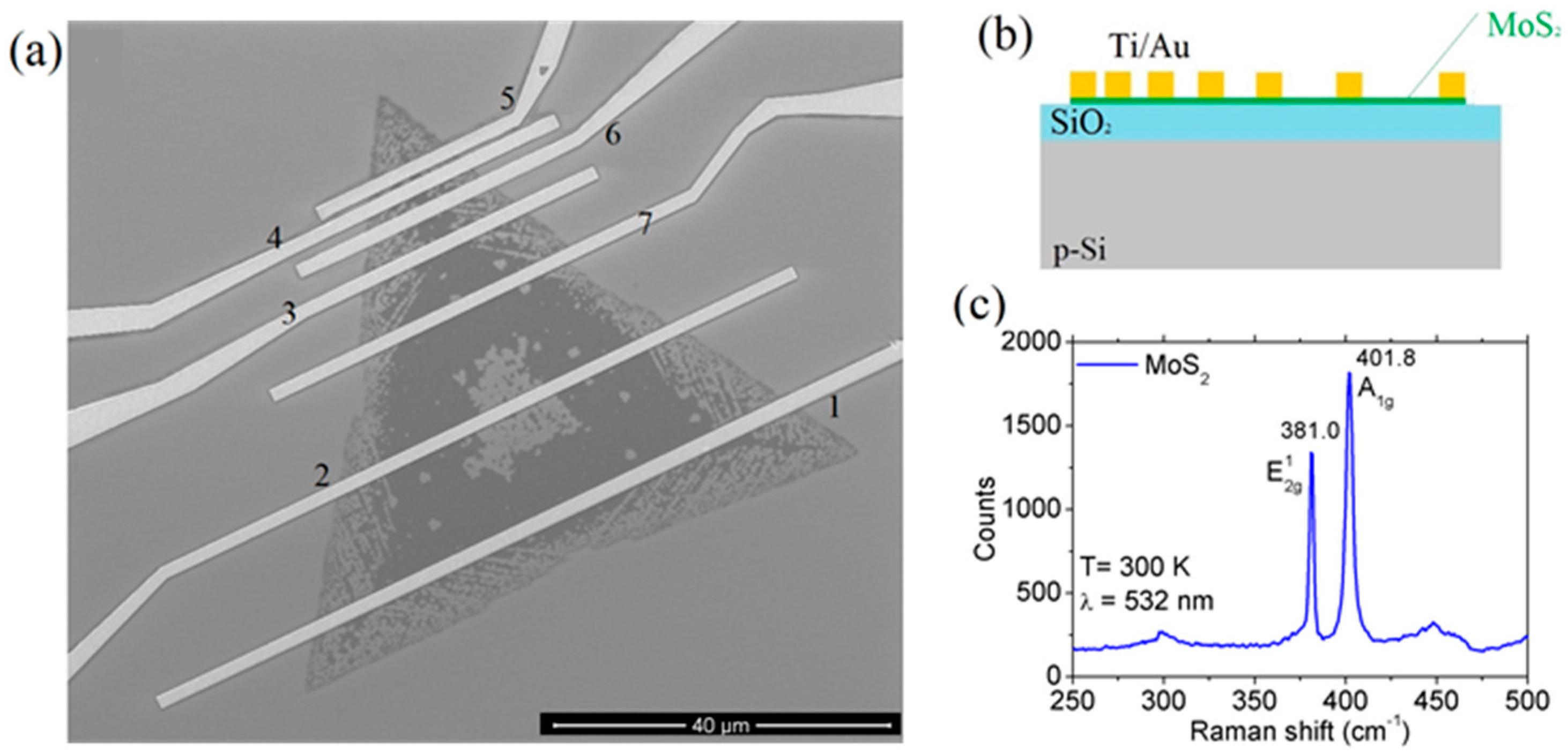
2. Materials and Methods
3. Results
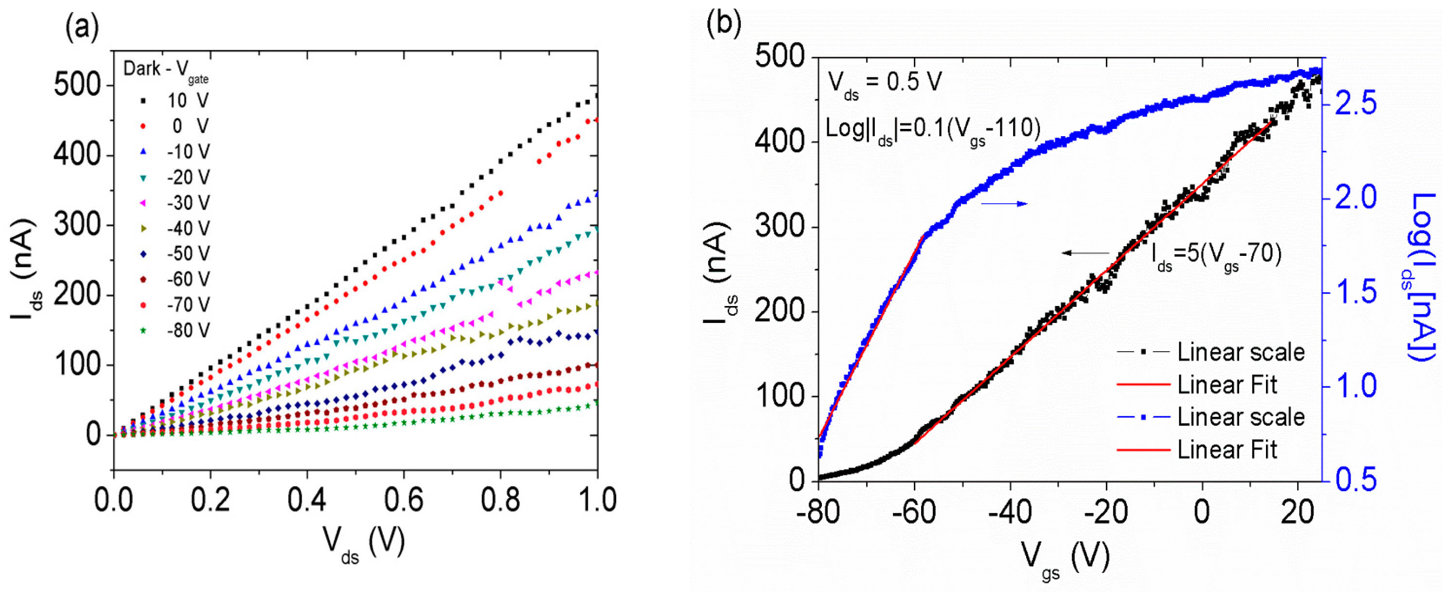
3.1. Transistor Characterization
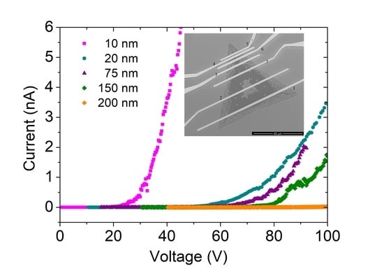
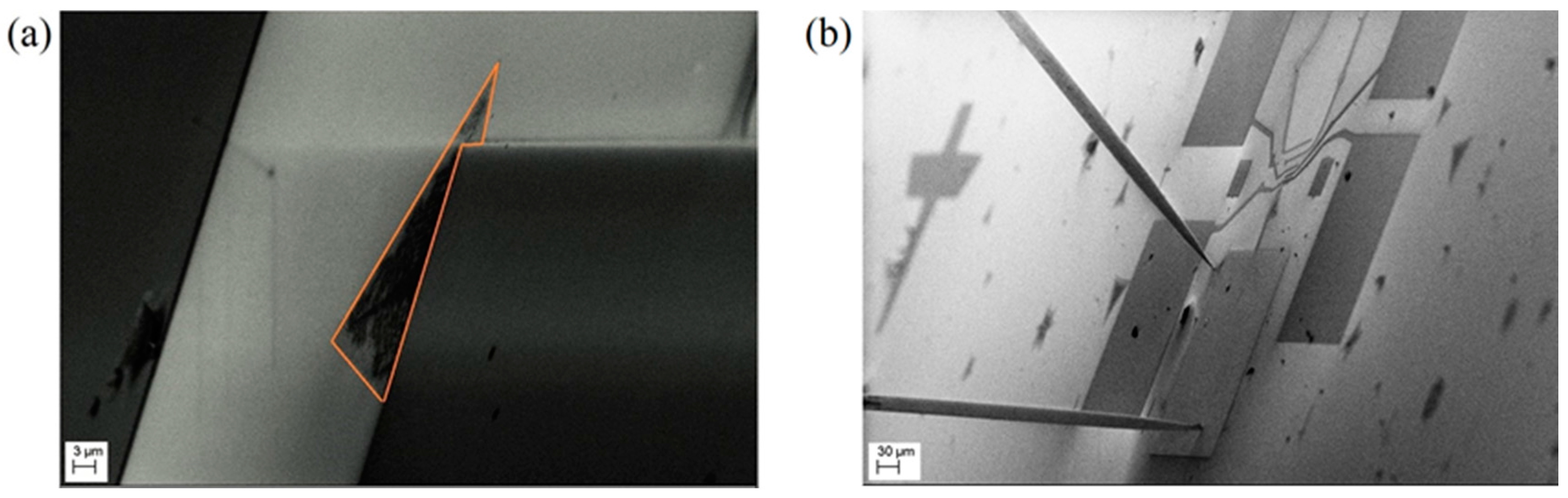
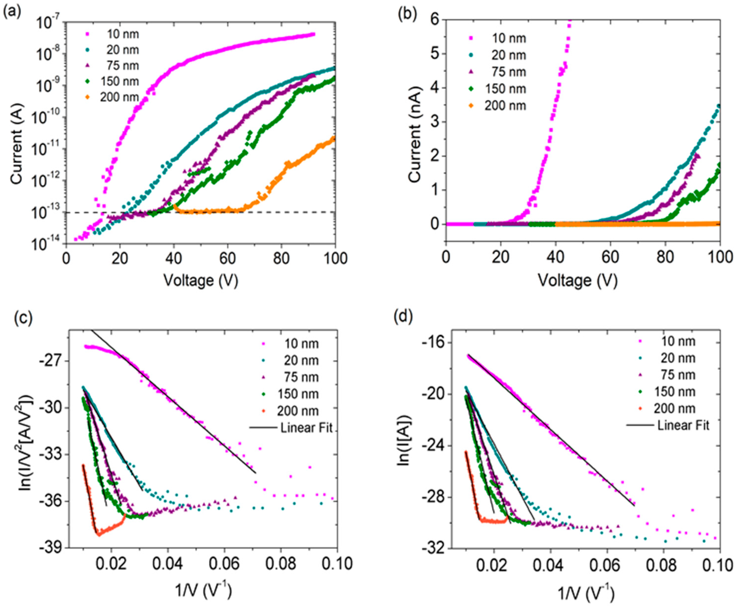
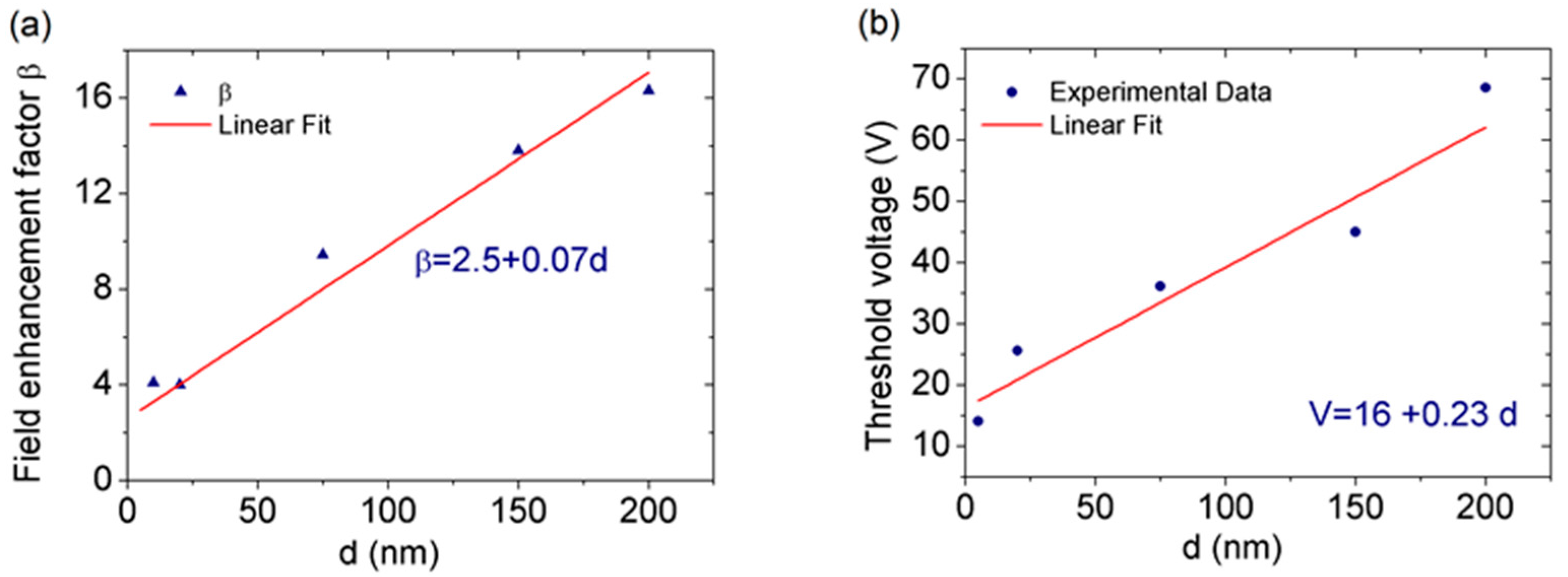
3.2. Field Emission Measurements
4. Conclusions
Acknowledgments
Author Contributions
Conflicts of Interest
References
- Schwierz, F. Graphene transistors. Nat. Nanotechnol. 2010, 5, 487–496. [Google Scholar] [CrossRef] [PubMed]
- Avouris, P. Graphene: Electronic and Photonic Properties and Devices. Nano Lett. 2010, 10, 4285–4294. [Google Scholar] [CrossRef] [PubMed]
- Di Bartolomeo, A.; Giubileo, F.; Iemmo, L.; Romeo, F.; Santandrea, S.; Gambardella, U. Transfer characteristics and contact resistance in Ni- and Ti-contacted graphene-based field-effect transistors. J. Phys. Condens. Matter 2013, 25, 155303. [Google Scholar] [CrossRef] [PubMed]
- Di Bartolomeo, A.; Giubileo, F.; Romeo, F.; Sabatino, P.; Carapella, G.; Iemmo, L.; Schroeder, T.; Lupina, G. Graphene field effect transistors with niobium contacts and asymmetric transfer characteristics. Nanotechnology 2015, 26, 475202. [Google Scholar] [CrossRef] [PubMed]
- Zhou, Z.; Yap, Y.K. Two-Dimensional Electronics and Optoelectronics: Present and Future. Electronics 2017, 6, 53. [Google Scholar] [CrossRef]
- Lin, Z.; McCreary, A.; Briggs, N.; Subramanian, S.; Zhang, K.; Sun, Y.; Li, X.; Borys, N.J.; Yuan, H.; Fullerton-Shirey, S.K.; et al. 2D materials advances: From large scale synthesis and controlled heterostructures to improved characterization techniques, defects and applications. 2D Mater. 2016, 3, 042001. [Google Scholar] [CrossRef]
- Di Bartolomeo, A.; Genovese, L.; Giubileo, F.; Iemmo, L.; Luongo, G.; Foller, T.; Schleberger, M. Hysteresis in the transfer characteristics of MoS2 transistors. 2D Mater. 2018, 5, 015014. [Google Scholar] [CrossRef]
- Yoon, Y.; Ganapathi, K.; Salahuddin, S. How Good Can Monolayer MoS2 Transistors Be? Nano Lett. 2011, 11, 3768–3773. [Google Scholar] [CrossRef] [PubMed]
- Late, D.J.; Shaikh, P.A.; Khare, R.; Kashid, R.V.; Chaudhary, M.; More, M.A.; Ogale, S.B. Pulsed Laser-Deposited MoS2 Thin Films on W and Si: Field Emission and Photoresponse Studies. ACS Appl. Mater. Interfaces 2014, 6, 15881–15888. [Google Scholar] [CrossRef] [PubMed]
- Lopez-Sanchez, O.; Lembke, D.; Kayci, M.; Radenovic, A.; Kis, A. Ultrasensitive photodetectors based on monolayer MoS2. Nat. Nanotechnol. 2013, 8, 497. [Google Scholar] [CrossRef] [PubMed]
- Feng, Y.; Zhang, K.; Wang, F.; Liu, Z.; Fang, M.; Cao, R.; Miao, Y.; Yang, Z.; Mi, W.; Han, Y.; et al. Synthesis of Large-Area Highly Crystalline Monolayer Molybdenum Disulfide with Tunable Grain Size in a H2 Atmosphere. ACS Appl. Mater. Interfaces 2015, 7, 22587–22593. [Google Scholar] [CrossRef] [PubMed]
- Mak, K.F.; Lee, C.; Hone, J.; Shan, J.; Heinz, T.F. Atomically Thin MoS2: A New Direct-Gap Semiconductor. Phys. Rev. Lett. 2010, 105, 136805. [Google Scholar] [CrossRef] [PubMed]
- Zhou, C.; Wang, X.; Raju, S.; Lin, Z.; Villaroman, D.; Huang, B.; Chan, H.L.-W.; Chan, M.; Chai, Y. Low voltage and high ON/OFF ratio field-effect transistors based on CVD MoS2 and ultra high-k gate dielectric PZT. Nanoscale 2015, 7, 8695–8700. [Google Scholar] [CrossRef] [PubMed]
- Nourbakhsh, A.; Zubair, A.; Joglekar, S.; Dresselhaus, M.; Palacios, T. Subthreshold swing improvement in MoS2 transistors by the negative-capacitance effect in a ferroelectric Al-doped-HfO2/HfO2 gate dielectric stack. Nanoscale 2017, 9, 6122–6127. [Google Scholar] [CrossRef] [PubMed]
- Radisavljevic, B.; Radenovic, A.; Brivio, J.; Giacometti, V.; Kis, A. Single-layer MoS2 transistors. Nat. Nanotechnol. 2011, 6, 147–150. [Google Scholar] [CrossRef] [PubMed]
- Di Bartolomeo, A.; Genovese, L.; Foller, T.; Giubileo, F.; Luongo, G.; Croin, L.; Liang, S.-J.; Ang, L.K.; Schleberger, M. Electrical transport and persistent photoconductivity in monolayer MoS2 phototransistors. Nanotechnology 2017, 28, 214002. [Google Scholar] [CrossRef] [PubMed]
- Zibouche, N.; Kuc, A.; Musfeldt, J.; Heine, T. Transition-metal dichalcogenides for spintronic applications. Annalen der Physik 2014, 526, 395–401. [Google Scholar] [CrossRef]
- Han, W. Perspectives for spintronics in 2D materials. APL Mater. 2016, 4, 032401. [Google Scholar] [CrossRef]
- Lembke, D.; Allain, A.; Kis, A. Thickness-dependent mobility in two-dimensional MoS2 transistors. Nanoscale 2015, 7, 6255–6260. [Google Scholar] [CrossRef] [PubMed]
- Zhong, H.; Quhe, R.; Wang, Y.; Ni, Z.; Ye, M.; Song, Z.; Pan, Y.; Yang, J.; Yang, L.; Lei, M.; et al. Interfacial Properties of Monolayer and Bilayer MoS2 Contacts with Metals: Beyond the Energy Band Calculations. Sci. Rep. 2016, 6, 21786. [Google Scholar] [CrossRef] [PubMed]
- Fowler, R.H.; Nordheim, L. Electron emission in intense electric fields. Proc. R. Soc. Lond. A 1928, 119, 173–181. [Google Scholar] [CrossRef]
- Spindt, C.A.; Holland, C.E.; Rosengreen, A.; Brodie, I. Field-emitter arrays for vacuum microelectronics. IEEE Trans. Electron Dev. 1991, 38, 2355–2363. [Google Scholar] [CrossRef]
- Di Bartolomeo, A.; Scarfato, A.; Giubileo, F.; Bobba, F.; Biasiucci, M.; Cucolo, A.M.; Santucci, S.; Passacantando, M. A local field emission study of partially aligned carbon-nanotubes by atomic force microscope probe. Carbon 2007, 45, 2957–2971. [Google Scholar] [CrossRef]
- Di Bartolomeo, A.; Passacantando, M.; Niu, G.; Schlykow, V.; Lupina, G.; Giubileo, F.; Schroeder, T. Observation of field emission from GeSn nanoparticles epitaxially grown on silicon nanopillar arrays. Nanotechnology 2016, 27, 485707. [Google Scholar] [CrossRef] [PubMed]
- Iemmo, L.; Di Bartolomeo, A.; Giubileo, F.; Luongo, G.; Passacantando, M.; Niu, G.; Hatami, F.; Skibitzki, O.; Schroeder, T. Graphene enhanced field emission from InP nanocrystals. Nanotechnology 2017, 28, 495705. [Google Scholar] [CrossRef] [PubMed]
- Joag, D.S.; More, M.A.; Sheini, F.J. Field Emission from Nanowires. In Nanowires—Implementations and Applications; Hashim, A., Ed.; InTech: Rijeka, Croatia, 2011. [Google Scholar]
- Lin, P.-H.; Sie, C.-L.; Chen, C.-A.; Chang, H.-C.; Shih, Y.-T.; Chang, H.-Y.; Su, W.-J.; Lee, K.-Y. Field Emission Characteristics of the Structure of Vertically Aligned Carbon Nanotube Bundles. Nanoscale Res. Lett. 2015, 10, 297. [Google Scholar] [CrossRef] [PubMed]
- Giubileo, F.; Di Bartolomeo, A.; Scarfato, A.; Iemmo, L.; Bobba, F.; Passacantando, M.; Santucci, S.; Cucolo, A.M. Local probing of the field emission stability of vertically aligned multi-walled carbon nanotubes. Carbon 2009, 47, 1074–1080. [Google Scholar] [CrossRef]
- Di, Y.; Xiao, M.; Zhang, X.; Wang, Q.; Li, C.; Lei, W.; Cui, Y. Large and stable emission current from synthesized carbon nanotube/fiber network. J. Appl. Phys. 2014, 115, 064305. [Google Scholar] [CrossRef]
- Giubileo, F.; Iemmo, L.; Luongo, G.; Martucciello, N.; Raimondo, M.; Guadagno, L.; Passacantando, M.; Lafdi, K.; Di Bartolomeo, A. Transport and field emission properties of buckypapers obtained from aligned carbon nanotubes. J. Mater. Sci. 2017, 52, 6459–6468. [Google Scholar] [CrossRef]
- Di Bartolomeo, A.; Giubileo, F.; Iemmo, L.; Romeo, F.; Russo, S.; Unal, S.; Passacantando, M.; Grossi, V.; Cucolo, A.M. Leakage and field emission in side-gate graphene field effect transistors. Appl. Phys. Lett. 2016, 109, 023510. [Google Scholar] [CrossRef]
- Suryawanshi, S.R.; More, M.A.; Late, D.J. Exfoliated 2D black phosphorus nanosheets: Field emission studies. J. Vac. Sci. Technol. B Nanotechnol. Microelectron. Mater. Process. Meas. Phenom. 2016, 34, 041803. [Google Scholar] [CrossRef]
- Giubileo, F.; Di Bartolomeo, A.; Iemmo, L.; Luongo, G.; Passacantando, M.; Koivusalo, E.; Hakkarainen, T.V.; Guina, M. Field Emission from Self-Catalyzed GaAs Nanowires. Nanomaterials 2017, 7. [Google Scholar] [CrossRef] [PubMed]
- Choi, W.B.; Chung, D.S.; Kang, J.H.; Kim, H.Y.; Jin, Y.W.; Han, I.T.; Lee, Y.H.; Jung, J.E.; Lee, N.S.; Park, G.S.; et al. Fully sealed, high-brightness carbon-nanotube field-emission display. Appl. Phys. Lett. 1999, 75, 3129–3131. [Google Scholar] [CrossRef]
- Yabushita, R.; Hata, K.; Sato, H.; Saito, Y. Development of compact field emission scanning electron microscope equipped with multiwalled carbon nanotube bundle cathode. J. Vac. Sci. Technol. B Nanotechnol. Microelectron. Nanometer Struct. Process. Meas. Phenom. 2007, 25, 640–642. [Google Scholar] [CrossRef]
- Cole, M.T.; Parmee, R.J.; Milne, W.I. Nanomaterial-based x-ray sources. Nanotechnology 2016, 27, 1–9. [Google Scholar] [CrossRef] [PubMed]
- Gupta, A.P.; Park, S.; Yeo, S.J.; Jung, J.; Cho, C.; Paik, S.H.; Park, H.; Cho, Y.C.; Kim, S.H.; Shin, J.H.; et al. Direct Synthesis of Carbon Nanotube Field Emitters on Metal Substrate for Open-Type X-ray Source in Medical Imaging. Materials 2017, 10, 878. [Google Scholar] [CrossRef] [PubMed]
- Kong, D.; Wang, H.; Cha, J.J.; Pasta, M.; Koski, K.J.; Yao, J.; Cui, Y. Synthesis of MoS2 and MoSe2 Films with Vertically Aligned Layers. Nano Lett. 2013, 13, 1341–1347. [Google Scholar] [CrossRef] [PubMed]
- Gaur, A.P.S.; Sahoo, S.; Mendoza, F.; Rivera, A.M.; Kumar, M.; Dash, S.P.; Morell, G.; Katiyar, R.S. Cold cathode emission studies on topographically modified few layer and single layer MoS2 films. Appl. Phys. Lett. 2016, 108, 043103. [Google Scholar] [CrossRef]
- Kashid, R.V.; Late, D.J.; Chou, S.S.; Huang, Y.-K.; De, M.; Joag, D.S.; More, M.A.; Dravid, V.P. Enhanced Field-Emission Behavior of Layered MoS2 Sheets. Small 2013, 9, 2730–2734. [Google Scholar] [CrossRef] [PubMed]
- Li, Y.B.; Bando, Y.; Golberg, D. MoS2 nanoflowers and their field-emission properties. Appl. Phys. Lett. 2003, 82, 1962–1964. [Google Scholar] [CrossRef]
- Sin Ang, Y.; Zubair, M.; Ooi, K.J.A.; Ang, L.K. Generalized Fowler-Nordheim field-induced vertical electron emission model for two-dimensional materials. arXiv, 2017; arXiv:1711.05898. [Google Scholar]
- Li, X.; Zhu, H. Two-dimensional MoS2: Properties, preparation, and applications. J. Materiomics 2015, 1, 33–44. [Google Scholar] [CrossRef]
- Guo, Y.; Robertson, J. Origin of the high work function and high conductivity of MoO3. Appl. Phys. Lett. 2014, 105, 222110. [Google Scholar] [CrossRef]
- Jariwala, D.; Sangwan, V.K.; Late, D.J.; Johns, J.E.; Dravid, V.P.; Marks, T.J.; Lauhon, L.J.; Hersam, M.C. Band-like transport in high mobility unencapsulated single-layer MoS2 transistors. Appl. Phys. Lett. 2013, 102, 173107. [Google Scholar] [CrossRef]
- Radisavljevic, B.; Kis, A. Mobility engineering and a metal–insulator transition in monolayer MoS2. Nat. Mater. 2013, 12, 815. [Google Scholar] [CrossRef] [PubMed]
- Amani, M.; Chin, M.L.; Birdwell, A.G.; O’Regan, T.P.; Najmaei, S.; Liu, Z.; Ajayan, P.M.; Lou, J.; Dubey, M. Electrical performance of monolayer MoS2 field-effect transistors prepared by chemical vapor deposition. Appl. Phys. Lett. 2013, 102, 193107. [Google Scholar] [CrossRef]
- Giubileo, F.; Di Bartolomeo, A. The role of contact resistance in graphene field-effect devices. Prog. Surf. Sci. 2017, 92, 143–175. [Google Scholar] [CrossRef]
- Xiao, Z.; She, J.; Deng, S.; Tang, Z.; Li, Z.; Lu, J.; Xu, N. Field Electron Emission Characteristics and Physical Mechanism of Individual Single-Layer Graphene. ACS Nano 2010, 4, 6332–6336. [Google Scholar] [CrossRef] [PubMed]
- Santandrea, S.; Giubileo, F.; Grossi, V.; Santucci, S.; Passacantando, M.; Schroeder, T.; Lupina, G.; Di Bartolomeo, A. Field emission from single and few-layer graphene flakes. Appl. Phys. Lett. 2011, 98, 163109. [Google Scholar] [CrossRef]
- Choi, S.; Shaolin, Z.; Yang, W. Layer-number-dependent work function of MoS2 nanoflakes. J. Korean Phys. Soc. 2014, 64, 1550–1555. [Google Scholar] [CrossRef]
- Passacantando, M.; Bussolotti, F.; Santucci, S.; Di Bartolomeo, A.; Giubileo, F.; Iemmo, L.; Cucolo, A.M. Field emission from a selected multiwall carbon nanotube. Nanotechnology 2008, 19, 395701. [Google Scholar] [CrossRef] [PubMed]
- Xu, X.; Zhai, T.; Shao, M.; Huang, J. Anodic formation of anatase TiO2 nanotubes with rod-formed walls for photocatalysis and field emitters. Phys. Chem. Chem. Phys. 2012, 14, 16371–16376. [Google Scholar] [CrossRef] [PubMed]
- Bertolazzi, S.; Brivio, J.; Kis, A. Stretching and Breaking of Ultrathin MoS2. ACS Nano 2011, 5, 9703–9709. [Google Scholar] [CrossRef] [PubMed]
- Quereda, J.; Castellanos-Gomez, A.; Agraït, N.; Rubio-Bollinger, G. Single-layer MoS2 roughness and sliding friction quenching by interaction with atomically flat substrates. Appl. Phys. Lett. 2014, 105, 053111. [Google Scholar] [CrossRef]
- Sup Choi, M.; Lee, G.-H.; Yu, Y.-J.; Lee, D.-Y.; Hwan Lee, S.; Kim, P.; Hone, J.; Jong Yoo, W. Controlled charge trapping by molybdenum disulphide and graphene in ultrathin heterostructured memory devices. Nat. Commun. 2013, 4, 1624. [Google Scholar] [CrossRef] [PubMed]
- Das, S.; Chen, H.-Y.; Penumatcha, A.V.; Appenzeller, J. High Performance Multilayer MoS2 Transistors with Scandium Contacts. Nano Lett. 2013, 13, 100–105. [Google Scholar] [CrossRef] [PubMed]
- Kang, J.; Tongay, S.; Zhou, J.; Li, J.; Wu, J. Band offsets and heterostructures of two-dimensional semiconductors. Appl. Phys. Lett. 2013, 102, 012111. [Google Scholar] [CrossRef]


© 2018 by the authors. Licensee MDPI, Basel, Switzerland. This article is an open access article distributed under the terms and conditions of the Creative Commons Attribution (CC BY) license (http://creativecommons.org/licenses/by/4.0/).
Share and Cite
Urban, F.; Passacantando, M.; Giubileo, F.; Iemmo, L.; Di Bartolomeo, A. Transport and Field Emission Properties of MoS2 Bilayers. Nanomaterials 2018, 8, 151. https://doi.org/10.3390/nano8030151
Urban F, Passacantando M, Giubileo F, Iemmo L, Di Bartolomeo A. Transport and Field Emission Properties of MoS2 Bilayers. Nanomaterials. 2018; 8(3):151. https://doi.org/10.3390/nano8030151
Chicago/Turabian StyleUrban, Francesca, Maurizio Passacantando, Filippo Giubileo, Laura Iemmo, and Antonio Di Bartolomeo. 2018. "Transport and Field Emission Properties of MoS2 Bilayers" Nanomaterials 8, no. 3: 151. https://doi.org/10.3390/nano8030151
APA StyleUrban, F., Passacantando, M., Giubileo, F., Iemmo, L., & Di Bartolomeo, A. (2018). Transport and Field Emission Properties of MoS2 Bilayers. Nanomaterials, 8(3), 151. https://doi.org/10.3390/nano8030151