Bendable Single Crystal Silicon Nanomembrane Thin Film Transistors with Improved Low-Temperature Processed Metal/n-Si Ohmic Contact by Inserting TiO2 Interlayer

 ,
, 
 and
and 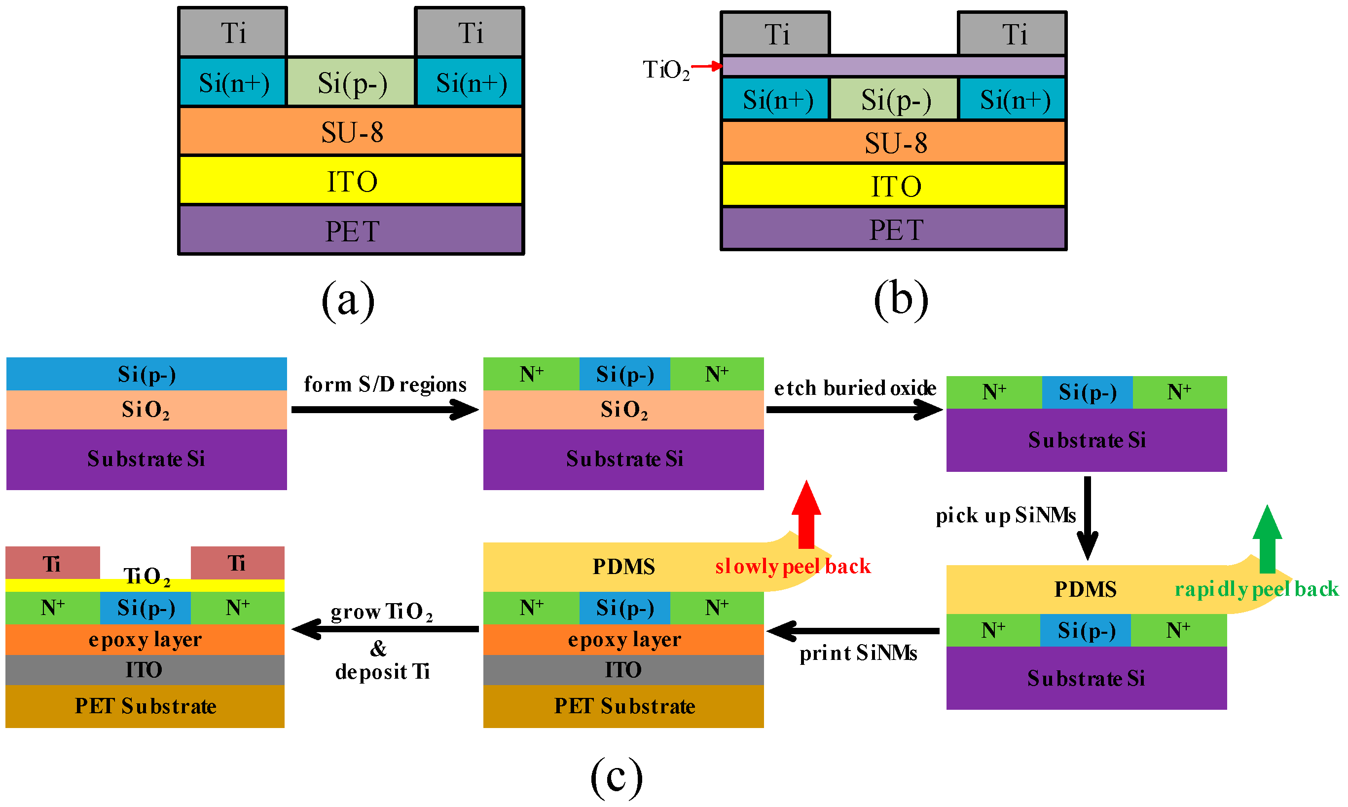
Abstract
1. Introduction
2. Materials and Methods
2.1. Device Fabrication
2.2. Device Characterization
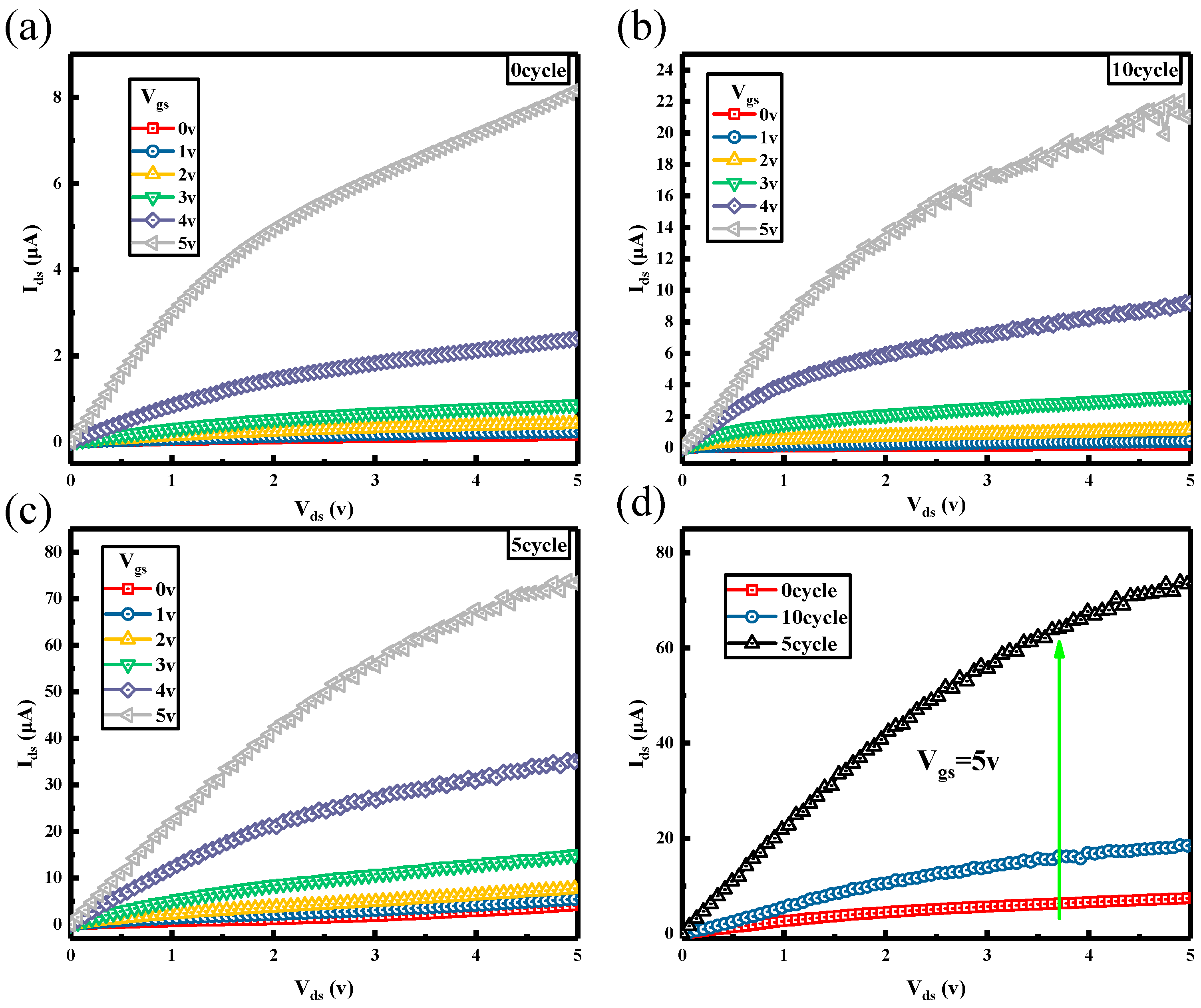
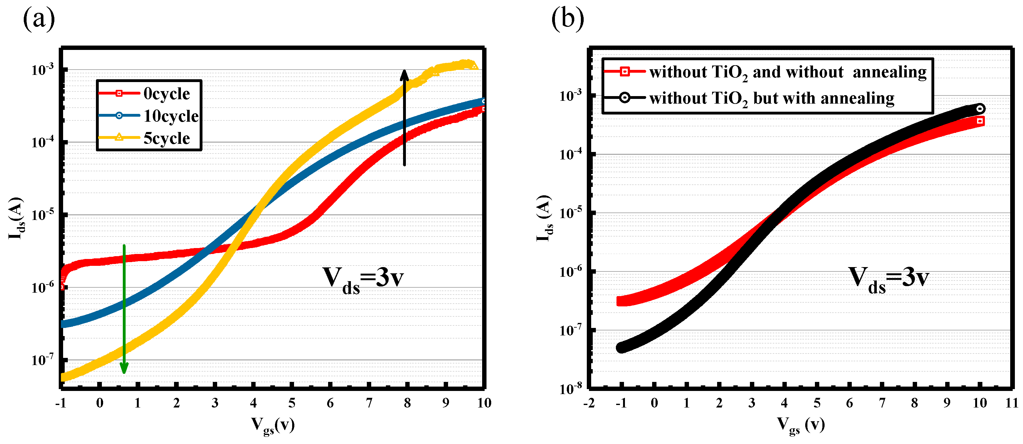
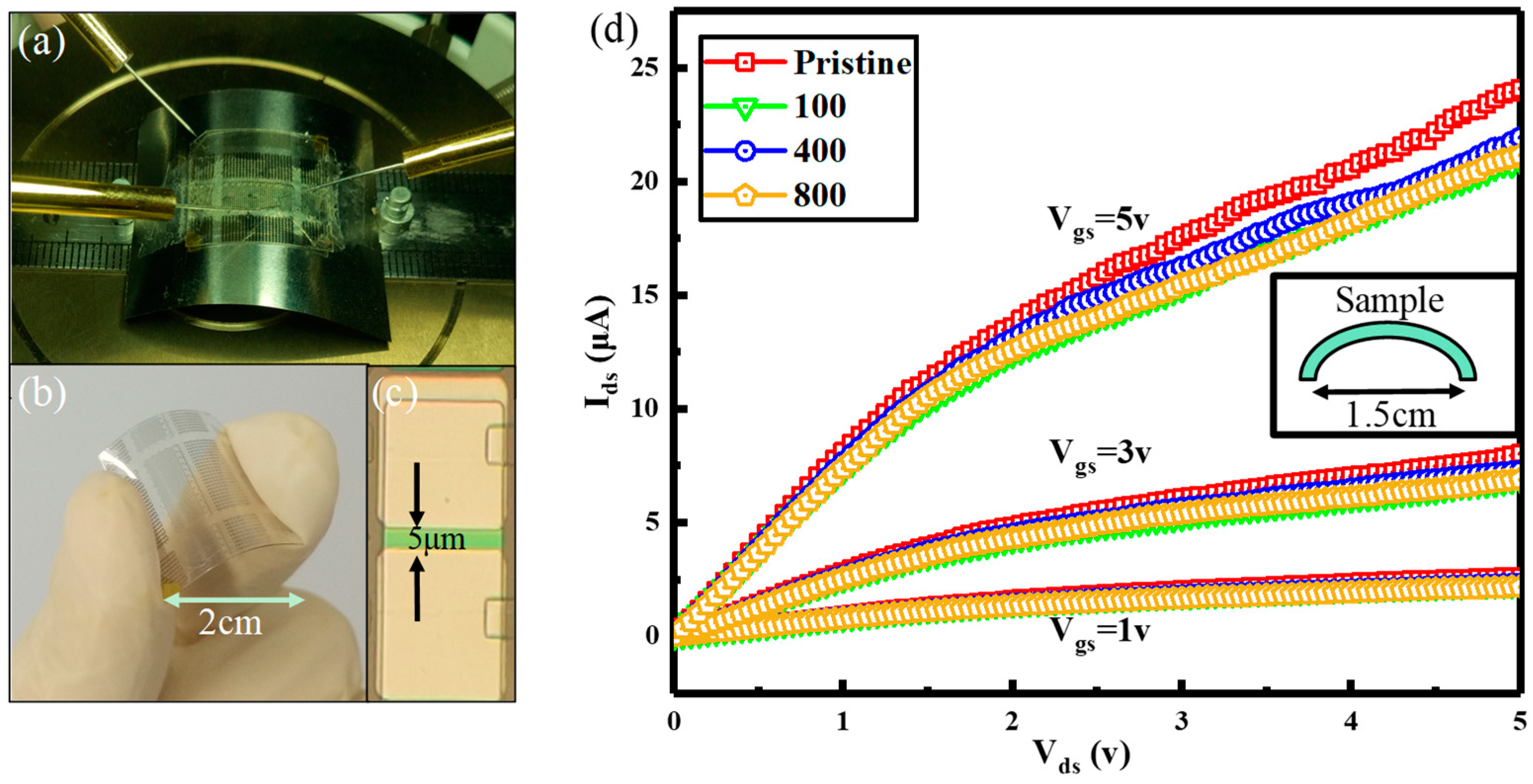
3. Results and Discussion
4. Conclusions
Author Contributions
Funding
Conflicts of Interest
References
- Kim, J.; Lee, M.; Shim, H.J.; Ghaffari, R.; Cho, H.R.; Son, D.; Jung, Y.H.; Soh, M.; Choi, C.; Jung, S.; et al. Stretchable silicon nanoribbon electronics for skin prosthesis. Nat. Commun. 2014, 5, 1–11. [Google Scholar] [CrossRef] [PubMed]
- Ying, M.; Bonifas, A.P.; Lu, N.; Su, Y.; Li, R.; Cheng, H.; Ameen, A.; Huang, Y.; Rogers, J.A. Silicon nanomembranes for fingertip electronics. Nanotechnology 2012, 23, 344004. [Google Scholar] [CrossRef] [PubMed]
- Park, M.; Kim, M.S.; Park, Y.K.; Ahn, J.H. Si membrane based tactile sensor with active matrix circuitry for artificial skin applications. Appl. Phys. Lett. 2015, 106, 043502. [Google Scholar] [CrossRef]
- Won, S.M.; Kim, H.S.; Lu, N.; Kim, D.G.; Del Solar, C.; Duenas, T.; Ameen, A.; Rogers, J.A. Piezoresistive strain sensors and multiplexed arrays using assemblies of single-crystalline silicon nanoribbons on plastic substrates. IEEE Trans. Electron Devices 2011, 58, 4074–4078. [Google Scholar] [CrossRef]
- Ahn, J.H.; Kim, H.S.; Lee, K.J.; Jeon, S.; Kang, S.J.; Sun, Y.; Nuzzo, R.G.; Rogers, J.A. Heterogeneous three-dimensional electronics by use of printed semiconductor nanomaterials. Science 2006, 314, 1754–1757. [Google Scholar] [CrossRef] [PubMed]
- Yang, S.; Lu, N. Gauge factor and stretchability of silicon-on-polymer strain gauges. Sensors 2013, 13, 8577–8594. [Google Scholar] [CrossRef]
- Lu, N.; Kim, D.-H. Flexible and Stretchable Electronics Paving the Way for Soft Robotics. Soft Robot. 2014, 1, 53–62. [Google Scholar] [CrossRef]
- Kim, D.H.; Ahn, J.H.; Kim, H.S.; Lee, K.J.; Kim, T.H.; Yu, C.J.; Nuzzo, R.G.; Rogers, J.A. Complementary logic gates and ring oscillators on plastic substrates by use of printed ribbons of single-crystalline silicon. IEEE Electron Device Lett. 2008, 29, 73–76. [Google Scholar] [CrossRef]
- Ahn, J.H.; Kim, H.S.; Menard, E.; Lee, K.J.; Zhu, Z.; Kim, D.H.; Nuzzo, R.G.; Rogers, J.A.; Amlani, I.; Kushner, V.; et al. Bendable integrated circuits on plastic substrates by use of printed ribbons of single-crystalline silicon. Appl. Phys. Lett. 2007, 90, 2005–2008. [Google Scholar] [CrossRef]
- Sun, L.; Qin, G.; Seo, J.H.; Celler, G.K.; Zhou, W.; Ma, Z. 12-GHz thin-film transistors on transferrable silicon nanomembranes for high-performance flexible electronics. Small 2010, 6, 2553–2557. [Google Scholar] [CrossRef]
- Yuan, H.C.; Celler, G.K.; Ma, Z. 7.8-GHz flexible thin-film transistors on a low-temperature plastic substrate. J. Appl. Phys. 2007, 102, 034501. [Google Scholar] [CrossRef]
- Torres Sevilla, G.A.; Almuslem, A.S.; Gumus, A.; Hussain, A.M.; Cruz, M.E.; Hussain, M.M. High performance high-κ/metal gate complementary metal oxide semiconductor circuit element on flexible silicon. Appl. Phys. Lett. 2016, 108, 094102. [Google Scholar] [CrossRef]
- Gupta, S.; Navaraj, W.T.; Lorenzelli, L.; Dahiya, R. Ultra-thin chips for high-performance flexible electronics. npj Flex. Electron. 2018, 2, 8. [Google Scholar] [CrossRef]
- Zhang, K.; Seo, J.H.; Zhou, W.; Ma, Z. Fast flexible electronics using transferrable silicon nanomembranes. J. Physics D Appl. Phys. 2012, 45, 143001. [Google Scholar] [CrossRef]
- Cohen, G.M.; Mooney, P.M.; Paruchuri, V.K.; Hovel, H.J. Dislocation-free strained silicon-on-silicon by in-place bonding. Appl. Phys. Lett. 2005, 86, 251902. [Google Scholar] [CrossRef]
- Song, E.; Guo, Q.; Huang, G.; Jia, B.; Mei, Y. Bendable Photodetector on Fibers Wrapped with Flexible Ultrathin Single Crystalline Silicon Nanomembranes. ACS Appl. Mater. Interfaces 2017, 9, 12171–12175. [Google Scholar] [CrossRef]
- Guo, Q.; Fang, Y.; Zhang, M.; Huang, G.; Chu, P.K.; Mei, Y.; Di, Z.; Wang, X. Wrinkled Single-Crystalline Germanium Nanomembranes for Stretchable Photodetectors. IEEE Trans. Electron Devices 2017, 64, 1985–1990. [Google Scholar] [CrossRef]
- Roberts, M.M.; Klein, L.J.; Savage, D.E.; Slinker, K.A.; Friesen, M.; Celler, G.; Eriksson, M.A.; Lagally, M.G. Elastically relaxed free-standing strained-silicon nanomembranes. Nat. Mater. 2006, 5, 388–393. [Google Scholar] [CrossRef]
- Song, E.; Fang, H.; Jin, X.; Zhao, J.; Jiang, C.; Yu, K.J.; Zhong, Y.; Xu, D.; Li, J.; Fang, G.; et al. Thin, Transferred Layers of Silicon Dioxide and Silicon Nitride as Water and Ion Barriers for Implantable Flexible Electronic Systems. Adv. Electron. Mater. 2017, 3, 1700077. [Google Scholar] [CrossRef]
- Meitl, M.A.; Zhu, Z.T.; Kumar, V.; Lee, K.J.; Feng, X.; Huang, Y.Y.; Adesida, I.; Nuzzo, R.G.; Rogers, J.A. Transfer printing by kinetic control of adhesion to an elastomeric stamp. Nat. Mater. 2006, 5, 33–38. [Google Scholar] [CrossRef]
- Carlson, A.; Bowen, A.M.; Huang, Y.; Nuzzo, R.G.; Rogers, J.A. Transfer printing techniques for materials assembly and micro/nanodevice fabrication. Adv. Mater. 2012, 24, 5284–5318. [Google Scholar] [CrossRef] [PubMed]
- Menard, E.; Lee, K.J.; Khang, D.Y.; Nuzzo, R.G.; Rogers, J.A. A printable form of silicon for high performance thin film transistors on plastic substrates. Appl. Phys. Lett. 2004, 84, 5398–5400. [Google Scholar] [CrossRef]
- Stefanov, P.; Shipochka, M.; Stefchev, P.; Raicheva, Z.; Lazarova, V.; Spassov, L. XPS characterization of TiO2 layers deposited on quartz plates. J. Phys. Conf. Ser. 2008, 100, 012039. [Google Scholar] [CrossRef]
- Zhang, Y.; Liu, Y.; Han, G.; Liu, H.; Hao, Y. Improving metal/n-Ge ohmic contact by inserting TiO2 deposited by PEALD. Micro Nano Lett. 2018, 13, 801–803. [Google Scholar] [CrossRef]
- Hobbs, C.; Fonseca, L.; Dhandapani, V.; Samavedam, S.; Taylor, B.; Grant, J.; Dip, L.; Triyoso, D.; Hegde, R.; Gilmer, D.; et al. Fermi level pinning at the polySi/metal oxide interface. In Proceedings of the 2003 Symposium on VLSI Technology. Digest of Technical Papers (IEEE Cat. No.03CH37407), Kyoto, Japan, 10–12 June 2003; pp. 3–4. [Google Scholar] [CrossRef]
- Rim, Y.S.; Yang, Y.; Bae, S.H.; Chen, H.; Li, C.; Goorsky, M.S.; Yang, Y. Ultrahigh and Broad Spectral Photodetectivity of an Organic-Inorganic Hybrid Phototransistor for Flexible Electronics. Adv. Mater. 2015, 27, 6885–6891. [Google Scholar] [CrossRef] [PubMed]


© 2018 by the authors. Licensee MDPI, Basel, Switzerland. This article is an open access article distributed under the terms and conditions of the Creative Commons Attribution (CC BY) license (http://creativecommons.org/licenses/by/4.0/).
Share and Cite
Zhang, J.; Zhang, Y.; Chen, D.; Zhu, W.; Xi, H.; Zhang, J.; Zhang, C.; Hao, Y. Bendable Single Crystal Silicon Nanomembrane Thin Film Transistors with Improved Low-Temperature Processed Metal/n-Si Ohmic Contact by Inserting TiO2 Interlayer. Nanomaterials 2018, 8, 1060. https://doi.org/10.3390/nano8121060
Zhang J, Zhang Y, Chen D, Zhu W, Xi H, Zhang J, Zhang C, Hao Y. Bendable Single Crystal Silicon Nanomembrane Thin Film Transistors with Improved Low-Temperature Processed Metal/n-Si Ohmic Contact by Inserting TiO2 Interlayer. Nanomaterials. 2018; 8(12):1060. https://doi.org/10.3390/nano8121060
Chicago/Turabian StyleZhang, Jiaqi, Yi Zhang, Dazheng Chen, Weidong Zhu, He Xi, Jincheng Zhang, Chunfu Zhang, and Yue Hao. 2018. "Bendable Single Crystal Silicon Nanomembrane Thin Film Transistors with Improved Low-Temperature Processed Metal/n-Si Ohmic Contact by Inserting TiO2 Interlayer" Nanomaterials 8, no. 12: 1060. https://doi.org/10.3390/nano8121060
APA StyleZhang, J., Zhang, Y., Chen, D., Zhu, W., Xi, H., Zhang, J., Zhang, C., & Hao, Y. (2018). Bendable Single Crystal Silicon Nanomembrane Thin Film Transistors with Improved Low-Temperature Processed Metal/n-Si Ohmic Contact by Inserting TiO2 Interlayer. Nanomaterials, 8(12), 1060. https://doi.org/10.3390/nano8121060