Article

Fabrication of Si/graphene/Si Double Heterostructures by Semiconductor Wafer Bonding towards Future Applications in Optoelectronics

Department of Chemical Engineering, Kyoto University, Kyoto 615-8510, Japan
*
Author to whom correspondence should be addressed.
Nanomaterials 2018, 8(12), 1048; https://doi.org/10.3390/nano8121048
Submission received: 11 November 2018 / Revised: 4 December 2018 / Accepted: 12 December 2018 / Published: 14 December 2018
(This article belongs to the Special Issue Nanotechnologies and Nanomaterials: Selected Papers from CCMR 2019)

Abstract

:
A Si/graphene/Si planar double heterostructure has been fabricated by means of semiconductor wafer bonding. The interfacial mechanical stability and interlayer electrical connection have been verified for the structure. To the best of our knowledge, this is the first realization of a monolayer-cored double heterostructure. In addition, a double heterostructure with bilayer graphene has been prepared for bandgap generation and tuning by application of a bias voltage. These structures move towards the realization of versatile graphene optoelectronics, such as an electrically pumped graphene laser. Our Si/graphene/Si double heterostructure is positioned to form a new basis for next-generation nanophotonic devices with high photon and carrier confinements, earth abundance (C, Si), environmental safety (C, Si), and excellent optical and electrical controllability by silicon clads.

1. Introduction

Monolayer-material-based optoelectronic devices possess promising characteristics for high-density integration, low-power-consumption, and high-speed operation [1,2,3,4,5,6,7,8,9,10,11]. However, monolayer materials have been used nakedly in the devices reported so far, and such devices suffer from a substantial amount of electrical and optical losses. To address this issue, we have employed monolayer-cored double heterostructures [12,13], which allow for carrier and photon confinements. Monolayer-gained semiconductor lasers show promise in the nanophotonics field [14,15]. Graphene lasers, if realized, would be an ultimate component in optoelectronics in view of environmental friendliness, potential low cost, small scale for high-density integration, and superb physical properties [3,7,9]. Semiconductor wafer bonding [16,17,18,19,20,21,22] is utilized to form heterostructures of dissimilar semiconductor materials with low defect densities, which is otherwise difficult to obtain by the conventional growth method due to the crystalline lattice mismatch. Wafer bonding is therefore promising for fabrication of high-performance semiconductor optoelectronics, and has been employed to generate a variety of heterostructured devices [23,24,25,26,27,28,29]. Here, we have fabricated a Si/graphene/Si double heterostructure by graphene-mediated bonding, serving as the first preparation of a monolayer-cored double heterostructure capable of providing a future basis for high-performance nanophotonic devices.

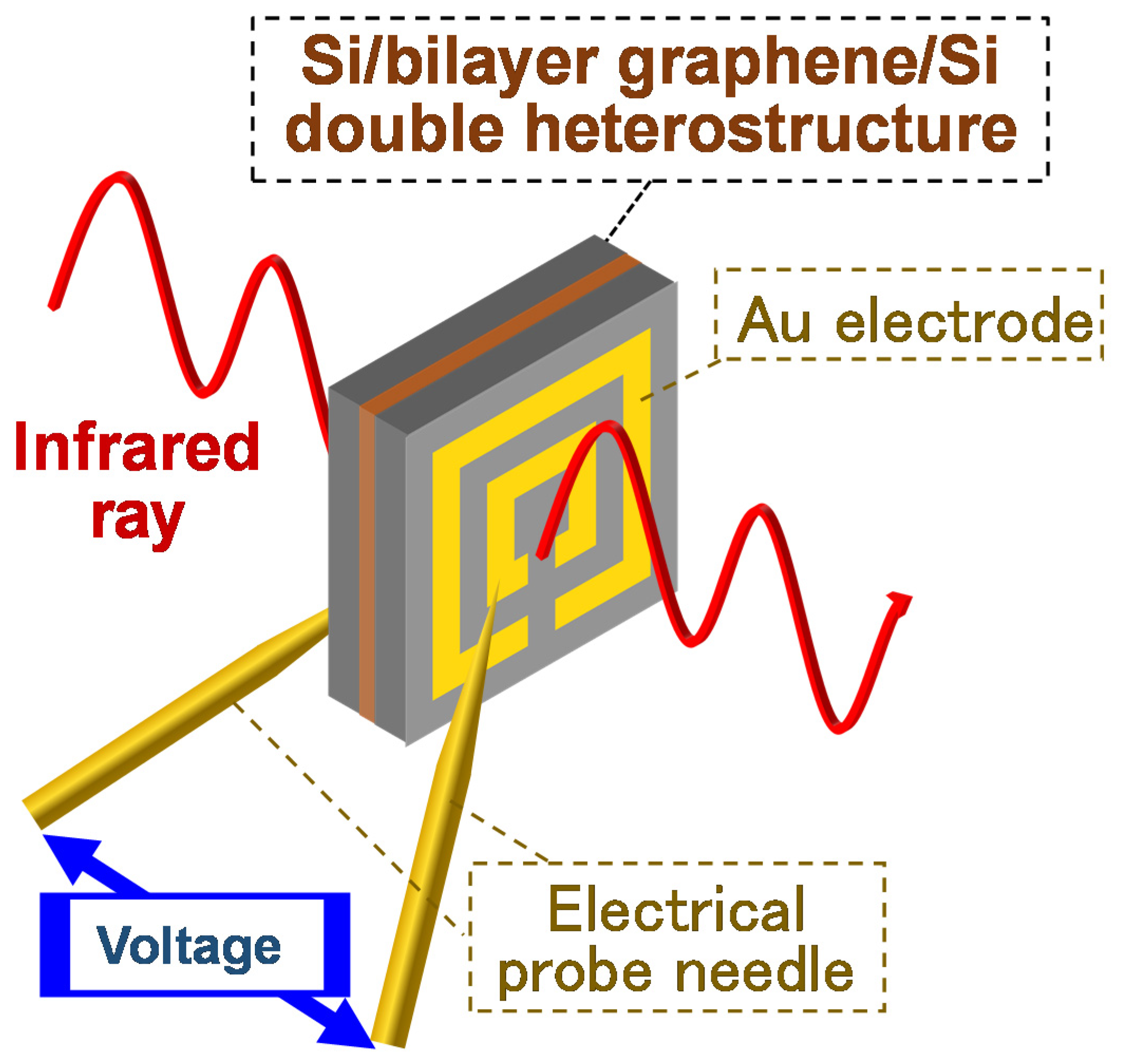
2. Experimental Methods

We used commercially available monolayer and bilayer graphene materials (Graphene Platform Corporation, Yokohama, Japan) in this work. Silicon, a versatile semiconductor, was adopted as the cladding material. We used single-side polished, epi-ready p-type Si <100> wafers doped with boron (doping concentration of ~1 × 1019 cm−3) and double-side polished, epi-ready p-type Si <100> wafers doped with boron (doping concentration of ~1 × 1016 cm−3). Large-area graphene sheets (~20 cm2) transferred onto the polished-side surface of the Si wafers was used in this study. In an attempt to create balance between ease in obtaining electric measurements from ohmic metal contacts and optical transparency for transmission measurements, the higher and lower doping-concentration Si wafers were used for monolayer and bilayer graphene, respectively. The Si wafer topped with a graphene layer was cut into ~1 cm2 area dies after being coated with a photoresist, in order to protect the bonding surface from particles generated during the cutting process. During cutting, no issues were observed for the graphene layer, which remained intact on the Si wafer and did not experience delamination. A bare Si wafer was also coated with a photoresist and then cut into ~0.64 cm2 area dies. Immediately before bonding, the photoresist on both dies was removed with acetone, along with degreasing of the bonding surfaces. The graphene-side surface of the graphene-on-Si wafer was brought into contact with the polished-side surface of a bare Si wafer with the same doping concentration, with their Si (011) edges aligned. The two die pieces were then bonded by annealing in ambient air for 3 h under a uniaxial pressure of 0.1 MPaG [28]. The detachment normal stresses were measured as the bonded interfacial strengths for the fabricated Si/graphene/Si samples, as well as Si/Si direct-bonded controls (no graphene). For current injection during electrical measurements, Al layers with a thickness of 100 nm were deposited by electron-beam evaporation as ohmic electrodes on both outer Si surfaces of the bonded samples containing a higher doping concentration. Alternatively, metal electrodes comprising an Au-Ge-Ni alloy (80:10:10 wt%) and pure Au with thicknesses of 30 and 150 nm, respectively, were sequentially deposited by thermal evaporation on the samples containing a lower doping concentration.
In the second part of this work, the functionality of the structure was demonstrated by attempting to generate and tune the graphene bandgap energy through application of an electrical bias voltage. Bilayer graphene [30] was used as the core material in the Si-cladded double heterostructure. Graphene bandgap energy is known to be detectable via observation of absorption peaks in transmission spectra [30]. According to Reference [30], bias voltages were applied in the normal direction of the planar Si/bilayer graphene/Si double heterostructures, and the measured optical transmission in the normal direction vertically penetrated the samples. Figure 1 depicts a conceptual drawing of the measurement system. Optical measurements utilizing Fourier-transform infrared spectroscopy (FTIR, PerkinElmer, Waltham, MA, USA) were conducted to observe the graphene bandgap. Attempts were made to detect the existence of the absorption peak induced by the bandgap energy, by eliminating optical interference from the acquired transmission spectral data using the after-mentioned theoretical calculations. Due to facility limitations, measurements were conducted in ambient air at room temperature in the photon energy range from 0.05 to 0.85 eV and applied bias voltage from −20 to 20 V. To clarify the change in transmission spectra induced by the bias voltage, the raw transmission spectra data obtained with bias voltage, V, were normalized to that without electrical bias (i.e., V = 0).

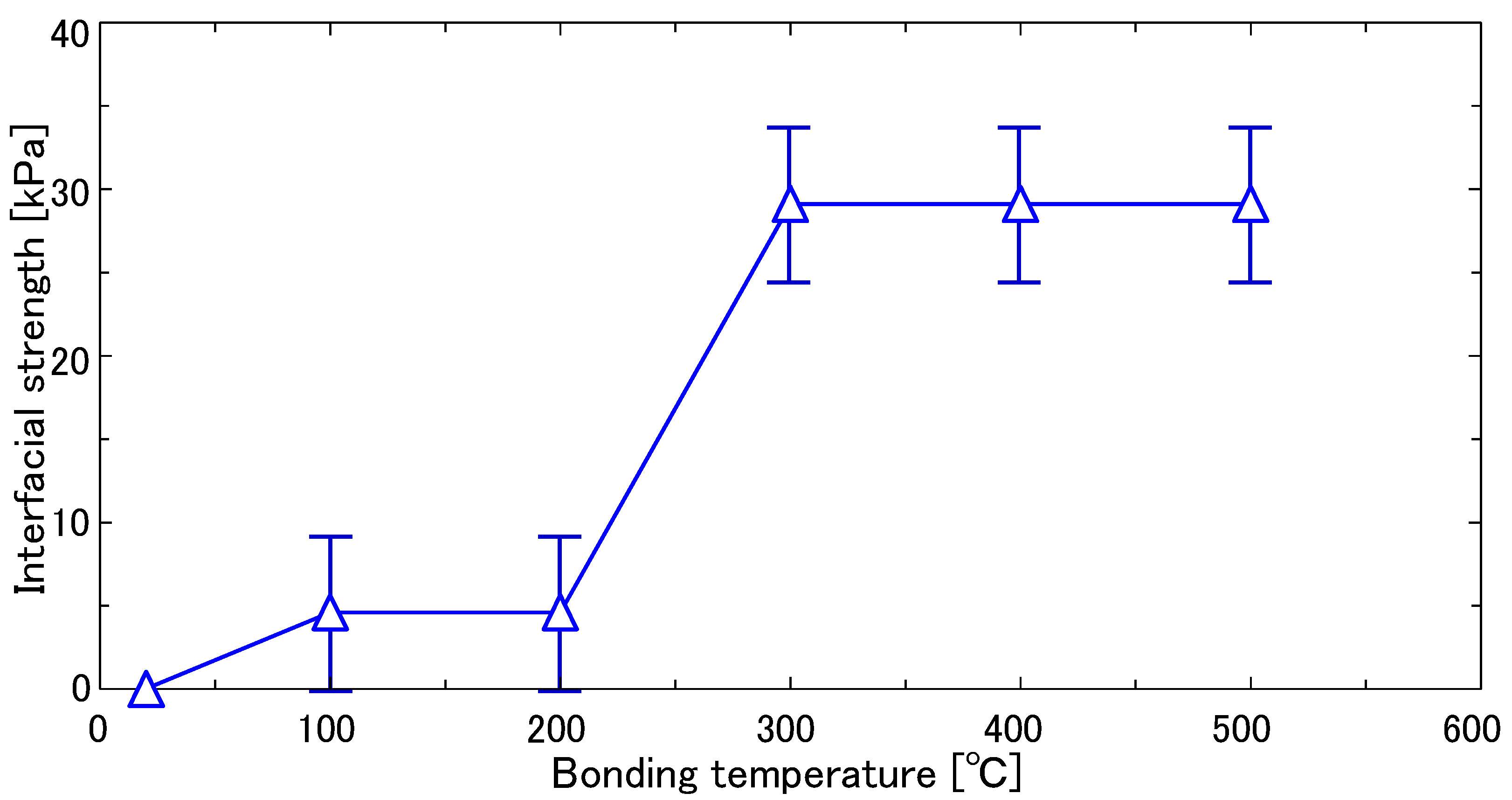
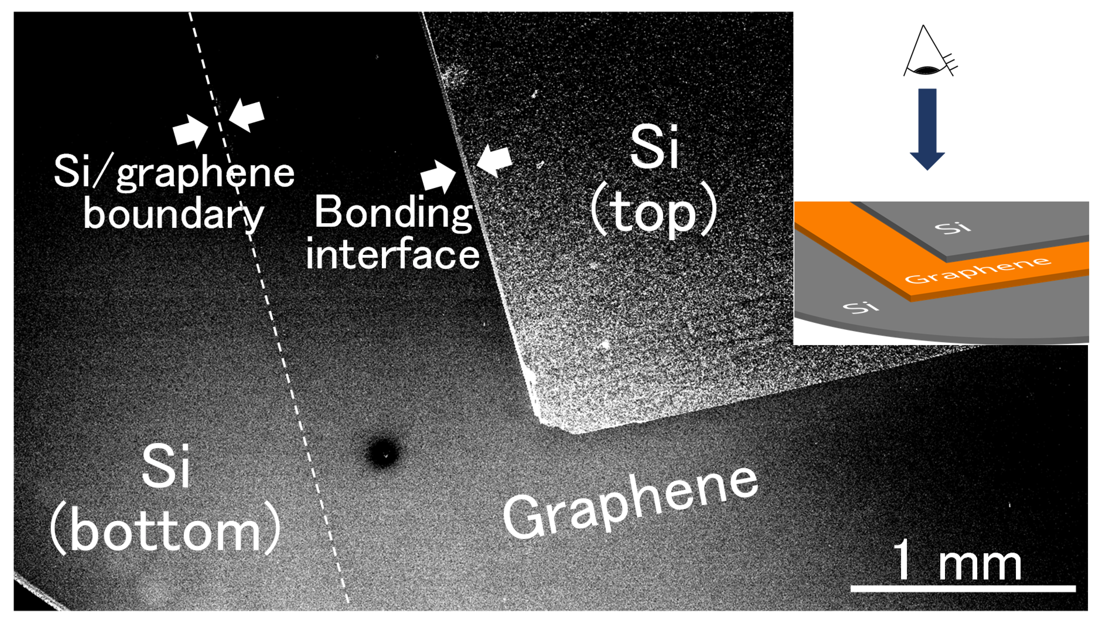
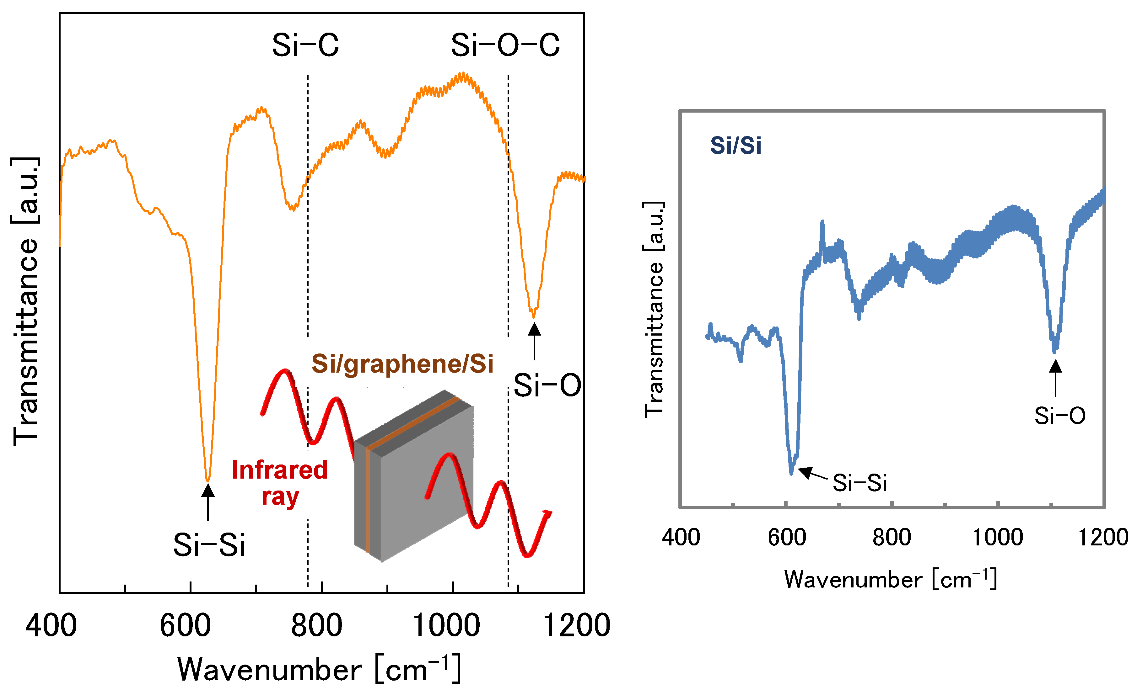
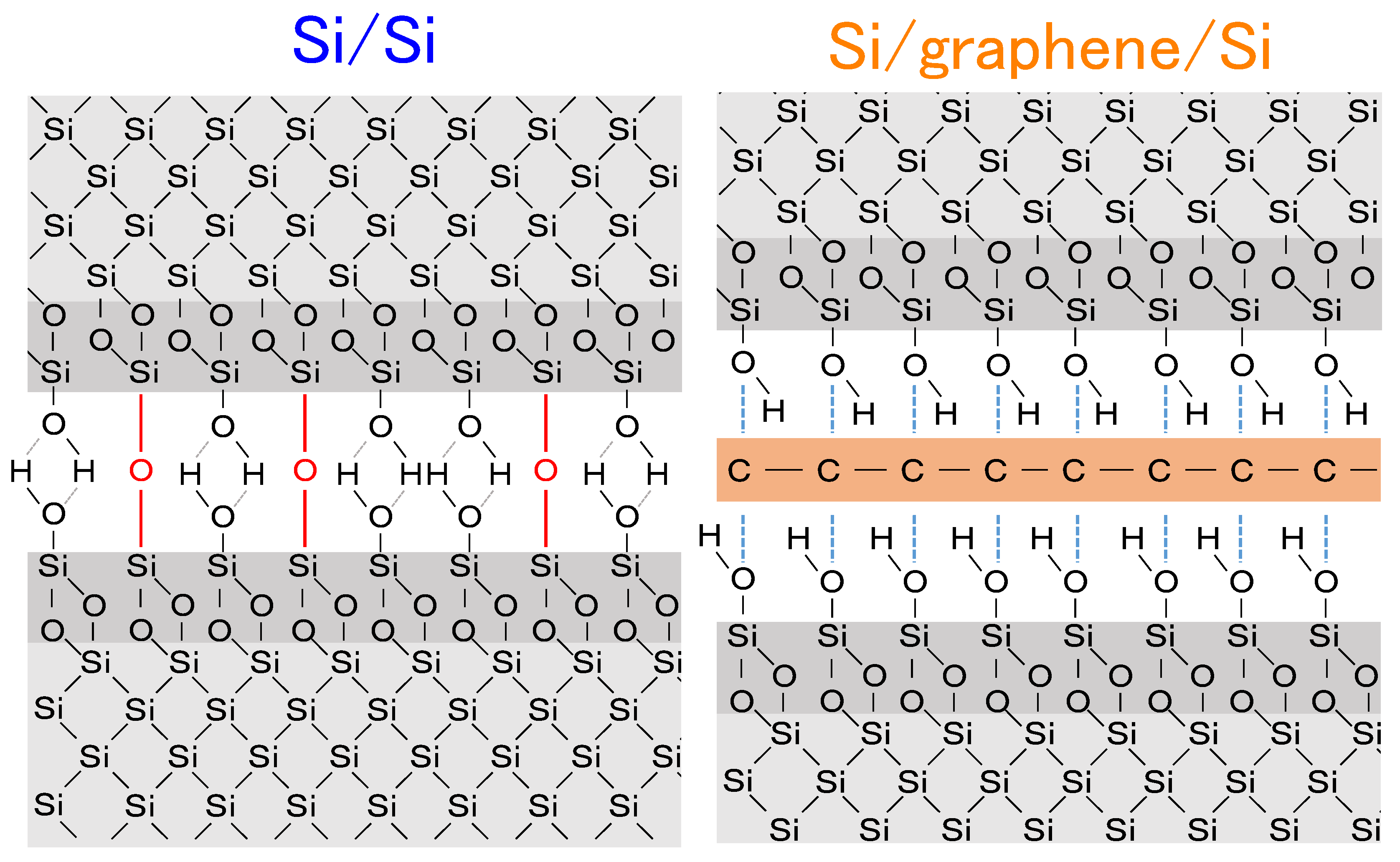
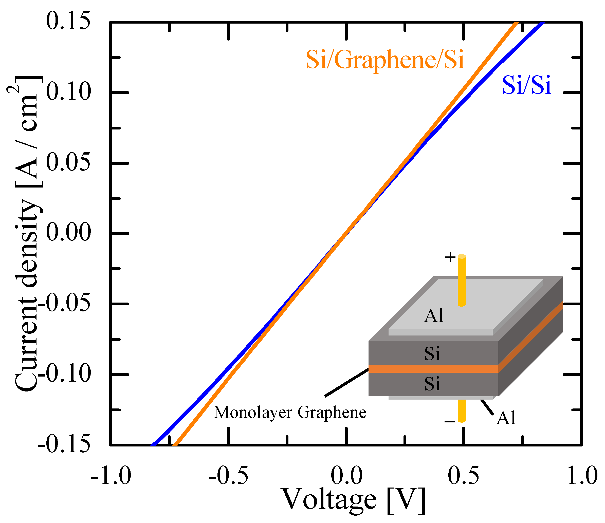
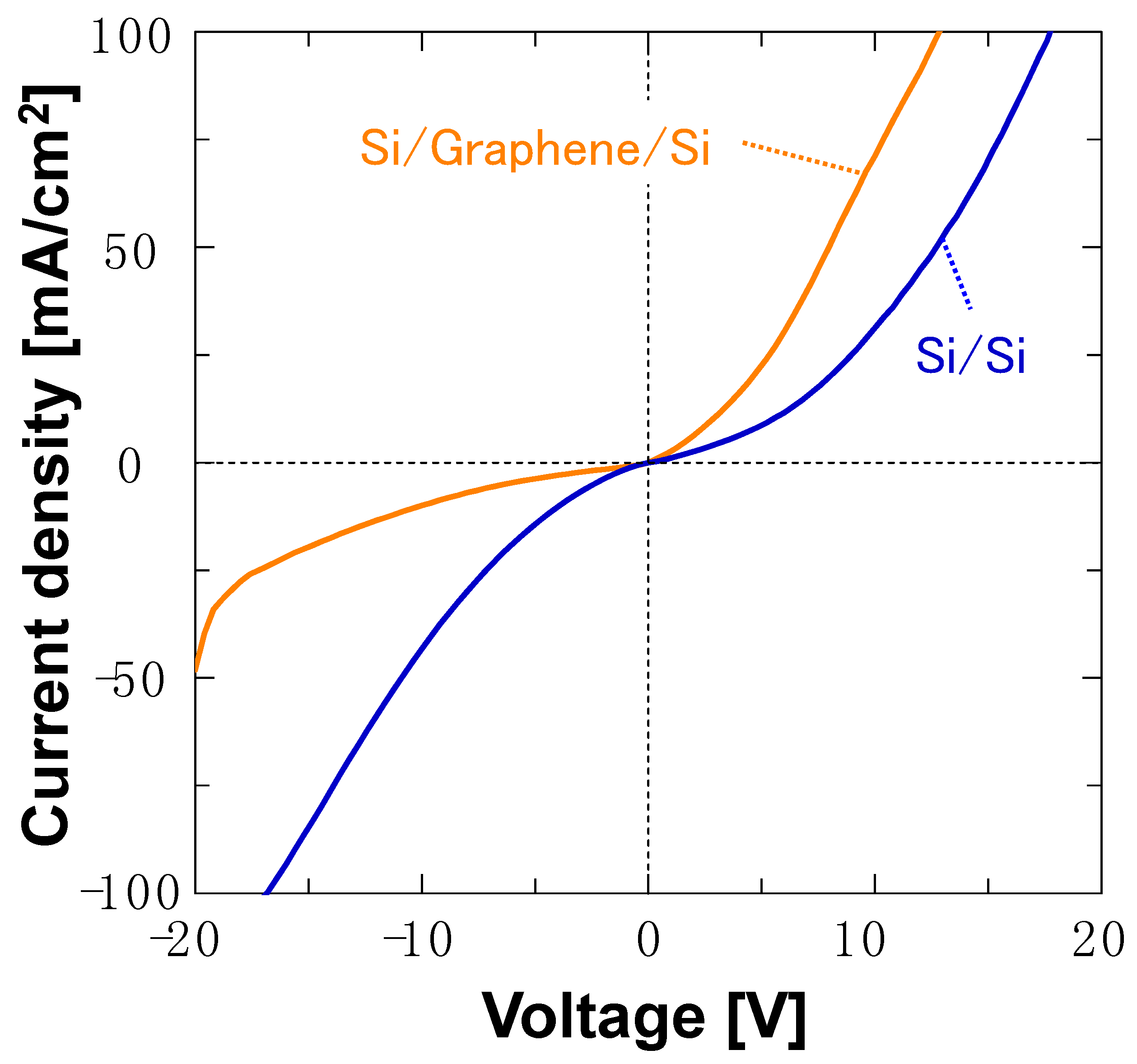
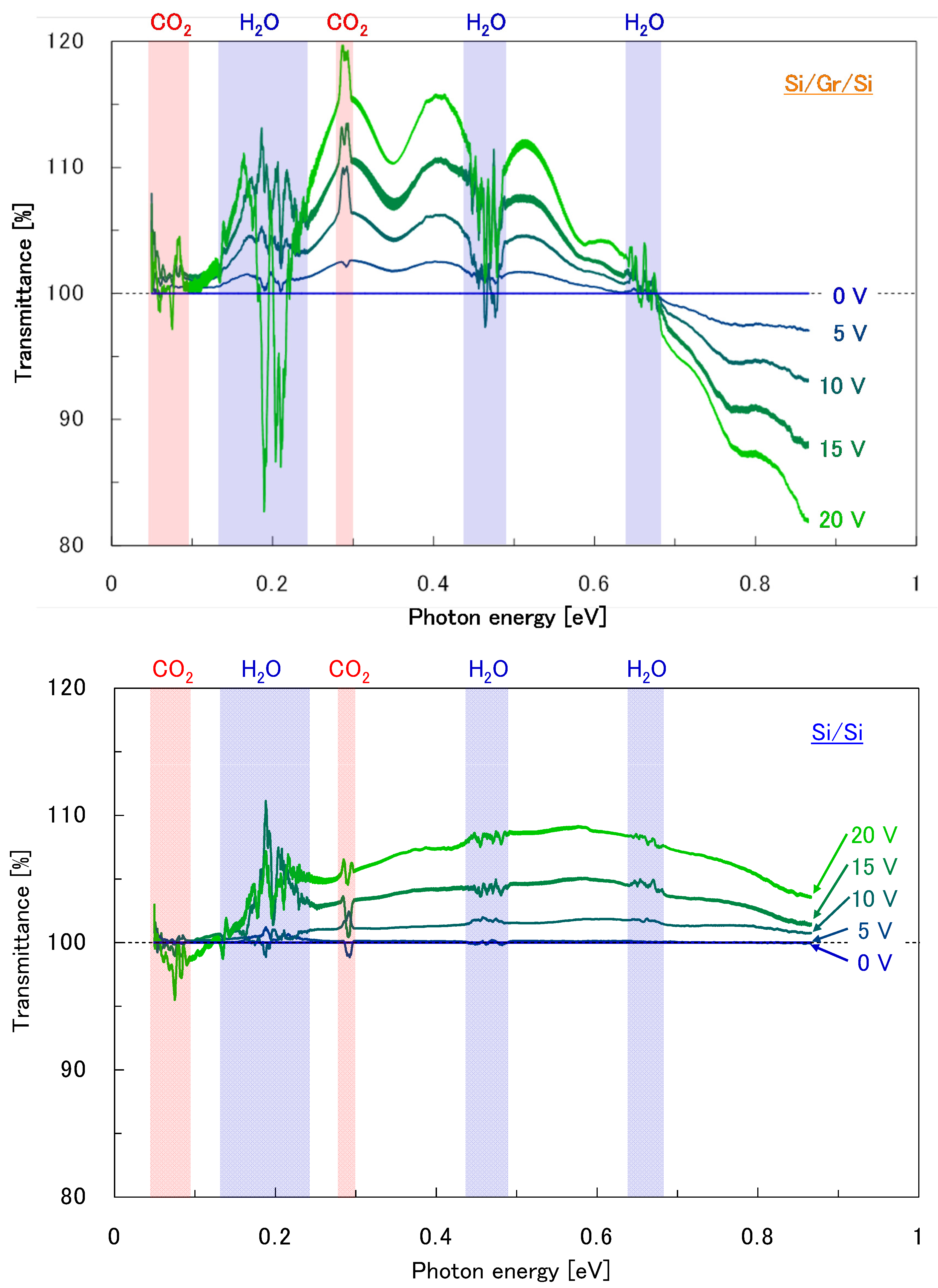
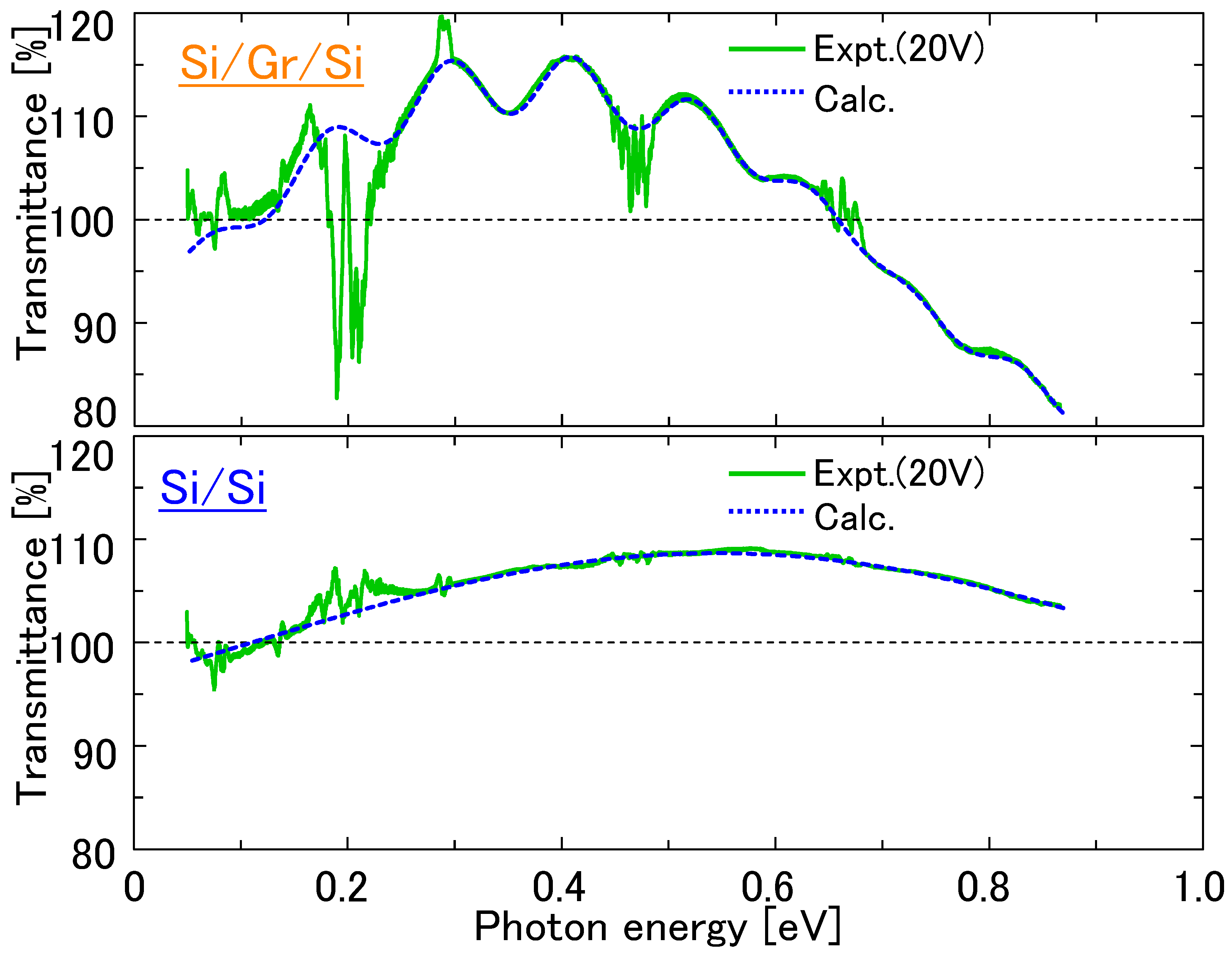
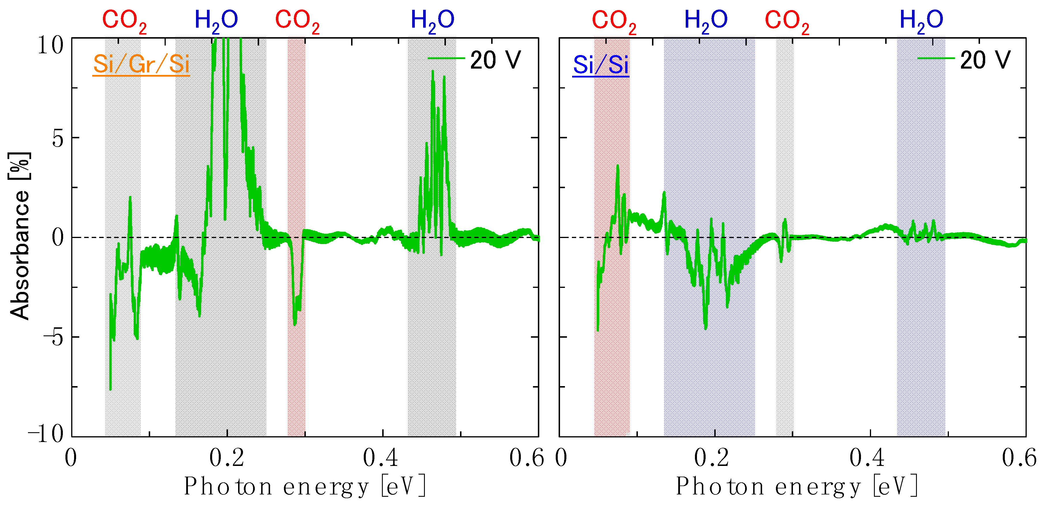
3. Results and Discussion

Interfacial bonding strength as a function of temperature was first analyzed, where the temperature varied from room temperature (20 °C) to 500 °C. Figure 2 shows the dependence of the interfacial bonding strength in the Si/monolayer graphene/Si structure on bonding temperature. For temperatures below 300 °C, an increase in the bonding strength with bonding temperature was observed. This can be attributed to diffusion of residual water on the bonding surfaces into the bulk Si region and/or outgassing from the bonded interface by vaporization. On the contrary, no significant increase in the bonding strength for bonding temperatures above 300 °C was observed, and as a result, the optimum bonding temperature was determined to be 300 °C. Figure 3 shows a plane-view scanning electron microscope image of the fabricated Si/graphene/Si double heterostructure. Here, we have demonstrated success in the preparation of a monolayer-cored double heterostructure composed of Si/graphene/Si.
The measured interfacial bonding strength of the Si/graphene/Si structure (~30 kPa) was drastically reduced when compared to the Si/Si control structure without graphene (~650 kPa). To investigate the origin of this interfacial strength difference, an FTIR measurement was conducted on the Si/graphene/Si double heterostructure containing bilayer graphene, as the Si wafer used for monolayer graphene was not transparent. Absorption peaks for covalent Si–C and Si–O–C bonds [31] were not observed in the measurement, as seen in Figure 4. Figure 5 depicts a conceptual schematic of a cross-sectional molecular view of the bonded interfaces. It is known that covalent oxygen bridges are partially formed at the directly bonded Si/Si interface, therefore enhancing the bonding strength [20,21]. Alternatively, when graphene is present, interfacial covalent bonds do not form and the primary bonding forces include van der Waals interactions and hydrogen bonds. These interfacial chemical bonding differences are hypothesized to be the cause for mechanical strength differences in the Si/graphene/Si structure relative to the Si/Si control.
Figure 6 and Figure 7 show the room-temperature current-voltage characteristics of the Si/monolayer graphene/Si and Si/bilayer graphene/Si double heterostructures, respectively, compared to the Si/Si control sample with the same doping-concentration Si wafer for each. The interfacial electrical resistivity across the Si/monolayer graphene/Si structure was less than 5 Ω cm2, and comparable to that for the corresponding Si/Si control, as seen in Figure 6. Thus, a favorable electrical interlayer conductance has been obtained in the bonded Si/graphene/Si double heterostructure. The Si/bilayer graphene/Si double heterostructure exhibited a diode-like, rectified current-voltage curve, similar to that of the corresponding Si/Si control, as shown in Figure 7. This result is consistent with the existing reports that graphene/Si interfaces have Schottky-contact characteristics (for Si with regular doping concentrations) [32,33]. It is hypothesized that the asymmetry in the current-voltage curve, seen in Figure 7, for the Si/bilayer graphene/Si structure may be due to property differences between the two graphene/Si interfaces included in the double heterostructure for our samples. It should be noted that the difference in the electrical characteristics between Figure 6 and Figure 7 may not be due to differences between monolayer and bilayer graphene, but simply due to the difference in doping concentrations in the Si wafers used for each sample. In other words, Si with heavy, degenerating doping concentrations, as seen in the Si wafer used for the Si/bilayer graphene/Si structures here, may form heterointerfaces of the ohmic-contact property with graphene due to its metallic characteristics.
Figure 8 shows the FTIR transmission spectra with applied electrical bias for the Si/bilayer graphene/Si double heterostructure as well as the Si/Si control sample. The regions highlighted in blue and red contain noise originating from ambient concentration changes in H2O and CO2, respectively. As the applied voltage increases, oscillatory changes in the transmittances were observed for both the Si/bilayer graphene/Si and reference Si/Si samples. This spectral oscillation can be attributed to the optical interference at the bonded interfaces, which are magnified due to the existence of interfacial voids. These interfacial voids are known to exist partially at bonded interfaces, originating from airborne particles or partial missing bonds [34,35,36,37], or potentially partial polymer residue used in the graphene transfer process by the vendor, and are presumably expanded by temperature increases induced by the applied electrical bias in the samples.
For clearer quantitative examination of the transmission spectra, the interference effect was eliminated from the data using a mathematical model for the interference mechanism, as shown below. The change in transmittance is formulated, accounting for the voids of various sizes as:
Δ T = k = 1 m A k sin { 2 π · 2 n h v o i d · 1 h c ( E p h o t o n Φ ) }
where Ak is the amplitude, n is refractive index, hvoid is the void height, h is the Planck constant, c is the speed of light, Ephoton is the photon energy, and Φ is the phase offset. Figure 9 shows the fitting result of Equation (1) to the FTIR transmission spectra for the Si/bilayer graphene/Si and Si/Si structures at the applied bias voltage of 20 V. By subtracting the optical interference effect, obtained as Figure 9, from the original transmission data in Figure 8, attempts were made to clarify the intrinsic absorption by graphene, which is shown in Figure 10. Comparing Figure 10 (left) and (right), there is no significant optical absorption seen in graphene below the level of the atmospheric noise. Thus, we have not been able to observe a signature for graphene bandgap opening, like that reported in Reference [30], for our measurement conditions and sample structure including: Configuration of the metal electrodes, applied bias amplitudes, spectral measurement energy range, and environmental noise level. However, we have presented an experimental scheme for bandgap detection in a planar double heterostructure.
Our fabrication of the Si/graphene/Si structure is the first realization of a monolayer-cored double heterostructure, to the best of our knowledge. Importantly, the choice and use of the chemical elements of carbon (C, graphene) and silicon (Si) presented here have been proven suitable for future device use due to their low cost, earth abundance, and environmental friendliness. The Si/graphene/Si double heterostructures presented here can form a new basis for the next-generation nanophotonic devices with superb optical and electrical properties provided by the graphene [3,7,9], and high photon, carrier confinements, and excellent optical and electrical controllability provided by silicon clads. We would like to stress that a great advantage of the wafer bonding technique is its capability to fabricate double heterostructures that are not formable by conventional growth methods. We hereby realized a monocrystalline Si/graphene/monocrystalline Si double heterostructure, unable to be constructed by epitaxy, by utilizing wafer bonding. Our fabrication scheme and structure provide a new device platform for high-efficiency nano-optoelectronics. The results presented here are the first realization/demonstration of semiconductor wafer bonding mediated by an atomic monolayer, to the best of our knowledge. There exists potential for alternate monolayer materials, including graphene, to also be suitable as mediating agents for semiconductor bonding in optoelectronic applications, such as multijunction solar cells, due to their high adhesion strength [38], thermal and electrical conductivity [3,7,9], optical transparency [39], and environmental friendliness. Incorporation of a Si etch-back [40,41] or ion-cutting [42,43,44] technique, or the use of commercial silicon-on-insulator wafers [19,45,46] with HF separation, would enable the production of thin-film devices comprising Si/graphene/Si double heterostructures for lightweight, flexible, and ambient optoelectronics [47,48,49,50,51] composed of environmentally and human-body friendly chemical elements (C, Si).

4. Conclusions

In this work, we have fabricated, for the first time, a monolayer-cored double heterostructure, towards the realization of high-efficiency nano-optoelectronic devices. We prepared a Si/graphene/Si stack by means of graphene-mediated wafer bonding and verified the interfacial mechanical stability and interlayer electrical connection, demonstrating a new application of wafer bonding. The fabrication scheme and structure presented here provides a new device platform for functional monolayer materials.

Author Contributions

K.T. conceived the idea and designed the experiments. K.T. set up the wafer bonding facility and carried out the initial bonding tests. T.N. fabricated the samples, performed the measurements and calculations, and analyzed the data. Both authors contributed to discussion of the results and composed the manuscript.

Funding

This research was funded by the Inamori Foundation, Shorai Foundation for Science and Technology, Tonen General Foundation, and Japan Society for the Promotion of Science.

Acknowledgments

The authors would like to thank Yuta Hikima of Kyoto University for his support on the FTIR measurements, and Noriaki Sano of Kyoto University, Satoru Masubuchi and Yuan-Hsuan Jhang of the University of Tokyo for discussions.

Conflicts of Interest

The authors declare no conflict of interest. The funders had no role in the design of the study; in the collection, analyses, or interpretation of data; in the writing of the manuscript, or in the decision to publish the results.

References

  1. Novoselov, K.S.; Geim, A.K.; Morozov, S.V.; Jiang, D.; Zhang, Y.; Dubonos, S.V.; Grigorieva, I.V.; Firsov, A.A. Electric field effect in atomically thin carbon films. Science 2004, 306, 666–669. [Google Scholar] [CrossRef] [PubMed]
  2. Novoselov, K.S.; Jiang, D.; Schedin, F.; Booth, T.J.; Khotkevich, V.V.; Morozov, S.V.; Geim, A.K. Two-dimensional atomic crystals. Proc. Natl. Acad. Sci. USA 2005, 102, 10451–10453. [Google Scholar] [CrossRef] [Green Version]
  3. Geim, A.K.; Novoselov, K.S. The rise of graphene. Nat. Mater. 2007, 6, 183–191. [Google Scholar] [CrossRef] [PubMed]
  4. Xia, F.; Mueller, T.; Lin, Y.; Valdes-Garcia, A.; Avouris, P. Ultrafast graphene photodetector. Nat. Nanotechnol. 2009, 4, 839–843. [Google Scholar] [CrossRef] [PubMed] [Green Version]
  5. Mueller, T.; Xia, F.; Avouris, P. Graphene photodetectors for high-speed optical communications. Nat. Photon. 2010, 4, 297–301. [Google Scholar] [CrossRef] [Green Version]
  6. Liu, M.; Yin, X.B.; Ulin-Avila, E.; Geng, B.S.; Zentgraf, T.; Ju, L.; Wang, F.; Zhang, X. A graphene-based broadband optical modulator. Nature 2011, 474, 64–67. [Google Scholar] [CrossRef] [PubMed]
  7. Geim, A.K.; Grigorieva, I.V. Van der Waals heterostructures. Nature 2013, 499, 419–425. [Google Scholar] [CrossRef] [Green Version]
  8. Kim, Y.D.; Kim, H.; Cho, Y.; Ryoo, J.H.; Park, C.H.; Kim, P.; Kim, Y.S.; Lee, S.; Li, Y.L.; Park, S.N.; et al. Bright visible light emission from graphene. Nat. Nanotechnol. 2015, 10, 676–681. [Google Scholar] [CrossRef] [Green Version]
  9. Novoselov, K.S.; Mishchenko, A.; Carvalho, A.; Castro Neto, A.H. 2D materials and van der Waals heterostructures. Science 2016, 353, aac9439. [Google Scholar] [CrossRef]
  10. Negishi, R.; Akabori, M.; Ito, T.; Watanabe, Y.; Kobayashi, Y. Band-like transport in highly crystalline graphene films from defective graphene oxides. Sci. Rep. 2016, 6, 28936. [Google Scholar] [CrossRef] [Green Version]
  11. Masubuchi, S.; Morimoto, M.; Morikawa, S.; Onodera, M.; Asakawa, Y.; Watanabe, K.; Taniguchi, T.; Machida, T. Autonomous robotic searching and assembly of two-dimensional crystals to build van der Waals superlattices. Nat. Commun. 2018, 9, 1413. [Google Scholar] [CrossRef] [PubMed]
  12. Alferov, Z.I. Nobel lecture: The double heterostructure concept and its applications in physics, electronics, and technology. Rev. Mod. Phys. 2001, 73, 767–782. [Google Scholar] [CrossRef]
  13. Kroemer, H. Nobel lecture: Quasielectric fields and band offsets: Teaching electrons new tricks. Rev. Mod. Phys. 2001, 73, 783–793. [Google Scholar] [CrossRef]
  14. Wu, S.F.; Buckley, S.; Schaibley, J.R.; Feng, L.F.; Yan, J.Q.; Mandrus, D.G.; Hatami, F.; Yao, W.; Vuckovic, J.; Majumdar, A. Monolayer semiconductor nanocavity lasers with ultralow thresholds. Nature 2015, 520, 69–72. [Google Scholar] [CrossRef] [PubMed] [Green Version]
  15. Ye, Y.; Wong, Z.J.; Lu, X.; Ni, X.; Zhu, H.; Chen, X.; Wang, Y.; Zhang, X. Monolayer excitonic laser. Nat. Photon. 2015, 9, 733–737. [Google Scholar] [CrossRef] [Green Version]
  16. Nakamura, T. Method of Making a Semiconductor Device. U.S. Patent 3,239,908, 15 March 1966. [Google Scholar]
  17. Wallis, G.; Pomerantz, D.I. Field assisted glass-metal sealing. J. Appl. Phys. 1969, 40, 3946–3949. [Google Scholar] [CrossRef]
  18. Stern, F.; Woodall, J.M. Photon recycling in semiconductor lasers. J. Appl. Phys. 1974, 45, 3904–3906. [Google Scholar] [CrossRef]
  19. Lasky, J.B. Wafer bonding for silicon-on-insulator technologies. Appl. Phys. Lett. 1986, 48, 78–80. [Google Scholar] [CrossRef]
  20. Shimbo, M.; Furukawa, K.; Fukuda, K.; Tanzawa, K. Silicon-to-silicon direct bonding method. J. Appl. Phys. 1986, 60, 2987–2989. [Google Scholar] [CrossRef]
  21. Tong, Q.; Goesele, U.M. Wafer bonding and layer splitting for microsystems. Adv. Mater. 1999, 11, 1409–1425. [Google Scholar] [CrossRef]
  22. Moutanabbir, O.; Goesele, U. Heterogeneous integration of compound semiconductors. Ann. Rev. Mater. Res. 2010, 40, 469–500. [Google Scholar] [CrossRef]
  23. Wong, W.S.; Sands, T.; Cheung, N.W.; Kneissl, M.; Bour, D.P.; Mei, P.; Romano, L.T.; Johnson, N.M. InxGa1−xN light emitting diodes on Si substrates fabricated by Pd-In metal bonding and laser lift-off. Appl. Phys. Lett. 2000, 77, 2822–2824. [Google Scholar] [CrossRef]
  24. Noda, S.; Tomoda, K.; Yamamoto, N.; Chutinan, A. Full three-dimensional photonic bandgap crystals at near-infrared wavelengths. Science 2000, 289, 604–606. [Google Scholar] [CrossRef] [PubMed]
  25. Fang, A.W.; Park, H.; Cohen, O.; Jones, R.; Paniccia, M.J.; Bowers, J.E. Electrically pumped hybrid AlGaInAs-silicon evanescent laser. Opt. Express 2006, 14, 9203–9210. [Google Scholar] [CrossRef] [PubMed]
  26. Tanabe, K.; Fontcuberta i Morral, A.; Atwater, H.A.; Aiken, D.J.; Wanlass, M.W. Direct-bonded GaAs/InGaAs solar cell. Appl. Phys. Lett. 2006, 89, 102106. [Google Scholar] [CrossRef]
  27. Park, H.; Fang, A.W.; Jones, R.; Cohen, O.; Raday, O.; Sysak, M.N.; Paniccia, M.J.; Bowers, J.E. A hybrid AlGaInAs-silicon evanescent waveguide photodetector. Opt. Express 2007, 15, 6044–6052. [Google Scholar] [CrossRef] [PubMed]
  28. Tanabe, K.; Watanabe, K.; Arakawa, Y. III-V/Si hybrid photonic devices by direct fusion bonding. Sci. Rep. 2012, 2, 349. [Google Scholar] [CrossRef]
  29. Dimroth, F.; Grave, M.; Beutel, P.; Fiedeler, U.; Karcher, C.; Tibbits, T.N.D.; Oliva, E.; Siefer, G.; Schachtner, M.; Wekkeli, A. Wafer bonded four-junction GaInP/GaAs//GaInAsP/GaInAs concentrator solar cells with 44.7% efficiency. Prog. Photovolt. 2014, 22, 277–282. [Google Scholar] [CrossRef] [Green Version]
  30. Zhang, Y.B.; Tang, T.T.; Girit, C.; Hao, Z.; Martin, M.C.; Zettl, A.; Crommie, M.F.; Shen, Y.R.; Wang, F. Direct observation of a widely tunable bandgap in bilayer graphene. Nature 2009, 459, 820–823. [Google Scholar] [CrossRef]
  31. Ahmed, G.S.; Gilbert, M.; Mainprize, S.; Rogerson, M. FTIR analysis of silane grafted high density polyethylene. Plast. Rubber Compos. 2009, 38, 13–20. [Google Scholar] [CrossRef] [Green Version]
  32. Chen, C.C.; Aykol, M.; Chang, C.C.; Levi, A.F.J.; Cronin, S.B. Graphene-silicon Schottky diodes. Nano Lett. 2011, 11, 1863–1867. [Google Scholar] [CrossRef] [PubMed]
  33. Di Bartolomeo, A.; Luongo, G.; Iemmo, L.; Urban, F.; Giubileo, F. Graphene-silicon Schottky diodes for photodetection. IEEE Trans. Nanotechnol. 2018, 17, 1133–1137. [Google Scholar] [CrossRef]
  34. Esser, R.H.; Hobart, K.D.; Kub, F.J. Directional diffusion and void formation at a Si (001) bonded wafer interface. J. Appl. Phys. 2002, 92, 1945–1949. [Google Scholar] [CrossRef]
  35. Zhang, X.X.; Raskin, J.P. Low-temperature wafer bonding: A study of void formation and influence on bonding strength. J. Microelectromech. Syst. 2005, 14, 368–382. [Google Scholar] [CrossRef]
  36. Wang, C.X.; Higurashi, E.; Suga, T. Void-free room-temperature silicon wafer direct bonding using sequential plasma activation. Jpn. J. Appl. Phys. 2008, 47, 2526–2530. [Google Scholar] [CrossRef]
  37. Howlader, M.M.R.; Zhang, F. Void-free strong bonding of surface activated silicon wafers from room temperature to annealing at 600 degrees C. Thin Solid Films 2010, 519, 804–808. [Google Scholar] [CrossRef]
  38. Koenig, S.P.; Boddeti, N.G.; Dunn, M.L.; Bunch, J.S. Ultrastrong adhesion of graphene membranes. Nat. Nanotechnol. 2011, 6, 543–546. [Google Scholar] [CrossRef] [PubMed] [Green Version]
  39. Nair, R.R.; Blake, P.; Grigorenko, A.N.; Novoselov, K.S.; Booth, T.J.; Stauber, T.; Peres, N.M.R.; Geim, A.K. Fine structure constant defines visual transparency of graphene. Science 2008, 320, 1308. [Google Scholar] [CrossRef] [PubMed]
  40. Maszara, W.P.; Pronko, P.P.; McCormick, A.W. Epi-less bond-and-etch-back silicon-on-insulator by MeV ion-implantation. Appl. Phys. Lett. 1991, 58, 2779–2781. [Google Scholar] [CrossRef]
  41. Tong, Q.Y.; You, H.M.; Cha, G.; Goesele, U. Denuded zone formation in carbon-implanted silicon and its application to device quality silicon-on-insulator preparation. Appl. Phys. Lett. 1993, 62, 970–972. [Google Scholar] [CrossRef]
  42. Bruel, M. Silicon on insulator material technology. Electron. Lett. 1995, 31, 1201–1202. [Google Scholar] [CrossRef]
  43. Weldon, M.K.; Collot, M.; Chabal, Y.J.; Venezia, V.C.; Agarwal, A.; Haynes, T.E.; Eaglesham, D.J.; Christman, S.B.; Chaban, E.E. Mechanism of silicon exfoliation induced by hydrogen/helium co-implantation. Appl. Phys. Lett. 1998, 73, 3721–3723. [Google Scholar] [CrossRef]
  44. Hochbauer, T.; Misra, A.; Nastasi, M.; Mayer, J.W. Investigation of the cut location in hydrogen implantation induced silicon surface layer exfoliation. J. Appl. Phys. 2001, 89, 5980–5990. [Google Scholar] [CrossRef]
  45. Maszara, W.P.; Goetz, G.; Caviglia, A.; McKitterick, J.B. Bonding of silicon-wafers for silicon-on-insulator. J. Appl. Phys. 1988, 64, 4943–4950. [Google Scholar] [CrossRef]
  46. Celler, G.K.; Cristoloveanu, S. Frontiers of silicon-on-insulator. J. Appl. Phys. 2003, 93, 4955–4978. [Google Scholar] [CrossRef]
  47. Sekitani, T.; Nakajima, H.; Maeda, H.; Fukushima, T.; Aida, T.; Hata, K.; Someya, T. Stretchable active-matrix organic light-emitting diode display using printable elastic conductors. Nat. Mater. 2009, 8, 494–499. [Google Scholar] [CrossRef] [PubMed] [Green Version]
  48. Fan, Z.Y.; Razavi, H.; Do, J.W.; Moriwaki, A.; Ergen, O.; Chueh, Y.L.; Leu, P.W.; Ho, J.C.; Takahashi, T.; Reichertz, L.A.; et al. Three-dimensional nanopillar-array photovoltaics on low-cost and flexible substrates. Nat. Mater. 2009, 8, 648–653. [Google Scholar] [CrossRef] [PubMed]
  49. Tanabe, K.; Watanabe, K.; Arakawa, Y. Flexible thin-film InAs/GaAs quantum dot solar cells. Appl. Phys. Lett. 2012, 100, 192102. [Google Scholar] [CrossRef] [Green Version]
  50. Song, Y.M.; Xie, Y.Z.; Malyarchuk, V.; Xiao, J.L.; Jung, I.; Choi, K.J.; Liu, Z.J.; Park, H.; Lu, C.F.; Kim, R.H.; et al. Digital cameras with designs inspired by the arthropod eye. Nature 2013, 497, 95–99. [Google Scholar] [CrossRef] [PubMed]
  51. Nakata, S.; Shiomi, M.; Fujita, Y.; Arie, T.; Akita, S.; Takei, K. A wearable pH sensor with high sensitivity based on a flexible charge-coupled device. Nat. Electron. 2018, 1, 596–603. [Google Scholar] [CrossRef]
Figure 1. Conceptual drawing of the measurement system used for graphene bandgap tuning and detection.
Nanomaterials 08 01048 g001
Figure 2. Interfacial bonding strength as a function of temperature for the Si/graphene/Si structure.
Nanomaterials 08 01048 g002
Figure 3. Plane-view scanning electron microscope image of the fabricated Si/graphene/Si double heterostructure.
Nanomaterials 08 01048 g003
Figure 4. FTIR spectrum of (left) the Si/bilayer graphene/Si double heterostructure and (right) a Si/Si control structure.
Nanomaterials 08 01048 g004
Figure 5. Conceptual schematic of a cross-sectional molecular view of the bonded interfaces: (left) Si/Si control structure, (right) Si/graphene/Si double heterostructure.
Nanomaterials 08 01048 g005
Figure 6. Current-voltage characteristics of the Si/monolayer graphene/Si double heterostructure and corresponding Si/Si control structure with the same doping concentration (~1 × 1019 cm−3) in the Si wafer.
Nanomaterials 08 01048 g006
Figure 7. Current-voltage characteristics of the Si/bilayer graphene/Si double heterostructure and corresponding Si/Si control structure with the same doping concentration (~1 × 1016 cm−3) in the Si wafer.
Nanomaterials 08 01048 g007
Figure 8. FTIR transmission spectra with applied electrical bias for (top) the Si/bilayer graphene/Si double heterostructure and (bottom) the Si/Si control sample. The regions highlighted in blue and red contain noise originating from ambient concentration changes in H2O and CO2, respectively.
Nanomaterials 08 01048 g008
Figure 9. Comparison of the optical interference effect, represented in Equation (1), to the FTIR transmission spectra for (top) the Si/bilayer graphene/Si double heterostructure and (bottom) the Si/Si control structure at the applied bias voltage of 20 V.
Nanomaterials 08 01048 g009
Figure 10. Absorption spectra for (left) the Si/bilayer graphene/Si double heterostructure and (right) the Si/Si control sample at the applied bias voltage of 20 V, after elimination of the optical interference effect.
Nanomaterials 08 01048 g010

