Tailoring the Grain Size of Bi-Layer Graphene by Pulsed Laser Deposition

Abstract
1. Introduction
2. Experimental
3. Results and Discussion
4. Conclusions
Author Contributions
Funding
Conflicts of Interest
References
- Zhao, L.D.; Lo, S.H.; Zhang, Y.; Sun, H.; Tan, G.; Uher, C.; Wolverton, C.; Dravid, V.P.; Kanatzidis, M.G. Ultralow thermal conductivity and high thermoelectric figure of merit in SnSe crystals. Nature 2014, 508, 373–377. [Google Scholar] [CrossRef] [PubMed]
- Cavallaro, G.; Chiappisi, L.; Pasbakhsh, P.; Gradzielski, M.; Lazzara, G. A structural comparison of halloysite nanotubes of different origin by Small-Angle Neutron Scattering (SANS) and Electric Birefringence. Appl. Clay Sci. 2018, 160, 71–80. [Google Scholar] [CrossRef]
- Cavallaro, G.; Grillo, I.; Gradzielski, M.; Lazzara, G. Structure of hybrid materials based on halloysite nanotubes filled with anionic surfactants. J. Phys. Chem. C 2016, 120, 13492–13502. [Google Scholar] [CrossRef]
- Lazzara, G.; Cavallaro, G.; Panchal, A.; Fakhrullin, R.; Stavitskaya, A.; Vinokurov, V.; Lvov, Y. An assembly of organic-inorganic composites using halloysite clay nanotubes. Curr. Opin. Colloid Interface Sci. 2018, 35, 42–50. [Google Scholar] [CrossRef]
- Dragoman, D.; Dragoman, M. Giant thermoelectric effect in graphene. Appl. Phys. Lett. 2007, 91, 203116. [Google Scholar] [CrossRef]
- Xu, X.; Gabor, N.M.; Alden, J.S.; van der Zande, A.M.; McEuen, P.L. Photo-thermoelectric effect at a graphene interface junction. Nano Lett. 2009, 10, 562–566. [Google Scholar] [CrossRef] [PubMed]
- Kim, G.H.; Hwang, D.H.; Woo, S.I. Thermoelectric properties of nanocomposite thin films prepared with poly (3, 4-ethylenedioxythiophene) poly (styrenesulfonate) and graphene. Phys. Chem. Chem. Phys. 2012, 14, 3530–3536. [Google Scholar] [CrossRef] [PubMed]
- Shiau, L.L.; Wang, X.; Goh, S.C.K.; Chuan, K.; Ernst, H.; Tay, B.K. First demonstration of gate voltage-less chemical vapour deposition graphene for non-vacuum thermoelectric study. In Image Sensing Technologies: Materials, Devices, Systems, and Applications V. Int. Soc. Opt. Photonics 2018, 10656, 106561V. [Google Scholar]
- Ma, T.; Liu, Z.; Wen, J.X.; Gao, Y.; Ren, X.B.; Chen, H.J.; Jin, C.H.; Ma, X.L.; Xu, N.S.; Cheng, H.M.; et al. Tailoring the thermal and electrical transport properties of graphene films by grain size engineering. Nat. Commun. 2017, 8, 14486. [Google Scholar] [CrossRef] [PubMed]
- Yu, Q.; Lian, J.; Siriponglert, S.; Li, H.; Chen, Y.P.; Pei, S.S. Graphene segregated on Ni surfaces and transferred to insulators. Appl. Phys. Lett. 2008, 93, 113103. [Google Scholar] [CrossRef]
- Liu, W.; Li, H.; Xu, C.; Khatami, Y.; Banerjee, K. Synthesis of high-quality monolayer and bilayer graphene on copper using chemical vapor deposition. Carbon 2011, 49, 4122–4130. [Google Scholar] [CrossRef]
- Kim, K.S.; Zhao, Y.; Jang, H.; Lee, S.Y.; Kim, J.M.; Kim, K.S.; Ahn, J.H.; Kim, P.; Choi, J.Y.; Hong, B.H. Large-scale pattern growth of graphene films for stretchable transparent electrodes. Nature 2009, 457, 706–710. [Google Scholar] [CrossRef] [PubMed]
- Ago, H.; Ito, Y.; Mizuta, N.; Yoshida, K.; Hu, B.; Orofeo, C.M.; Tsuji, M.; Ikeda, K.; Mizuno, S. Epitaxial chemical vapor deposition growth of single-layer graphene over cobalt film crystallized on sapphire. ACS Nano 2010, 4, 7407–7414. [Google Scholar] [CrossRef] [PubMed]
- Perez, S.B.; Balbuena, P.B. Formation of Multilayer Graphene Domains with Strong Sulfur-Carbon Interaction and Enhanced Sulfur Reduction Zones for Lithium-Sulfur Battery Cathodes. ChemSusChem 2018, 11, 1970–1980. [Google Scholar] [CrossRef] [PubMed]
- Yazyev, O.V.; Chen, Y.P. Polycrystalline graphene and other two-dimensional materials. Nat. Nanotechnol. 2014, 9, 755–767. [Google Scholar] [CrossRef] [PubMed]
- Fei, Z.; Rodin, A.S.; Gannett, W.; Dai, S.; Regan, W.; Wagner, M.; Liu, M.K.; McLeod, A.S.; Dominguez, G.; Thiemens, M.; et al. Electronic and plasmonic phenomena at graphene grain boundaries. Nat. Nanotechnol. 2013, 8, 821–825. [Google Scholar] [CrossRef] [PubMed]
- Cummings, A.W.; Duong, D.L.; Nguyen, V.L.; Van Tuan, D.; Kotakoski, J.; Barrios Vargas, J.E.; Lee, Y.H.; Roche, S. Charge transport in polycrystalline graphene: challenges and opportunities. Adv. Mater. 2014, 26, 5079–5094. [Google Scholar] [CrossRef] [PubMed]
- Cappelli, E.; Iacobucci, S.; Scilletta, C.; Flammini, R.; Orlando, S.; Mattei, G.; Ascarelli, P.; Borgatti, F.; Giglia, A.; Mahne, N.; Nannarone, S. Orientation tendency of PLD carbon films as a function of substrate temperature: A NEXAFS study. Diam. Relat. Mater. 2005, 14, 959–964. [Google Scholar] [CrossRef]
- Scilletta, C.; Servidori, M.; Orlando, S.; Cappelli, E.; Barba, L.; Ascarelli, P. Influence of substrate temperature and atmosphere on nano-graphene formation and texturing of pulsed Nd: YAG laser-deposited carbon films. Appl. Surf. Sci. 2006, 252, 4877–4881. [Google Scholar] [CrossRef]
- Cappelli, E.; Orlando, S.; Servidori, M.; Scilletta, C. Nano-graphene structures deposited by N-IR pulsed laser ablation of graphite on Si. Appl. Surf. Sci. 2007, 254, 1273–1278. [Google Scholar] [CrossRef]
- Xiong, Z.W.; Cao, L.H. Interparticle spacing dependence of magnetic anisotropy and dipolar interaction of Ni nanocrystals embedded in epitaxial BaTiO3 matrix. Ceram. Int. 2018, 44, 8155–8160. [Google Scholar] [CrossRef]
- Xiong, Z.W.; Cao, L.H. Red-ultraviolet photoluminescence tuning by Ni nanocrystals in epitaxial SrTiO3 matrix. Appl. Surf. Sci. 2018, 445, 65–70. [Google Scholar] [CrossRef]
- Kumar, I.; Khare, A. Multi-and few-layer graphene on insulating substrate via pulsed laser deposition technique. Appl. Surf. Sci. 2014, 317, 1004–1009. [Google Scholar] [CrossRef]
- Xu, S.C.; Man, B.Y.; Jiang, S.Z.; Liu, A.H.; Hu, G.D.; Chen, C.S.; Liu, M.; Yang, C.; Feng, D.J.; Zhang, C. Direct synthesis of graphene on any nonmetallic substrate based on KrF laser ablation of ordered pyrolytic graphite. Laser Phys. Lett. 2014, 11, 096001. [Google Scholar] [CrossRef]
- Dong, X.M.; Liu, S.B.; Song, H.Y.; Gu, P.; Li, X.L. Few-layer graphene film fabricated by femtosecond pulse laser deposition without catalytic layers. Chin. Opt. Lett. 2015, 13, 021601. [Google Scholar] [CrossRef]
- Na, B.J.; Kim, T.H.; Lee, C.; Lee, S.H. Study on Graphene Thin Films Grown on Single Crystal Sapphire Substrates Without a Catalytic Metal Using Pulsed Laser Deposition. Trans. Electr. Electron. Mater. 2015, 16, 70–73. [Google Scholar] [CrossRef]
- Koh, A.T.; Foong, Y.M.; Chua, D.H. Comparison of the mechanism of low defect few-layer graphene fabricated on different metals by pulsed laser deposition. Diam. Relat. Mater. 2012, 25, 98–102. [Google Scholar] [CrossRef]
- Li, X.S.; Cai, W.W.; An, J.; Kim, S.; Nah, J.; Yang, D.X.; Piner, R.; Velamakanni, A.; Jung, I.; Tutuc, E.; et al. Large-area synthesis of high-quality and uniform graphene films on copper foils. Science 2009, 324, 1312–1314. [Google Scholar] [CrossRef] [PubMed]
- Reina, A.; Jia, X.T.; Ho, J.; Nezich, D.; Son, H.; Bulovic, V.; Dresselhaus, M.S.; Kong, J. Large area, few-layer graphene films on arbitrary substrates by chemical vapor deposition. Nano Lett. 2008, 9, 30–35. [Google Scholar] [CrossRef] [PubMed]
- Cao, H.L.; Yu, Q.K.; Colby, R.; Pandey, D.; Park, C.S.; Lian, J.; Zemlyanov, D.; Childres, I.; Drachev, V.; Stach, E.A.; et al. Large-scale graphitic thin films synthesized on Ni and transferred to insulators: Structural and electronic properties. J. Appl. Phys. 2010, 107, 044310. [Google Scholar] [CrossRef]
- Abd Elhamid, A.E.M.; Hafez, M.A.; Aboulfotouh, A.M.; Azzouz, I.M. Study of graphene growth on copper foil by pulsed laser deposition at reduced temperature. J. Appl. Phys. 2017, 121, 025303. [Google Scholar] [CrossRef]
- Yazyev, O.V.; Pasquarello, A. Effect of metal elements in catalytic growth of carbon nanotubes. Phys. Rev. Lett. 2008, 100, 156102. [Google Scholar] [CrossRef] [PubMed]
- Ferrari, A.C.; Basko, D.M. Raman spectroscopy as a versatile tool for studying the properties of graphene. Nat. Nanotechnol. 2013, 8, 235–246. [Google Scholar] [CrossRef] [PubMed]
- Xu, X.; Wang, Y.; Zhang, K.; Zhao, X.; Bae, S.; Heinrich, M.; Bui, C.T.; Xie, R.; Thong, J.T.L.; Hong, B.H.; et al. Phonon transport in suspended single layer graphene. arXiv 2010, arXiv:1012.2937. [Google Scholar]
- Wang, Z.Q.; Xie, R.G.; Bui, C.T.; Liu, D.; Ni, X.X.; Li, B.W.; Thong, J.T. Thermal transport in suspended and supported few-layer graphene. Nano Lett. 2011, 11, 113–118. [Google Scholar] [CrossRef] [PubMed]
- Pettes, M.T.; Jo, I.; Yao, Z.; Shi, L. Influence of polymeric residue on the thermal conductivity of suspended bilayer graphene. Nano Lett. 2011, 11, 1195–1200. [Google Scholar] [CrossRef] [PubMed]
- Yu, J.; Xiao, T.T.; Wang, X.M.; Zhao, Y.; Li, X.J.; Xu, X.B.; Xiong, Z.W.; Wang, X.M.; Peng, L.P.; Wang, J.; et al. Splitting of the ultraviolet plasmon resonance from controlling FePt nanoparticles morphology. Appl. Surf. Sci. 2018, 435, 1–6. [Google Scholar] [CrossRef]
- Pirkle, A.; Chan, J.; Venugopal, A.; Hinojos, D.; Magnuson, C.W.; McDonnell, S.; Colombo, L.; Vogel, E.M.; Ruoff, R.S.; Wallace, R.M. The effect of chemical residues on the physical and electrical properties of chemical vapor deposited graphene transferred to SiO2. Appl. Phys. Lett. 2011, 99, 122108. [Google Scholar] [CrossRef]
- Siokou, A.; Ravani, F.; Karakalos, S.; Frank, O.; Kalbac, M.; Galiotis, C. Surface refinement and electronic properties of graphene layers grown on copper substrate: an XPS, UPS and EELS study. Appl. Surf. Sci. 2011, 257, 9785–9790. [Google Scholar] [CrossRef]
- Liu, L.; Chen, J.J.; Zhou, Z.G.; Yi, Z.; Ye, X. Tunable absorption enhancement in electric split-ring resonators-shaped graphene arrays. Mater. Res. Express 2018, 5, 045802. [Google Scholar] [CrossRef]
- Morozov, S.V.; Novoselov, K.S.; Katsnelson, M.I.; Schedin, F.; Elias, D.C.; Jaszczak, J.A.; Geim, A.K. Giant intrinsic carrier mobilities in graphene and its bilayer. Phys. Rev. Lett. 2008, 100, 016602. [Google Scholar] [CrossRef] [PubMed]


| Experiment Conditions | Experimental Parameters |
|---|---|
| Background vacuum | 2.0 × 10⁻⁶ Pa |
| Working vacuum | 4.5 × 10⁻⁵ Pa |
| Target | highly oriented pyrolytic graphite (HOPG) (purity > 99.99%) |
| Substrate | single crystal Cu (111) |
| Laser pulse frequency | 1 Hz |
| Energy density | 4 J/cm2 |
| Distance between the target and the substrate | 10 cm |
| Annealing condition | 1000 °C |
| Samples | 1# | 2# | 3# | 4# | 5# |
| Number of pulses | 300 | 500 | 700 | 800 | 900 |
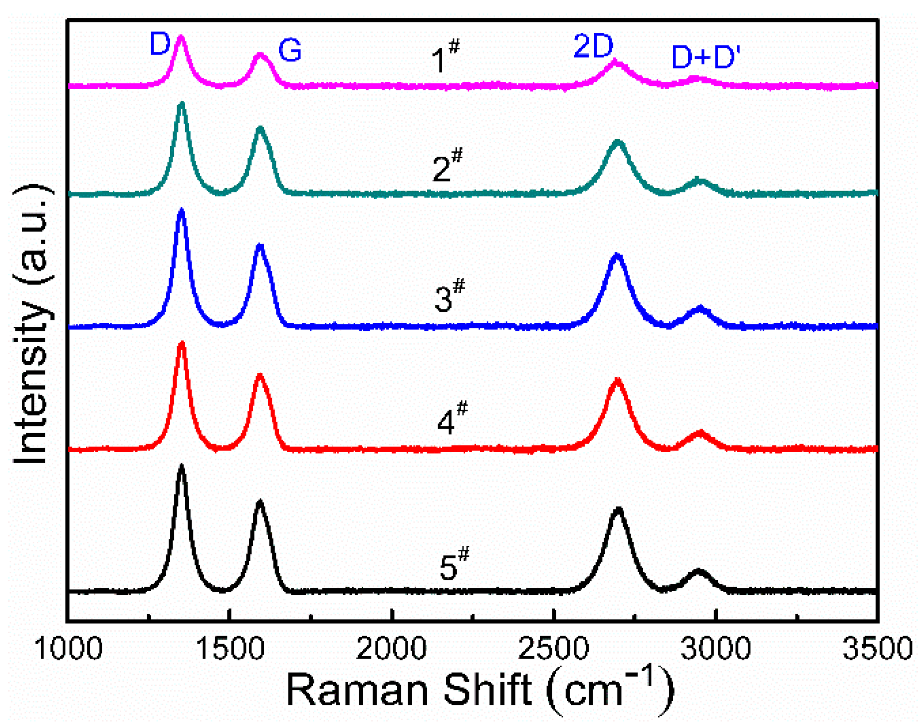
| Samples | D-Band Position | D-Band Intensity | G-Band Position | G-Band Intensity | 2D-Band Position | 2D-Band Intensity | ID/IG | I2D/IG |
|---|---|---|---|---|---|---|---|---|
| 1# | 1349 cm−1 | 3240 | 1598 cm−1 | 2103 | 2688 cm−1 | 1728 | 1.54 | 0.82 |
| 2# | 1354 cm−1 | 5922 | 1595 cm−1 | 4333 | 2690 cm−1 | 3426 | 1.37 | 0.79 |
| 3# | 1350 cm−1 | 7572 | 1592 cm−1 | 5262 | 2693 cm−1 | 4683 | 1.44 | 0.89 |
| 4# | 1354 cm−1 | 6913 | 1595 cm−1 | 4834 | 2693 cm−1 | 4528 | 1.43 | 0.94 |
| 5# | 1350 cm−1 | 8143 | 1595 cm−1 | 5849 | 2704 cm−1 | 5359 | 1.39 | 0.92 |
© 2018 by the authors. Licensee MDPI, Basel, Switzerland. This article is an open access article distributed under the terms and conditions of the Creative Commons Attribution (CC BY) license (http://creativecommons.org/licenses/by/4.0/).
Share and Cite
Wang, J.; Wang, X.; Yu, J.; Xiao, T.; Peng, L.; Fan, L.; Wang, C.; Shen, Q.; Wu, W. Tailoring the Grain Size of Bi-Layer Graphene by Pulsed Laser Deposition. Nanomaterials 2018, 8, 885. https://doi.org/10.3390/nano8110885
Wang J, Wang X, Yu J, Xiao T, Peng L, Fan L, Wang C, Shen Q, Wu W. Tailoring the Grain Size of Bi-Layer Graphene by Pulsed Laser Deposition. Nanomaterials. 2018; 8(11):885. https://doi.org/10.3390/nano8110885
Chicago/Turabian StyleWang, Jin, Xuemin Wang, Jian Yu, Tingting Xiao, Liping Peng, Long Fan, Chuanbin Wang, Qiang Shen, and Weidong Wu. 2018. "Tailoring the Grain Size of Bi-Layer Graphene by Pulsed Laser Deposition" Nanomaterials 8, no. 11: 885. https://doi.org/10.3390/nano8110885
APA StyleWang, J., Wang, X., Yu, J., Xiao, T., Peng, L., Fan, L., Wang, C., Shen, Q., & Wu, W. (2018). Tailoring the Grain Size of Bi-Layer Graphene by Pulsed Laser Deposition. Nanomaterials, 8(11), 885. https://doi.org/10.3390/nano8110885