Article

Physical Properties and Photovoltaic Application of Semiconducting Pd2Se3 Monolayer

1
Center for Applied Physics and Technology, HEDPS, Department of Materials Science and Engineering, College of Engineering, Peking University, Beijing 100871, China
2
Collaborative Innovation Center of IFSA (CICIFSA), Shanghai Jiao Tong University, Shanghai 200240, China
3
Institute for Advanced Study, Tsinghua University, Beijing 100084, China
*
Author to whom correspondence should be addressed.
Nanomaterials 2018, 8(10), 832; https://doi.org/10.3390/nano8100832
Submission received: 18 September 2018 / Revised: 4 October 2018 / Accepted: 13 October 2018 / Published: 14 October 2018

Abstract

:
Palladium selenides have attracted considerable attention because of their intriguing properties and wide applications. Motivated by the successful synthesis of Pd2Se3 monolayer (Lin et al., Phys. Rev. Lett., 2017, 119, 016101), here we systematically study its physical properties and device applications using state-of-the-art first principles calculations. We demonstrate that the Pd2Se3 monolayer has a desirable quasi-direct band gap (1.39 eV) for light absorption, a high electron mobility (140.4 cm2V−1s−1) and strong optical absorption (~105 cm−1) in the visible solar spectrum, showing a great potential for absorber material in ultrathin photovoltaic devices. Furthermore, its bandgap can be tuned by applying biaxial strain, changing from indirect to direct. Equally important, replacing Se with S results in a stable Pd2S3 monolayer that can form a type-II heterostructure with the Pd2Se3 monolayer by vertically stacking them together. The power conversion efficiency (PCE) of the heterostructure-based solar cell reaches 20%, higher than that of MoS2/MoSe2 solar cell. Our study would motivate experimental efforts in achieving Pd2Se3 monolayer-based heterostructures for new efficient photovoltaic devices.

Graphical Abstract

1. Introduction

Two-dimensional (2D) transition metal chalcogenides (TMCs), including semiconducting MoS2 [1], MoSe2 [2], WS2 [3], WSe2 [4], ReS2 [5], PtS2 [6], PdSe2 [7,8], and metallic VS2 [9] and NbS2 [10] are of current interest because of their extraordinary properties and practical applications in catalysis [11], electronics [12,13,14], optoelectronics [15,16] and valleytronics [17,18]. Among them, the layered PdSe2 has attracted special attention due to its unique atomic configuration and electronic properties [8,19,20]. Whereas previous studies mainly focused on the PdSe2 monolayer that has the same structural form as a single layer of the bulk PdSe2 [7,21,22]. Very recently, Lin et al. reported the successful exfoliation of a new monolayer phase with a stoichiometry of Pd2Se3 [23], and found that Se vacancies in the pristine PdSe2 reduce the distance between the layers, melding the two layers into one, thus, resulting in the formation of the Pd2Se3 monolayer. Due to its structural novelty, subsequent efforts have been made to further explore this new material, including its electronic and optical properties [24] and thermoelectric performance [25], as well as theoretical calculations and experimental synthesis of the lateral junctions between a PdSe2 bilayer and the Pd2Se3 monolayer [26].
We noticed that in Reference [24] the results were obtained from standard density functional theory (DFT) calculations (the Perdew-Burke-Ernzerhof (PBE) functional [27] for the generalized gradient approximation (GGA)), which is well-known to underestimate the electronic band gap of semiconductors. However, the accurate description of electronic structure is important for further investigation of electronic and optical properties. To overcome this limitation, various theoretical approaches have been developed. Among them, the hybrid functional that combines standard DFT with Hartree-Fock (HF) calculations has been widely used for calculating the band gaps, because it predicts more reliable physical properties and keeps a good compromise with computational efficiency. Therefore, we use the Heyd-Scuseria-Ernzerhof (HSE06) hybrid functional [28,29] to study the electronic, transport and optical properties of the newly synthesized Pd2Se3 monolayer. We show that this monolayer possesses a desirable bandgap for light harvesting, offering better opportunity for photovoltaic applications. Moreover, its electronic structure can be effectively tuned by applying biaxial strain, and indirect to direct bandgap transition occurs with a small critical strain of 2%. In addition, a stable Pd2S3 monolayer can be formed by substituting Se with S, which can be used to construct a type-II heterostructure with the Pd2Se3 monolayer. The heterostructure-based solar cell can reach a high power conversion efficiency (PCE) of 20%. These fascinating properties make the Pd2Se3 monolayer a promising candidate for future applications in nanoscale electronics and photonics.

2. Computational Methods

Within the framework of DFT, our first-principles calculations are performed using the projector augmented wave (PAW) method [30] as implemented in the Vienna Ab initio Simulation Package (VASP) [31]. The Perdew-Burke-Ernzerhof (PBE) functional [27] with the generalized gradient approximation (GGA) is used to treat the electron exchange-correlation interactions in crystal structure calculations, while the Heyd-Scuseria-Ernzerhof (HSE06) hybrid functional [28,29], which includes the Hartree-Fock exchange energy and the Coulomb screening effect, is used to calculate the electronic and optical properties. A kinetic energy cutoff of 350 eV is set for the plane wave basis. The convergence criteria are 10−5 eV and 10−3 eV/Å for total energy and atomic force components, respectively. The Brillouin zone is represented by k points with a grid density of 2π × 0.02 Å−1 in the reciprocal space using the Monkhorst-Pack scheme [32]. An adequate vacuum space (~20 Å) in the direction perpendicular to the sheet is used to minimize the interlayer interactions under the periodic boundary condition. Spin-orbit coupling (SOC) interactions are not included since our calculation shows that the SOC has negligible effect on electronic structure of the monolayer (see Figure S2). Phonon dispersion and density of states (DOS) are calculated using the finite displacement method [33] as implemented in the Phonopy code [34].
In the calculation of carrier mobility (µ), we consider the perfect crystal of the monolayer without defects and impurities. In addition, carrier mobility is a function of temperature. We set the temperature to be 300 K in our calculation, since most devices work at room temperature. In this situation, the dominant source of electron scattering is from acoustic phonons and the carrier mobility can be obtained using deformation potential theory proposed by Bardeen and Shockley [35], which has been successfully employed in many 2D materials [36,37,38,39]. Using effective mass approximation, the analytical expression of carrier mobility in 2D materials can be written as
μ = e 3 C k B T m * m d E 1 2  
C is the elastic modulus of the 2D sheet, T is the temperature, which is taken to be 300 K in our calculations, m* = ħ2[∂2E(k)/∂k2]−1 is the effective mass of the band edge carrier along the transport direction and md is the average effective mass determined by m d = m x * m y * . E1 is the DP constant defined as the energy shift of the band edge with respect to lattice dilation and compression, and kB and ħ are Boltzmann and reduced Planck constants, respectively.
The optical absorption coefficient (α) can be expressed as [40,41,42]
α ( ω ) = 2 ω [ ε 1 2 ( ω ) + ε 2 2 ( ω ) ε 1 ( ω ) ] 1 / 2  
where ε1(ω) and ε2(ω) are the real and imaginary parts of the frequency-dependent dielectric functions which are obtained using the time-dependent Hartree-Fock approach (TDHF) based on the HSE06 hybrid functional calculations [43]. The model, developed by Scharber et al. for organic solar cells [44] and exciton-based 2D solar cells [45,46,47,48,49], is used to calculate the maximum PCE in the limit of 100% external quantum efficiency (EQE), which can be written as
η = β F F V o c J s c P s o l a r = 0.65 ( E g d Δ E c 0.3 ) E g d P ( ϖ ) ϖ d ( ϖ ) 0 P ( ϖ ) d ( ϖ )  
Here, the fill factor β F F , which is the ratio of maximum power output to the product of the open-circuit voltage (Voc) and the short-circuit current (Jsc), is estimated to be 0.65 in this model. Voc (in eV) is estimated by the term ( E g d Δ E c 0.3 ), where E g d is the bandgap of the donor and Δ E c is the conduction band (CB) offset between donor and acceptor. Jsc is obtained by E g d P ( ϖ ) ϖ d ( ϖ ) , and the total incident solar power per unit area Psolar is equal to 0 P ( ϖ ) d ( ϖ ) . Here, ħ and ϖ are reduced Planck constants and photon frequency, and P(ϖ) is the air mass (AM) 1.5 solar energy flux (expressed in W m−2 eV−1) at the photon energy (ϖ).

3. Results and Discussion

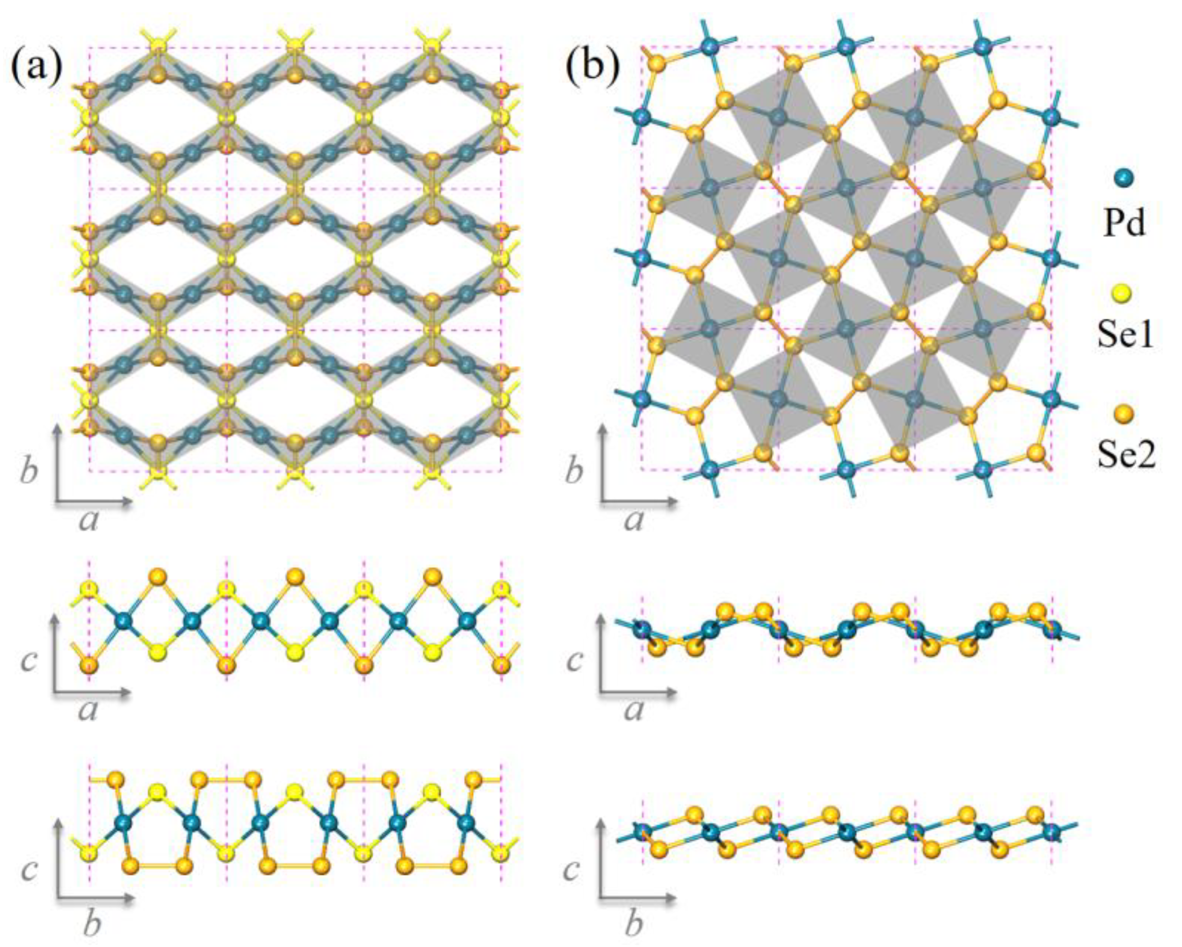
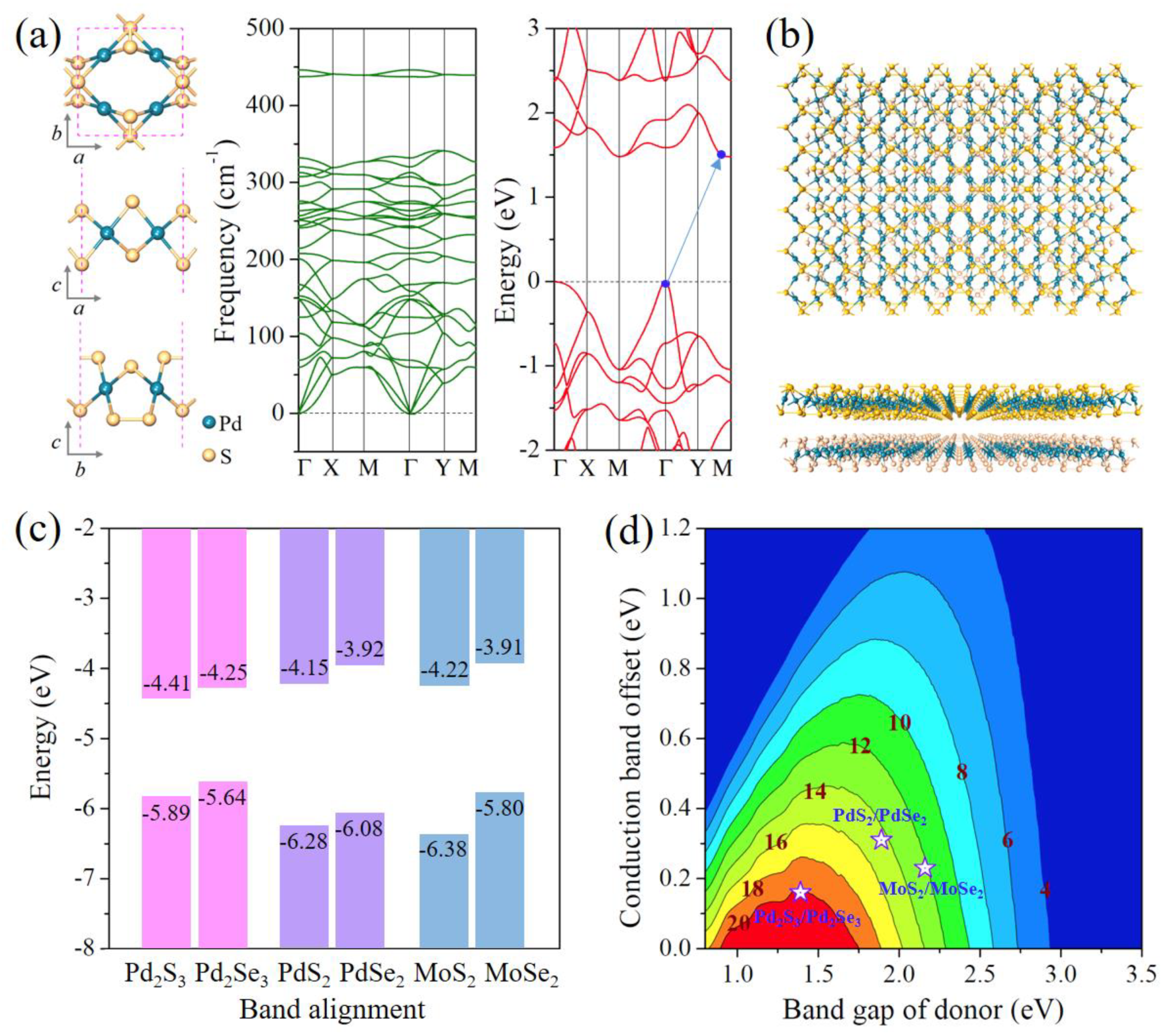
3.1. Geometric Structure of Pd2Se3

Figure 1a,b shows the optimized monolayer structures of Pd2Se3 and PdSe2 respectively (the structural details are listed in Table S1, Supplementary Materials). For simplicity, we refer these two monolayer structures as Pd2Se3 and PdSe2 in the following discussions unless stated otherwise. There are similarities as well as differences between the two structures. On one hand, they both consist of a layer of metal Pd atoms sandwiched between the two layers of chalcogen Se atoms, and each Pd atom binds to four Se atoms forming the square-planar (PdSe4) structural units. On the other hand, Pd2Se3 indeed distinguishes itself from PdSe2 in the following characteristics: (1) Pd2Se3 possesses Pmmn symmetry (point group D2h) with four Pd and six Se atoms in one unit cell. While the symmetry of PdSe2 is P21/c (point group C2h) and each unit cell contains two Pd and four Se atoms. The different crystal symmetries result in distinct resonance in the Raman spectroscopy, which can serve as an efficient and straightforward clue for experimentalists to confirm the formation of Pd2Se3. The details about the calculated Raman spectra of Pd2Se3 and PdSe2 are presented in the Supporting Information (Figure S1). (2) There are two chemically nonequivalent Se in Pd2Se3, marked in orange (Se2) and yellow (Se1) respectively. The two neighboring Se2 atoms form a covalent Se-Se bond while each Se1 atom is unpaired and binds to four neighboring Pd atoms. Whereas in PdSe2, all Se atoms are in dimers and form the Se-Se bonds. (3) In Pd2Se3, the Se-Se dumbbells are parallel to the Pd layer, while in PdSe2, they cross the Pd layer. (4) Pd2Se3 and PdSe2 have different charge-balanced formulas, written as (Pd2+)2(Se2−)(Se22−) and (Pd2+)(Se22−) respectively, due to the different chemical environments of Se atoms in the two structures. Since the properties of materials are essentially determined by their geometric structures, one can expect that Pd2Se3 would possess some new and different properties from those of PdSe2.

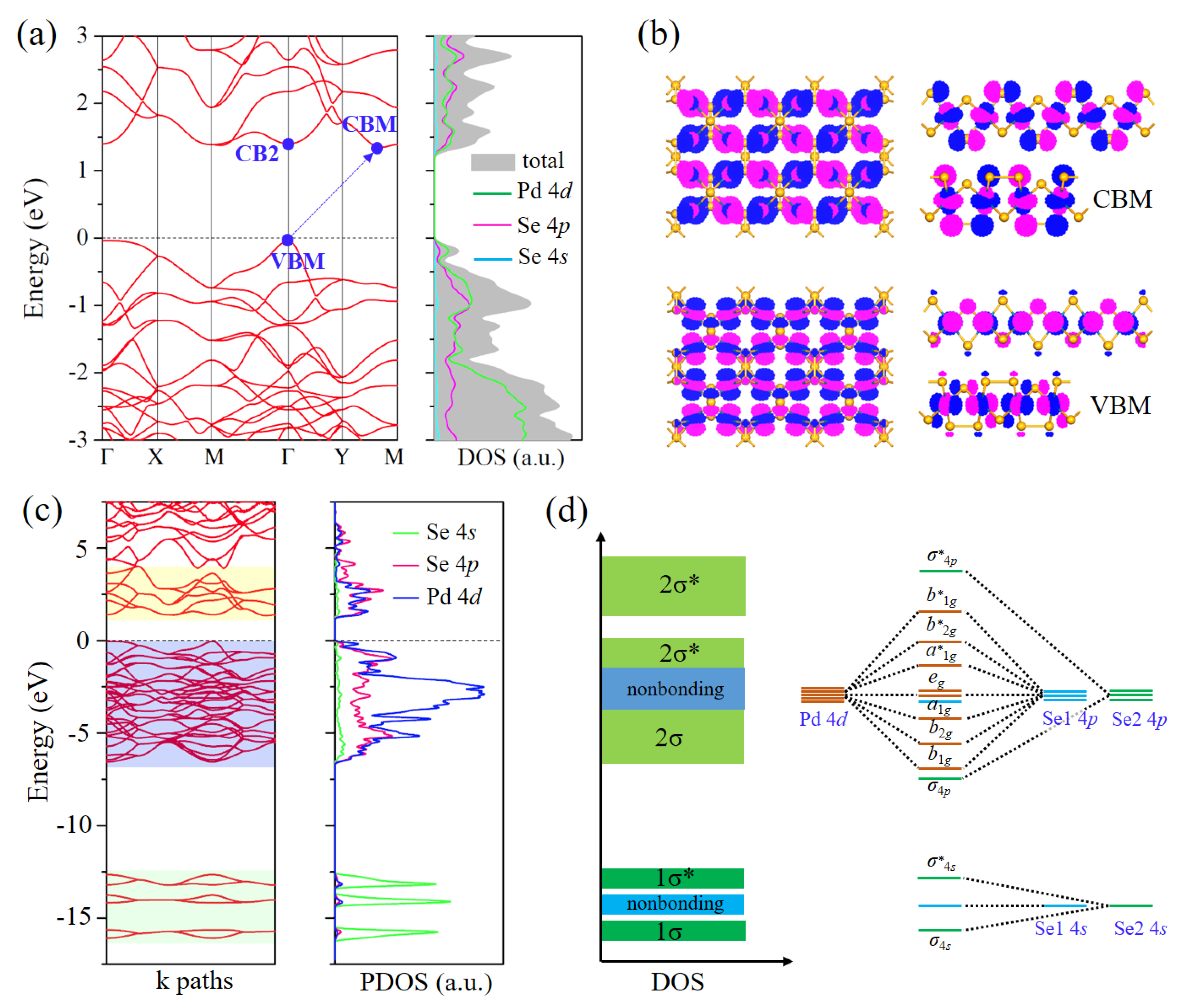
3.2. Electronic Properties of Pd2Se3

We then investigated the electronic properties of Pd2Se3 by calculating its electronic band structure and density of states (DOS) using the hybrid HSE06 functional. Figure 2a shows the calculated band structure around the Fermi level and corresponding total and partial DOS. The bandgap size of Pd2Se3 is 1.39 eV, close to the optimum value (~1.3 eV) for solar cell materials [50,51,52]. Although Pd2Se3 is an indirect bandgap semiconductor with the valence band maximum (VBM) located at the Γ point and the conduction band minimum (CBM) located on the Y-M path, Pd2Se3 can be considered as a quasi-direct bandgap semiconductor because of the existence of the sub-CBM at the Γ point (CB2) that is only marginally higher in energy than the true CBM (the energy difference is less than 50 meV). The weakly indirect bandgap is desirable for photovoltaic applications since it can simultaneously increase optical absorbance and photocarrier lifetimes [41,53,54]. To assess the effect of SOC interaction, we computed the band structure of Pd2Se3 at the level of HSE06+SOC. The results in Figure S2 reveal that the SOC in Pd2Se3 is weak and has negligible effect on the bandgap of this structure. Hereafter, we do not include the SOC interaction and just use the HSE06 scheme for calculations in this study.
An analysis of the partial DOS in Figure 2a indicates that the electronic states of valance and conduction bands mainly originate from Se 4p and Pd 4d orbitals. In addition, the overlap of the orbital-projected DOS implies strong hybridization, that is, the formation of covalent bonds between Se 4p and Pd 4d orbitals. By calculating wave functions for the VBM and CBM, we visualized their electronic states showing distinct antibonding features for both of them (see Figure 2b). However, to gain a better understanding for the covalent bonding in this 2D structure, the electronic bands not only limited to near the Fermi level but also in a large energy range should be taken into account.
Figure 2c displays the band structure and partial DOS including all occupied and sufficient unoccupied states of Pd2Se3. Combining crystal field theory and crystal structure chemistry analysis, we can clearly identify the electronic states in the energy range from −17 to 4 eV. From partial DOS, the bands in the energy range of −17 ~ −12.5 eV are primarily from Se 4s orbitals. According to the different bonding states, they can be classified into three groups. The bottom and upper subsets correspond to the bonding and antibonding states dominated by the formation of Se-Se bonds, and the middle part is the nonbonding state of the unpaired Se 4s orbitals. When the energy goes up, there occurs Pd 4d orbitals. In Pd2Se3, the Pd atom is coordinated in a nearly perfect square-planar geometry, and its 4d orbitals split into four energy levels, i.e., eg (dxz/dyz), a1g (dz2), b2g (dxy), and b1g (dx2-y2) from low to high energy. These d orbitals overlapping with Se 4p orbitals constitutes the bands in the energy range of −7.5 ~ 4 eV. In Figure 2d, we present the schematic drawing of DOS and energy level diagram of Pd2Se3 to explain details about how Pd 4d orbitals interact with Se 4p orbitals. It shows that a1g, b2g, and b1g orbitals hybridize with Se 4p orbitals leading to lower energy bonding states and higher energy antibonding states, whereas the nonbonding states in the energy range from −4 to −1.7 eV stemming mainly from eg orbitals. More importantly, the bandgap that separates occupied and unoccupied states lies in the antibonding region and amounts to the splitting energy between and states, consistent with the results of wave functions for the VBM and CBM in Figure 2b. The systematic and deep exploration of electronic structure of Pd2Se­3 is crucial for understanding its properties and origins of intriguing physical phenomena.

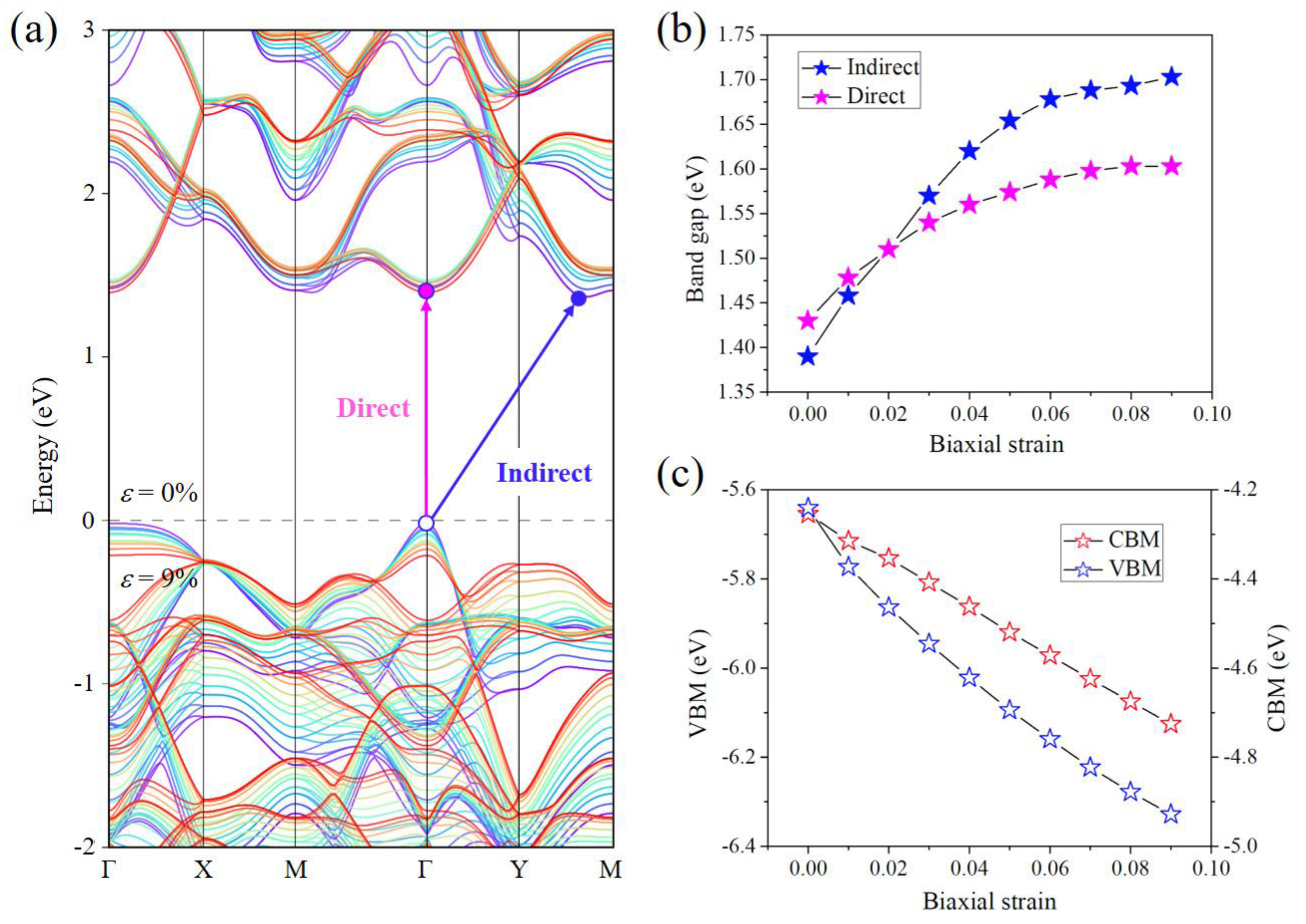
3.3. Strain Engineering of Electronic Band Structure of Pd2Se3

From above electronic structure analysis, it is clear that Pd2Se3 is a covalent semiconductor, and a connection between elastic strain and its electronic structure is expected. This is because elastic strain generally weakens the covalent interaction as the bonds lengthen, exerting efficient modulation on the band energies and bandgap. For this reason, we applied a biaxial tensile strain to Pd2Se3 and study its effect on the electronic bands of Pd2Se3.
Figure 3a shows the evolution of band structure with biaxial strain varying from 0% to 9%. It indicates that both direct and indirect bandgaps increase, and a transition from indirect bandgap to direct bandgap occurs when the biaxial strain is applied. To acquire a more accurate energy profile, we present the strain-dependent bandgaps in Figure 3b, which clearly shows the increasing trend of bandgaps and the bandgap transition from indirect to direct at the critical strain of 2%.
The strain-dependent bandgap of Pd2Se3 can be understood by analyzing its electronic structure in Figure 2, which shows that the valence and conduction bands both originate from antibonding states. Application of a tensile strain increases the Pd–Se bond length thus decreases the amount of orbital overlap, leading to the stabilization of valence and conduction bands and reducing them in energy. This is consistent with our results, as shown in Figure 3c, which displays the strain-dependent energy levels for the VBM and CBM. However, since the biaxial tensile strain not only enlarges the bond length but also distorts the square-planar ligand field (see Figure S3 for details), the valence band responds more strongly to strains than the conduction band, resulting in the increase of bandgap in the imposed strain filed.
Additionally, we also examined the structural stability under biaxial strains. The phonon dispersion in Figure S4 demonstrates that the structure remains stable under the strain of 9%. The large strain tolerance and an electronic structure that has a continuous response in the imposed strain field indicate the great potential of Pd2Se3 in future flexible electronics.

3.4. Transport Properties of Pd2Se3

We also investigated the transport properties of Pd2Se3 by calculating its room-temperature carrier mobilities as summarized in Table 1. One can see that the mobilities for both electrons and holes are slightly anisotropic along the x and y directions, due to the structural anisotropy of Pd2Se3. Meanwhile, the electron mobility along the y direction is estimated to be 140.4 cm2V−1s−1, significantly higher than that of hole. When compared with PdSe2, whose carrier mobilities are calculated at the same theoretical level and listed in Table 1, Pd2Se3 possesses higher electron mobility and lower hole mobility, showing strong asymmetry in electron and hole transport. Although the carrier mobilities of Pd2Se3 is lower than the theoretical predicted carrier mobilities of some other 2D materials [36,38,55], it is still commendable if realized in practice [20].

3.5. Optical Properties of Pd2Se3

Attracted by the suitable bandgap and intriguing electronic properties of Pd2Se3, we further explored its light-harvesting performance by calculating the dielectric functions based on the hybrid HSE06 functional. Figure 4a shows the real (ε1) and imaginary (ε2) parts of the frequency-dependent complex dielectric functions of Pd2Se3. With the dielectric functions, we derive its optical absorption coefficient (α), as shown in Figure 4b. For comparison, the absorption spectra of PdSe2 was also calculated. We notice that, for both Pd2Se3 and PdSe2, the overall absorption coefficients are close to the order of 105 cm−1 and only show little difference along the x and y directions, which are considerably desirable for optical absorption. Moreover, as shown in Figure 4b, the absorption coefficient of Pd2Se3 is slightly larger than that of PdSe2 in nearly the entire of the energy range, indicating the improved light-harvesting performance of Pd2Se3 as compared with PdSe2. Furthermore, we also investigated the biaxial strain influence on the optical performance of Pd2Se3. The calculated strain-dependent optical absorption spectra are presented in Figure 4c. It shows that the strain slightly affects the optical absorption of Pd2Se3, which is favorable for applications in flexible systems since it guarantees steady performance of devices under stretching.

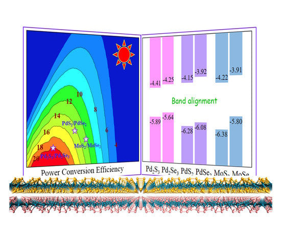
3.6. Extension and Photovoltaic Application of Pd2Se3

Moreover, we further explored the feasibility of other Pd2X3 monolayer phases, with X to be S and Te, respectively. Bulk PdS2 has the same geometrical structure as that of bulk PdSe2, thus the Pd2S3 monolayer might be experimentally synthesized following the same synthetic method as that of the Pd2Se3 monolayer. However, bulk PdTe2 prefers a 1T configuration, indicating that the Pd2Te3 monolayer might be inaccessible. To confirm our assumption, we calculated the phonon dispersions of the two structures. No imaginary mode exists in the phonon spectra of Pd2S3 (see Figure 5a), indicating its dynamical stability of the monolayer. Whereas the phonon spectra of the Pd2Te3 monolayer shows imaginary frequency near the Γ point (see Figure S5), demonstrating its structural instability. We then calculated the electronic band structure of the stable Pd2S3 monolayer (Figure 5a), verifying the feature of a semiconductor with an indirect bandgap of 1.48 eV.
Since 2D TMCs can be vertically stacked layer-by-layer forming the van der Waals heterostructures which can efficiently modulate properties of materials for applications in nanoscale electronic and photovoltaic devices, here we propose a van der Waals heterostructure composed of the Pd2Se3 and Pd2S3 monolayers (see Figure 5b) and study its interesting properties. A key indicator for heterostructures is the band alignment that defines the type of heterostructures. Thus, we calculated the band alignment of the Pd2Se3 and Pd2S3 monolayers, as shown in Figure 5c. One can see that the Pd2S3/Pd2Se3 heterostructure has a type-II (ladder) band alignment, which allows more efficient electron-hole separation for lighting harvesting. Such type-II heterostructure can be used as active materials in excitonic solar cells (XSCs) [46,47,48,49]. For the Pd2S3/Pd2Se3 heterostructure, the Pd2Se3 monolayer is the donor and the Pd­2S3 monolayer serves as the acceptor. With the approximation that the HSE06 bandgap equals optical bandgap and using the model developed by Scharber et al. [44], we obtained the upper limit of the PCE, reaching as high as 20% (Figure 5d). For comparison, we also calculated the band alignments for the PdS2/PdSe2 and MoS2/MoSe2 heterostructures, and find that they both are type-II heterostructures with predicted PCEs to be 14% and 12% respectively. The high PCE of the Pd2S3/Pd2Se3 heterostructure renders it a promising candidate in flexible optoelectronic and photovoltaic devices.

4. Conclusions

In summary, on the basis of DFT calculations, we systematically studied the properties and potential applications of the recently synthesized Pd2Se3 monolayer by focusing on its geometric structure, electronic band structure, and optical adsorption. Comparing with the previously reported PdSe2 monolayer, we found that the Pd2Se3 monolayer has the following merits: (1) A suitable quasi-direct bandgap (1.39 eV) for light absorption, (2) a higher electron mobility (140.4 cm2V−1s−1) and (3) a stronger optical absorption (~ 105 cm−1) in the visible solar spectrum, showing promise of Pd2Se3 as an absorber material for future ultrathin photovoltaic devices. In addition, the Pd2Se3 monolayer combining with the stable Pd2S3 monolayer can form a type-II heterostructure, and the heterostructure solar cell system can achieve a 20% PCE. These findings would encourage experimentalists to devote more effort in developing Pd2Se3-based devices with high performance.

Supplementary Materials

The following are available online at https://www.mdpi.com/2079-4991/8/10/832/s1, Table S1: Structural parameters of the Pd2Se3, Pd2S3, Pd2Te3, PdS2, PdSe2, MoS2, and MoSe2 monolayers; Figure S1: (a) Raman spectra of PdSe2 and Pd2Se3 monolayers. (b) and (c) are the corresponding Raman-active vibrational modes of the two structures; Figure S2: Electronic band structure of the Pd2Se3 monolayer calculated at the HSE06 level with and without considering the SOC interaction; Figure S3: Geometric structure of the Pd2Se3 monolayer under 0% and 9% biaxial tensile strain; Figure S4: Phonon dispersion of the Pd2Se3 monolayer under 9% biaxial tensile strain; Figure S5: Phonon dispersion of the Pd2Te3 monolayer.

Author Contributions

Investigation, X.L.; Methodology, X.L., S.Z. and Y.G.; Supervision, Q.W.; Writing—original draft, X.L.; Writing—review & editing, X.L., S.Z., Y.G., F.Q.W. and Q.W.

Funding

This work is partially supported by grants from the National Key Research and Development Program of China (2016YFE0127300, and 2017YFA0205003), the National Natural Science Foundation of China (NSFC-51471004, and NSFC-21773004). S. Z. is supported by the National Postdoctoral Program for Innovative Talents of China (BX201600091) and the Funding from China Postdoctoral Science Foundation (2017M610858).

Acknowledgments

This work is also supported by the High Performance Computing Platform of Peking University, China.

Conflicts of Interest

The authors declare no conflict of interest.

References

  1. Lee, Y.H.; Zhang, X.Q.; Zhang, W.; Chang, M.T.; Lin, C.T.; Chang, K.D.; Yu, Y.C.; Wang Jacob, T.W.; Chang, C.S.; Li, L.J.; et al. Synthesis of Large-Area MoS2 Atomic Layers with Chemical Vapor Deposition. Adv. Mater. 2012, 24, 2320–2325. [Google Scholar] [CrossRef] [PubMed]
  2. Lu, X.; Utama, M.I.B.; Lin, J.; Gong, X.; Zhang, J.; Zhao, Y.; Pantelides, S.T.; Wang, J.; Dong, Z.; Liu, Z.; et al. Large-Area Synthesis of Monolayer and Few-Layer MoSe2 Films on SiO2 Substrates. Nano Lett. 2014, 14, 2419–2425. [Google Scholar] [CrossRef] [PubMed]
  3. Xu, Z.-Q.; Zhang, Y.; Lin, S.; Zheng, C.; Zhong, Y.L.; Xia, X.; Li, Z.; Sophia, P.J.; Fuhrer, M.S.; Cheng, Y.-B.; et al. Synthesis and Transfer of Large-Area Monolayer WS2 Crystals: Moving toward the Recyclable Use of Sapphire Substrates. ACS Nano 2015, 9, 6178–6187. [Google Scholar] [CrossRef] [PubMed]
  4. Huang, J.-K.; Pu, J.; Hsu, C.-L.; Chiu, M.-H.; Juang, Z.-Y.; Chang, Y.-H.; Chang, W.-H.; Iwasa, Y.; Takenobu, T.; Li, L.-J. Large-Area Synthesis of Highly Crystalline WSe2 Monolayers and Device Applications. ACS Nano 2014, 8, 923–930. [Google Scholar] [CrossRef] [PubMed]
  5. Lin, Y.-C.; Komsa, H.-P.; Yeh, C.-H.; Björkman, T.; Liang, Z.-Y.; Ho, C.-H.; Huang, Y.-S.; Chiu, P.-W.; Krasheninnikov, A.V.; Suenaga, K. Single-Layer ReS2: Two-Dimensional Semiconductor with Tunable in-Plane Anisotropy. ACS Nano 2015, 9, 11249–11257. [Google Scholar] [CrossRef] [PubMed]
  6. Zhao, Y.; Qiao, J.; Yu, P.; Hu, Z.; Lin, Z.; Lau, S.P.; Liu, Z.; Ji, W.; Chai, Y. Extraordinarily Strong Interlayer Interaction in 2D Layered PtS2. Adv. Mater. 2016, 28, 2399–2407. [Google Scholar] [CrossRef] [PubMed]
  7. Sun, J.; Shi, H.; Siegrist, T.; Singh, D.J. Electronic, Transport, and Optical Properties of Bulk and Mono-Layer PdSe2. Appl. Phys. Lett. 2015, 107, 153902. [Google Scholar] [CrossRef]
  8. Oyedele, A.D.; Yang, S.; Liang, L.; Puretzky, A.A.; Wang, K.; Zhang, J.; Yu, P.; Pudasaini, P.R.; Ghosh, A.W.; Liu, Z.; et al. PdSe2: Pentagonal Two-Dimensional Layers with High Air Stability for Electronics. J. Am. Chem. Soc. 2017, 139, 14090–14097. [Google Scholar] [CrossRef] [PubMed]
  9. Feng, J.; Sun, X.; Wu, C.; Peng, L.; Lin, C.; Hu, S.; Yang, J.; Xie, Y. Metallic Few-Layered VS2 Ultrathin Nanosheets: High Two-Dimensional Conductivity for in-Plane Supercapacitors. J. Am. Chem. Soc. 2011, 133, 17832–17838. [Google Scholar] [CrossRef] [PubMed]
  10. Zhao, S.; Hotta, T.; Koretsune, T.; Watanabe, K.; Taniguchi, T.; Sugawara, K.; Takahashi, T.; Shinohara, H.; Kitaura, R. Two-Dimensional Metallic NbS2: Growth, Optical Identification and Transport Properties. 2D Mater. 2016, 3, 025027. [Google Scholar] [CrossRef]
  11. Voiry, D.; Yang, J.; Chhowalla, M. Recent Strategies for Improving the Catalytic Activity of 2D TMD Nanosheets toward the Hydrogen Evolution Reaction. Adv. Mater. 2016, 28, 6197–6206. [Google Scholar] [CrossRef] [PubMed]
  12. Radisavljevic, B.; Radenovic, A.; Brivio, J.; Giacometti, V.; Kis, A. Single-Layer MoS2 Transistors. Nat. Nanotechnol. 2011, 6, 147. [Google Scholar] [CrossRef] [PubMed]
  13. Akinwande, D.; Petrone, N.; Hone, J. Two-Dimensional Flexible Nanoelectronics. Nat. Commun. 2014, 5, 5678. [Google Scholar] [CrossRef] [PubMed]
  14. Wang, H.; Yu, L.; Lee, Y.-H.; Shi, Y.; Hsu, A.; Chin, M.L.; Li, L.-J.; Dubey, M.; Kong, J.; Palacios, T. Integrated Circuits Based on Bilayer MoS2 Transistors. Nano Lett. 2012, 12, 4674–4680. [Google Scholar] [CrossRef] [PubMed]
  15. Yin, Z.; Li, H.; Li, H.; Jiang, L.; Shi, Y.; Sun, Y.; Lu, G.; Zhang, Q.; Chen, X.; Zhang, H. Single-Layer MoS2 Phototransistors. ACS Nano 2012, 6, 74–80. [Google Scholar] [CrossRef] [PubMed]
  16. Lopez-Sanchez, O.; Lembke, D.; Kayci, M.; Radenovic, A.; Kis, A. Ultrasensitive Photodetectors Based on Monolayer MoS2. Nat. Nanotechnol. 2013, 8, 497. [Google Scholar] [CrossRef] [PubMed]
  17. Mak, K.F.; He, K.; Shan, J.; Heinz, T.F. Control of Valley Polarization in Monolayer MoS2 by Optical Helicity. Nat. Nanotechnol. 2012, 7, 494. [Google Scholar] [CrossRef] [PubMed]
  18. Cao, T.; Wang, G.; Han, W.; Ye, H.; Zhu, C.; Shi, J.; Niu, Q.; Tan, P.; Wang, E.; Liu, B.; et al. Valley-Selective Circular Dichroism of Monolayer Molybdenum Disulphide. Nat. Commun. 2012, 3, 887. [Google Scholar] [CrossRef] [PubMed]
  19. Soulard, C.; Rocquefelte, X.; Petit, P.E.; Evain, M.; Jobic, S.; Itié, J.P.; Munsch, P.; Koo, H.J.; Whangbo, M.H. Experimental and Theoretical Investigation on the Relative Stability of the PdS2- and Pyrite-Type Structures of PdSe2. Inorg. Chem. 2004, 43, 1943–1949. [Google Scholar] [CrossRef] [PubMed]
  20. Chow, W.L.; Yu, P.; Liu, F.; Hong, J.; Wang, X.; Zeng, Q.; Hsu, C.H.; Zhu, C.; Zhou, J.; Wang, X.; et al. High Mobility 2D Palladium Diselenide Field-Effect Transistors with Tunable Ambipolar Characteristics. Adv. Mater. 2017, 29, 1602969. [Google Scholar] [CrossRef] [PubMed]
  21. Lebègue, S.; Björkman, T.; Klintenberg, M.; Nieminen, R.M.; Eriksson, O. Two-Dimensional Materials from Data Filtering and Ab Initio Calculations. Phys. Rev. X 2013, 3, 031002. [Google Scholar]
  22. Wang, Y.; Li, Y.; Chen, Z. Not Your Familiar Two Dimensional Transition Metal Disulfide: Structural and Electronic Properties of the PdS2 Monolayer. J. Mater. Chem. C 2015, 3, 9603–9608. [Google Scholar] [CrossRef]
  23. Lin, J.; Zuluaga, S.; Yu, P.; Liu, Z.; Pantelides, S.T.; Suenaga, K. Novel Pd2Se3 Two-Dimensional Phase Driven by Interlayer Fusion in Layered PdSe2. Phys. Rev. Lett. 2017, 119, 016101. [Google Scholar] [CrossRef] [PubMed]
  24. Zhu, X.; Li, F.; Wang, Y.; Qiao, M.; Li, Y. Pd2Se3 Monolayer: A Novel Two-Dimensional Material with Excellent Electronic, Transport, and Optical Properties. J. Mater. Chem. C 2018, 6, 4494–4500. [Google Scholar] [CrossRef]
  25. Naghavi, S.S.; He, J.; Xia, Y.; Wolverton, C. Pd2Se3 Monolayer: A Promising Two-Dimensional Thermoelectric Material with Ultralow Lattice Thermal Conductivity and High Power Factor. Chem. Mater. 2018, 30, 5639–5647. [Google Scholar] [CrossRef]
  26. Sebastian, Z.; Junhao, L.; Kazu, S.; Sokrates, T.P. Two-Dimensional PdSe2-Pd2Se3 Junctions Can Serve as Nanowires. 2D Mater. 2018, 5, 035025. [Google Scholar]
  27. Perdew, J.P.; Burke, K.; Ernzerhof, M. Generalized Gradient Approximation Made Simple. Phys. Rev. Lett. 1996, 77, 3865–3868. [Google Scholar] [CrossRef] [PubMed]
  28. Heyd, J.; Scuseria, G.E.; Ernzerhof, M. Hybrid Functionals Based on a Screened Coulomb Potential. J. Chem. Phys. 2003, 118, 8207–8215. [Google Scholar] [CrossRef]
  29. Heyd, J.; Scuseria, G.E.; Ernzerhof, M. Erratum: “Hybrid Functionals Based on a Screened Coulomb Potential” [J. Chem. Phys. 118, 8207 (2003)]. J. Chem. Phys. 2006, 124, 219906. [Google Scholar] [CrossRef]
  30. Blöchl, P.E. Projector Augmented-Wave Method. Phys. Rev. B 1994, 50, 17953–17979. [Google Scholar] [CrossRef]
  31. Kresse, G.; Furthmüller, J. Efficient Iterative Schemes for Ab Initio Total-Energy Calculations Using a Plane-Wave Basis Set. Phys. Rev. B 1996, 54, 11169–11186. [Google Scholar] [CrossRef]
  32. Monkhorst, H.J.; Pack, J.D. Special Points for Brillouin-Zone Integrations. Phys. Rev. B 1976, 13, 5188–5192. [Google Scholar] [CrossRef]
  33. Parlinski, K.; Li, Z.Q.; Kawazoe, Y. First-Principles Determination of the Soft Mode in Cubic ZrO2. Phys. Rev. Lett. 1997, 78, 4063–4066. [Google Scholar] [CrossRef]
  34. Togo, A.; Tanaka, I. First Principles Phonon Calculations in Materials Science. Scripta Mater. 2015, 108, 1–5. [Google Scholar] [CrossRef] [Green Version]
  35. Bardeen, J.; Shockley, W. Deformation Potentials and Mobilities in Non-Polar Crystals. Phys. Rev. 1950, 80, 72–80. [Google Scholar] [CrossRef]
  36. Qiao, J.; Kong, X.; Hu, Z.-X.; Yang, F.; Ji, W. High-Mobility Transport Anisotropy and Linear Dichroism in Few-Layer Black Phosphorus. Nat. Commun. 2014, 5, 4475. [Google Scholar] [CrossRef] [PubMed]
  37. Cai, Y.; Zhang, G.; Zhang, Y.-W. Polarity-Reversed Robust Carrier Mobility in Monolayer MoS2 Nanoribbons. J. Am. Chem. Soc. 2014, 136, 6269–6275. [Google Scholar] [CrossRef] [PubMed]
  38. Dai, J.; Zeng, X.C. Titanium Trisulfide Monolayer: Theoretical Prediction of a New Direct-Gap Semiconductor with High and Anisotropic Carrier Mobility. Angew. Chem. Int. Ed. 2015, 54, 7572–7576. [Google Scholar] [CrossRef] [PubMed] [Green Version]
  39. Jing, Y.; Ma, Y.; Li, Y.; Heine, T. GeP3: A Small Indirect Band Gap 2d Crystal with High Carrier Mobility and Strong Interlayer Quantum Confinement. Nano Lett. 2017, 17, 1833–1838. [Google Scholar] [CrossRef] [PubMed]
  40. Saha, S.; Sinha, T.P.; Mookerjee, A. Electronic Structure, Chemical Bonding, and Optical Properties of Paraelectric BaTiO3. Phys. Rev. B 2000, 62, 8828–8834. [Google Scholar] [CrossRef]
  41. Miao, N.; Xu, B.; Bristowe, N.C.; Zhou, J.; Sun, Z. Tunable Magnetism and Extraordinary Sunlight Absorbance in Indium Triphosphide Monolayer. J. Am. Chem. Soc. 2017, 139, 11125–11131. [Google Scholar] [CrossRef] [PubMed]
  42. Wang, B.; Niu, X.; Ouyang, Y.; Zhou, Q.; Wang, J. Ultrathin Semiconducting Bi2Te2S and Bi2Te2Se with High Electron Mobilities. J. Phys. Chem. Lett. 2018, 9, 487–490. [Google Scholar] [CrossRef] [PubMed]
  43. Paier, J.; Marsman, M.; Kresse, G. Dielectric Properties and Excitons for Extended Systems from Hybrid Functionals. Phys. Rev. B 2008, 78, 121201. [Google Scholar] [CrossRef]
  44. Scharber, M.C.; Mühlbacher, D.; Koppe, M.; Denk, P.; Waldauf, C.; Heeger, A.J.; Brabec, C.J. Design Rules for Donors in Bulk-Heterojunction Solar Cells-Towards 10 % Energy-Conversion Efficiency. Adv. Mater. 2006, 18, 789–794. [Google Scholar] [CrossRef]
  45. Bernardi, M.; Palummo, M.; Grossman, J.C. Semiconducting Monolayer Materials as a Tunable Platform for Excitonic Solar Cells. ACS Nano 2012, 6, 10082–10089. [Google Scholar] [CrossRef] [PubMed] [Green Version]
  46. Dai, J.; Zeng, X.C. Bilayer Phosphorene: Effect of Stacking Order on Bandgap and Its Potential Applications in Thin-Film Solar Cells. J. Phys. Chem. Lett. 2014, 5, 1289–1293. [Google Scholar] [CrossRef] [PubMed] [Green Version]
  47. Ganesan, V.D.S.O.; Linghu, J.; Zhang, C.; Feng, Y.P.; Shen, L. Heterostructures of Phosphorene and Transition Metal Dichalcogenides for Excitonic Solar Cells: A First-Principles Study. Appl. Phys. Lett. 2016, 108, 122105. [Google Scholar] [CrossRef]
  48. Xie, M.; Zhang, S.; Cai, B.; Huang, Y.; Zou, Y.; Guo, B.; Gu, Y.; Zeng, H. A Promising Two-Dimensional Solar Cell Donor: Black Arsenic–Phosphorus Monolayer with 1.54 eV Direct Bandgap and Mobility Exceeding 14,000 cm2v−1s−1. Nano Energy 2016, 28, 433–439. [Google Scholar] [CrossRef]
  49. Lee, J.; Huang, J.; Sumpter, B.G.; Yoon, M. Strain-Engineered Optoelectronic Properties of 2D Transition Metal Dichalcogenide Lateral Heterostructures. 2D Mater. 2017, 4, 021016. [Google Scholar] [CrossRef]
  50. Shockley, W.; Queisser, H.J. Detailed Balance Limit of Efficiency of P-N Junction Solar Cells. J. Appl. Phys. 1961, 32, 510–519. [Google Scholar] [CrossRef]
  51. Hanna, M.C.; Nozik, A.J. Solar Conversion Efficiency of Photovoltaic and Photoelectrolysis Cells with Carrier Multiplication Absorbers. J. Appl. Phys. 2006, 100, 074510. [Google Scholar] [CrossRef]
  52. Wadia, C.; Alivisatos, A.P.; Kammen, D.M. Materials Availability Expands the Opportunity for Large-Scale Photovoltaics Deployment. Environ. Sci. Technol. 2009, 43, 2072–2077. [Google Scholar] [CrossRef] [PubMed]
  53. Motta, C.; El-Mellouhi, F.; Kais, S.; Tabet, N.; Alharbi, F.; Sanvito, S. Revealing the Role of Organic Cations in Hybrid Halide Perovskite CH3NH3PbI3. Nat. Commun. 2015, 6, 7026. [Google Scholar] [CrossRef] [PubMed]
  54. Zheng, F.; Tan, L.Z.; Liu, S.; Rappe, A.M. Rashba Spin–Orbit Coupling Enhanced Carrier Lifetime in CH3NH3PbI3. Nano Lett. 2015, 15, 7794–7800. [Google Scholar] [CrossRef] [PubMed]
  55. Zhang, C.; Sun, Q. A Honeycomb BeN2 Sheet with a Desirable Direct Bandgap and High Carrier Mobility. J. Phys. Chem. Lett. 2016, 7, 2664–2670. [Google Scholar] [CrossRef] [PubMed]
Figure 1. Optimized atomic structure of (a) Pd2Se3, and (b) PdSe2 monolayers. The gray tetragons and purple dashed rectangles correspond to the planar (PdSe4) units and the primitive cells of the two structures, respectively.
Nanomaterials 08 00832 g001
Figure 2. (a) Band structure and DOS around the Fermi level. The VBM and CB(M) are marked by blue dots; (b) Spatial visualization of wave functions for the VBM and CBM, using an isosurface of 0.04 eÅ−3; (c) Band structure and partial DOS with all valence states included. (d) Schematics of DOS and energy level diagram.
Nanomaterials 08 00832 g002
Figure 3. (a) Electronic band structure of the Pd2Se3 monolayer under biaxial strains varying from 0% (violet line) to 9% (red line); (b) Direct and indirect bandgaps under different biaxial strains; (c) Biaxial strain-dependent energies of the VBM and CBM with respect to the vacuum level. All calculations are based on the HSE06 functional.
Nanomaterials 08 00832 g003
Figure 4. (a) Real part (ε1) and imaginary part (ε2) of the complex dielectric function, and (b) optical absorption spectra of Pd2Se3, as compared to those of PdSe2 along the x and y directions respectively; (c) Optical absorption spectra of Pd2Se3 under different biaxial strains from 0% (violet line) to 9% (red line).
Nanomaterials 08 00832 g004
Figure 5. (a) Optimized atomic structure, phonon spectra and electronic band structure (at the HSE06 level) of the Pd2S3 monolayer; (b) Top and side views of the heterostructure composed of the Pd2S3 and Pd2Se3 monolayers; (c) Band alignments of the Pd2S3, Pd2Se3, PdS2, PdSe2, MoS2, and MoSe2 monolayers calculated using the HSE06 functional. The numbers are the CBM and VBM energies with respect to the vacuum level, which is set to zero when calculating the band alignment diagrams; (d) Computed PCE contour as a function of the donor bandgap and conduction band offset. Violet open stars mark the PCEs of Pd2S3/Pd2Se3, PdS2/PdSe2, and MoS2/MoSe2 heterostructure solar cells.
Nanomaterials 08 00832 g005
Table 1. Calculated deformation potential constant (E1), elastic modulus (C), effective mass (m*), and mobility (μ) for electron and hole in the x and y directions for Pd2Se3 and PdSe2 monolayers at 300 K.
Carrier TypeE1 (eV)C (N/m)m* (me) μ (cm2V−1s−1)
Pd2Se3electron (x)3.75633.020.762101.9
electron (y)3.78532.930.543140.4
hole (x)2.87033.029.0297.3
hole (y)12.08232.930.18719.9
PdSe2electron (x)9.54232.450.42943.36
electron (y)9.98255.050.39073.99
hole (x)3.35232.450.65697.94
hole (y)3.07455.051.40192.54

