Overview of Phase-Change Electrical Probe Memory

Abstract
:1. Introduction
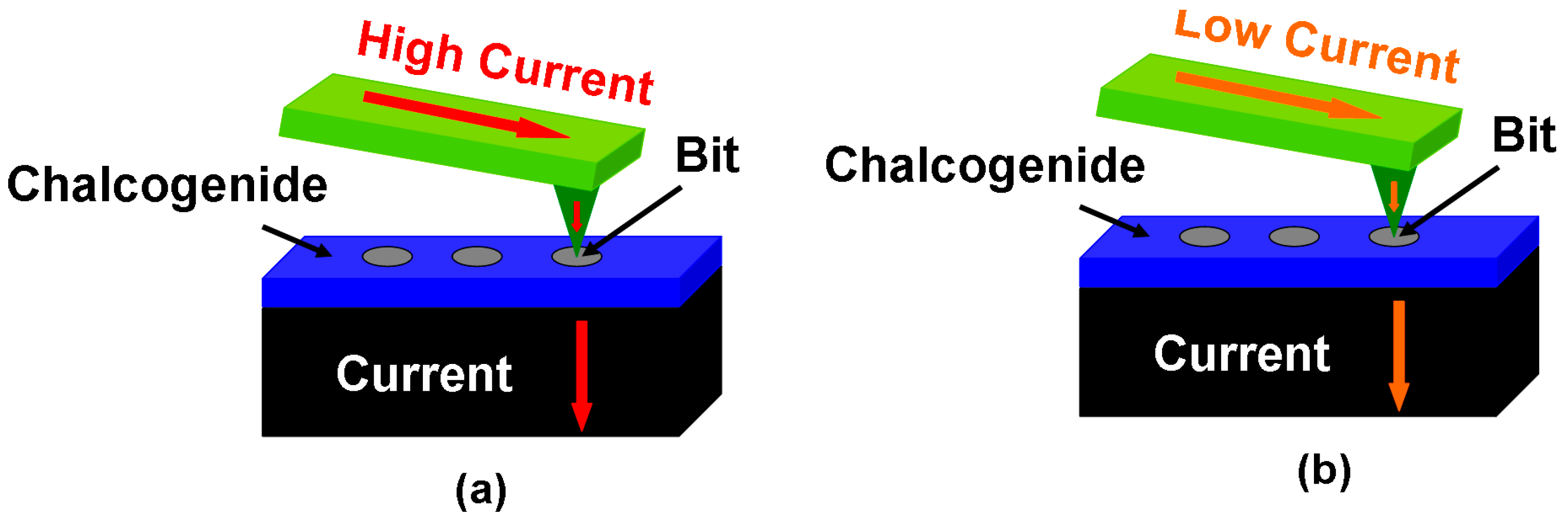
2. Storage Mechanisms Review of Phase-Change Electrical Probe Memory
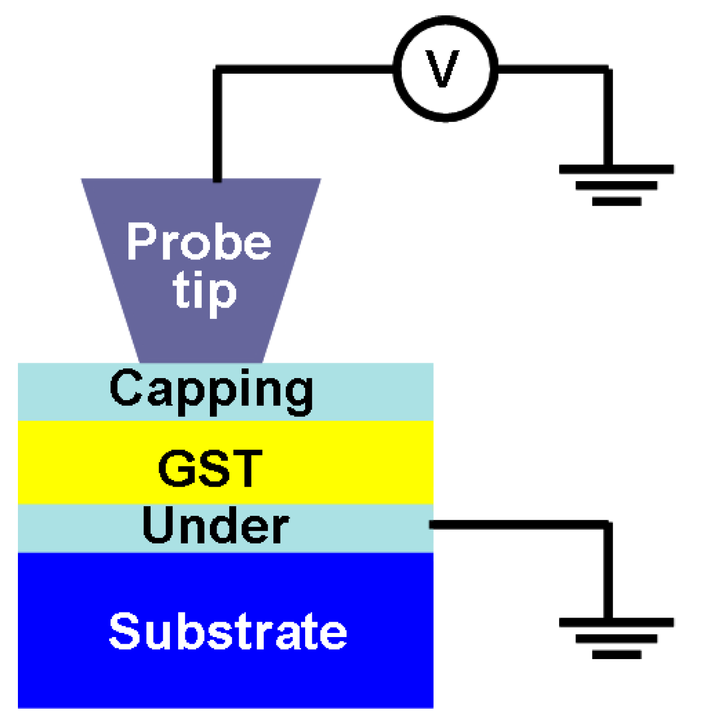
3. Design Approaches Review of Phase-Change Electrical Probe Memory
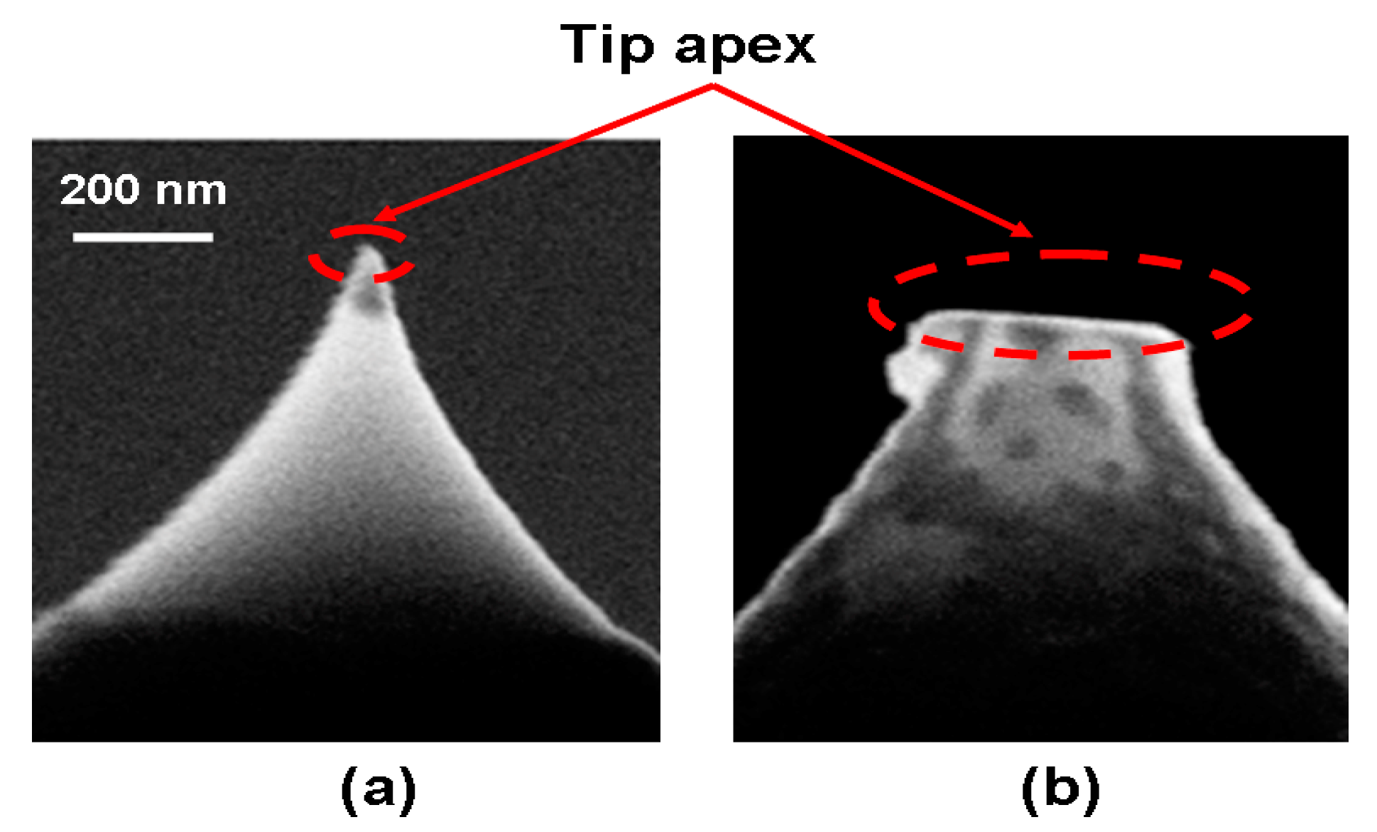
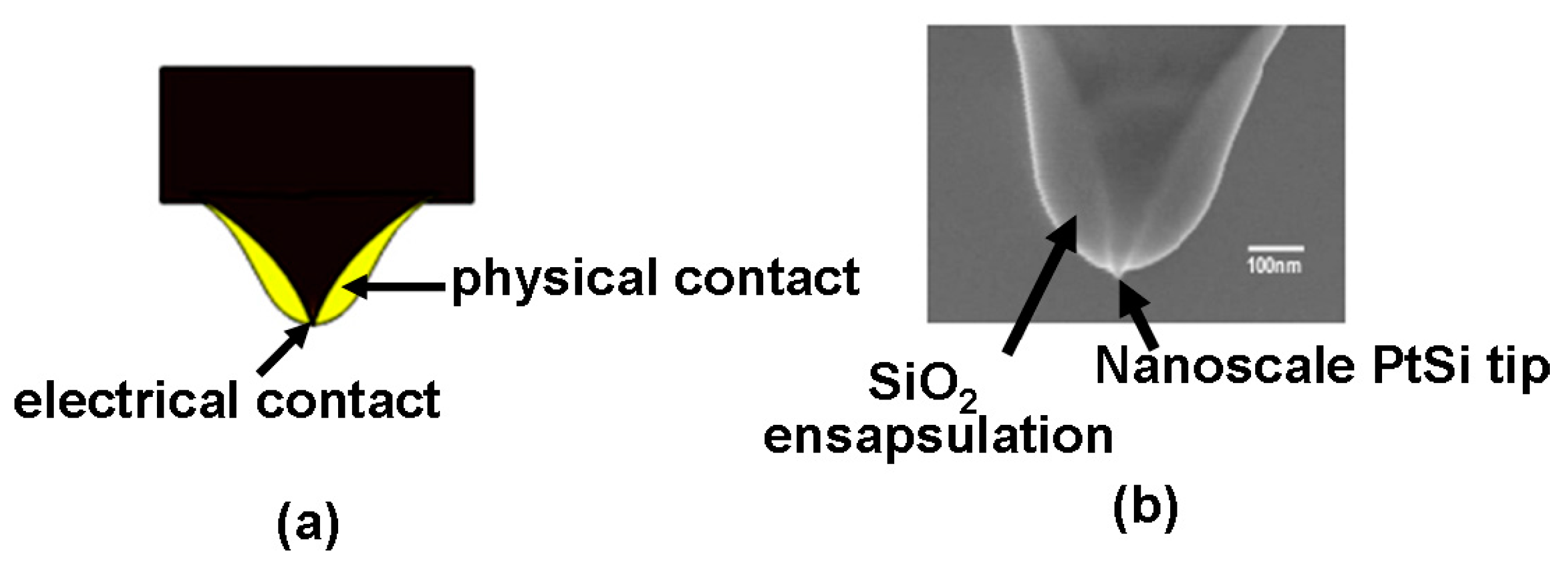
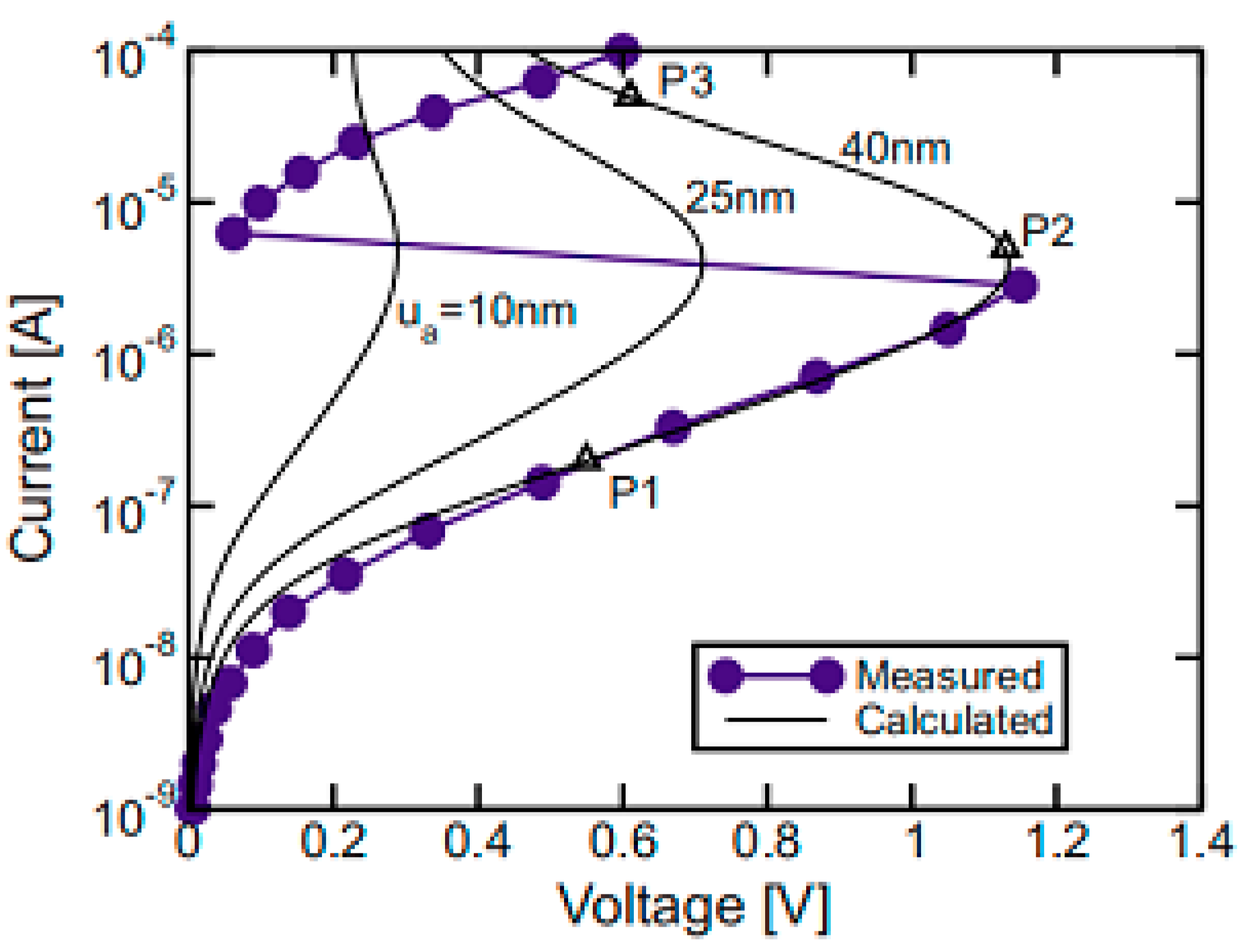
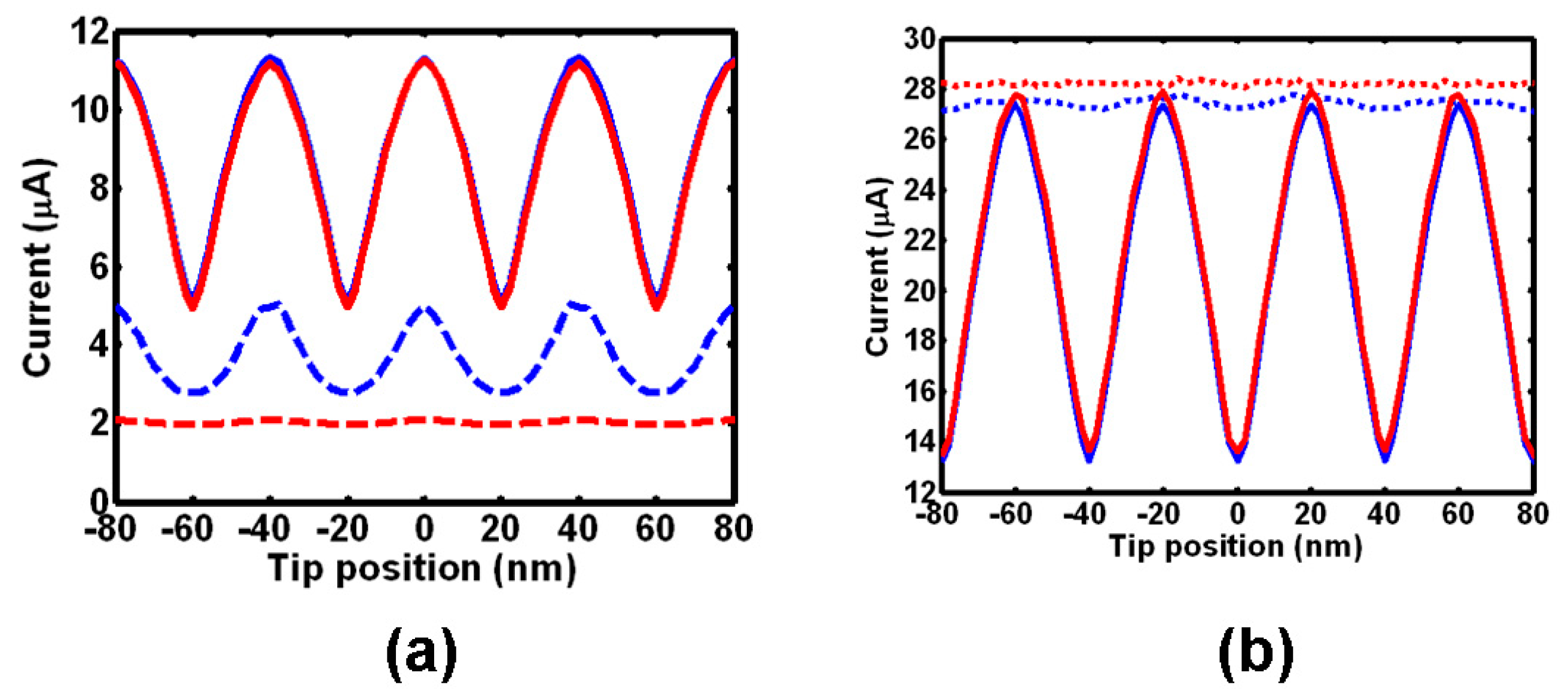
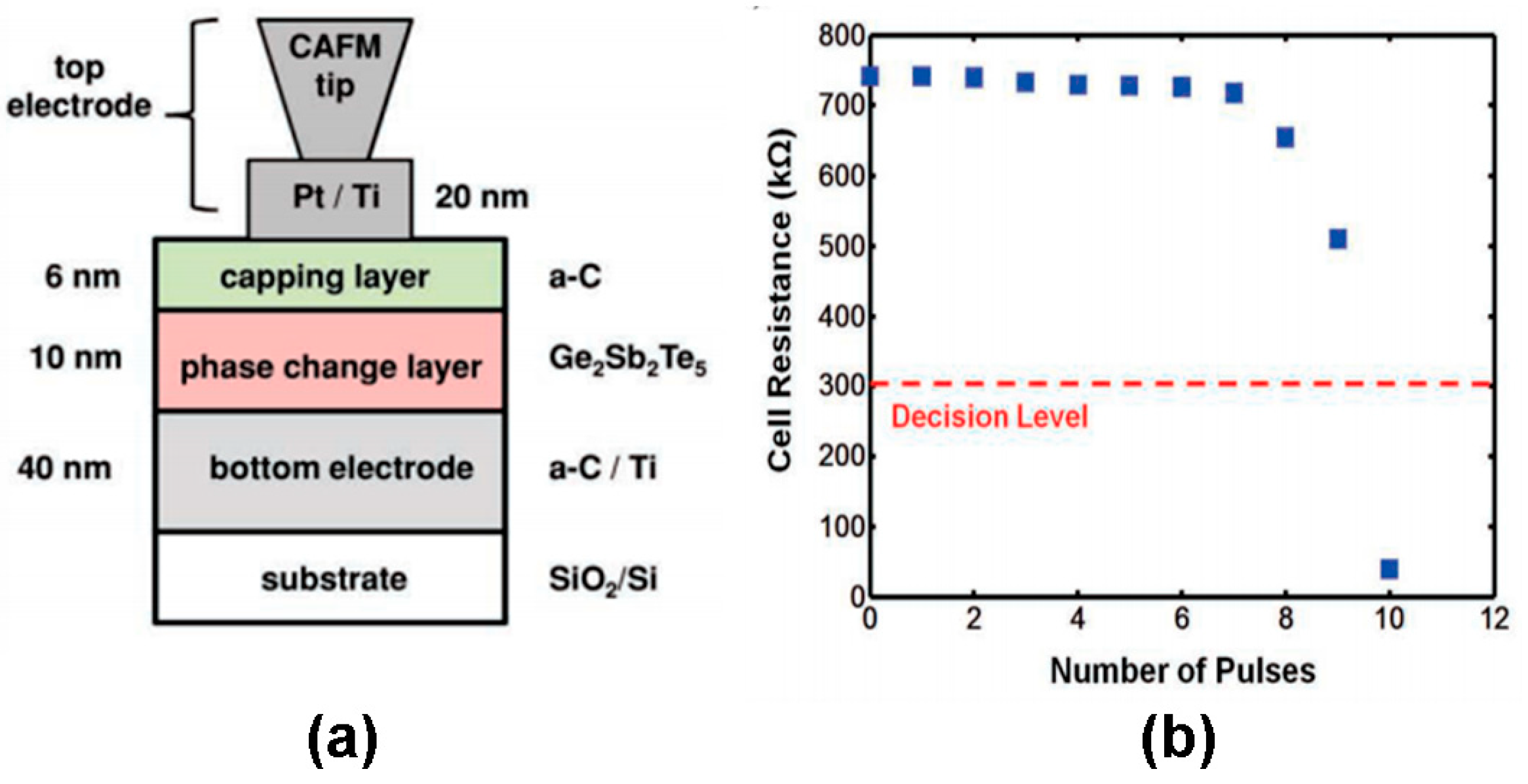
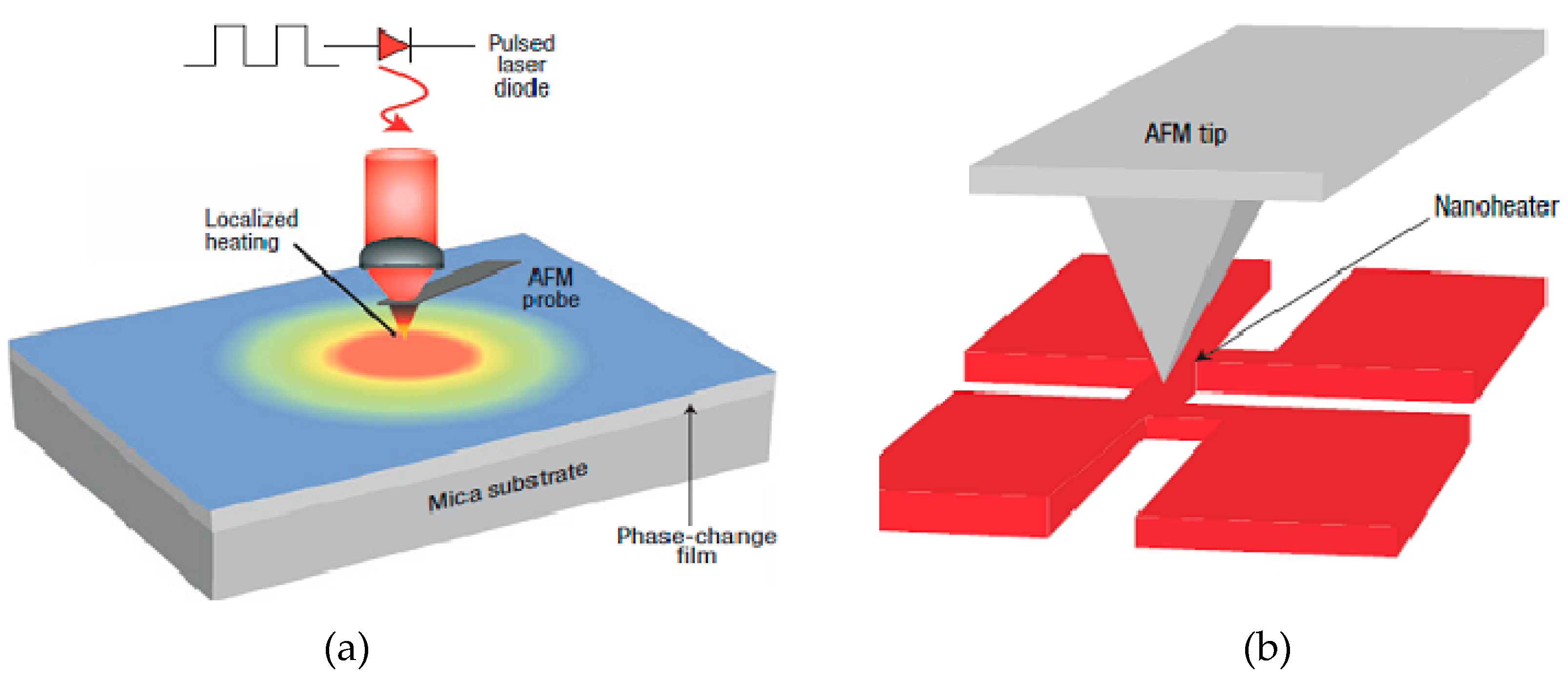
3.1. Role of Probe Tip
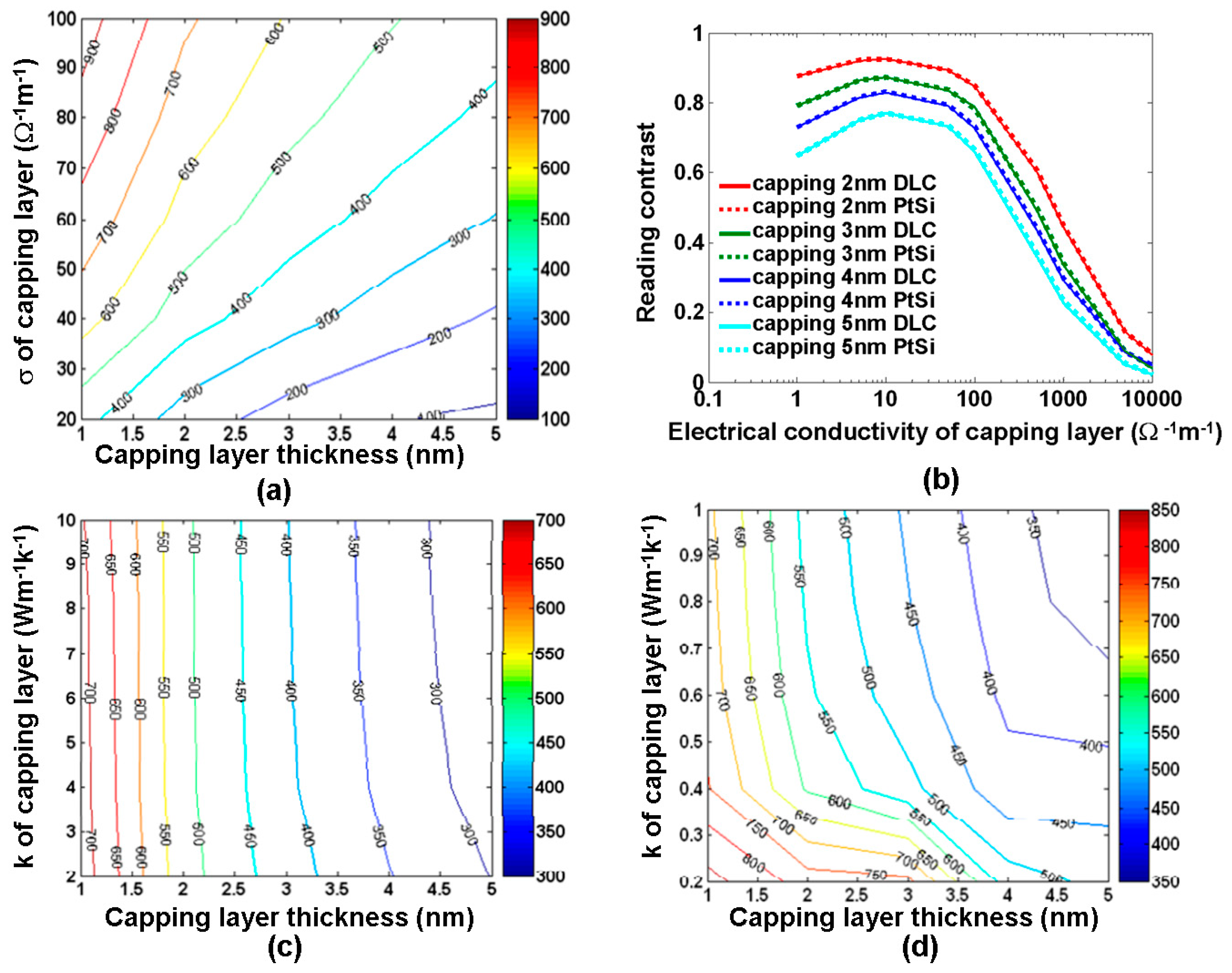
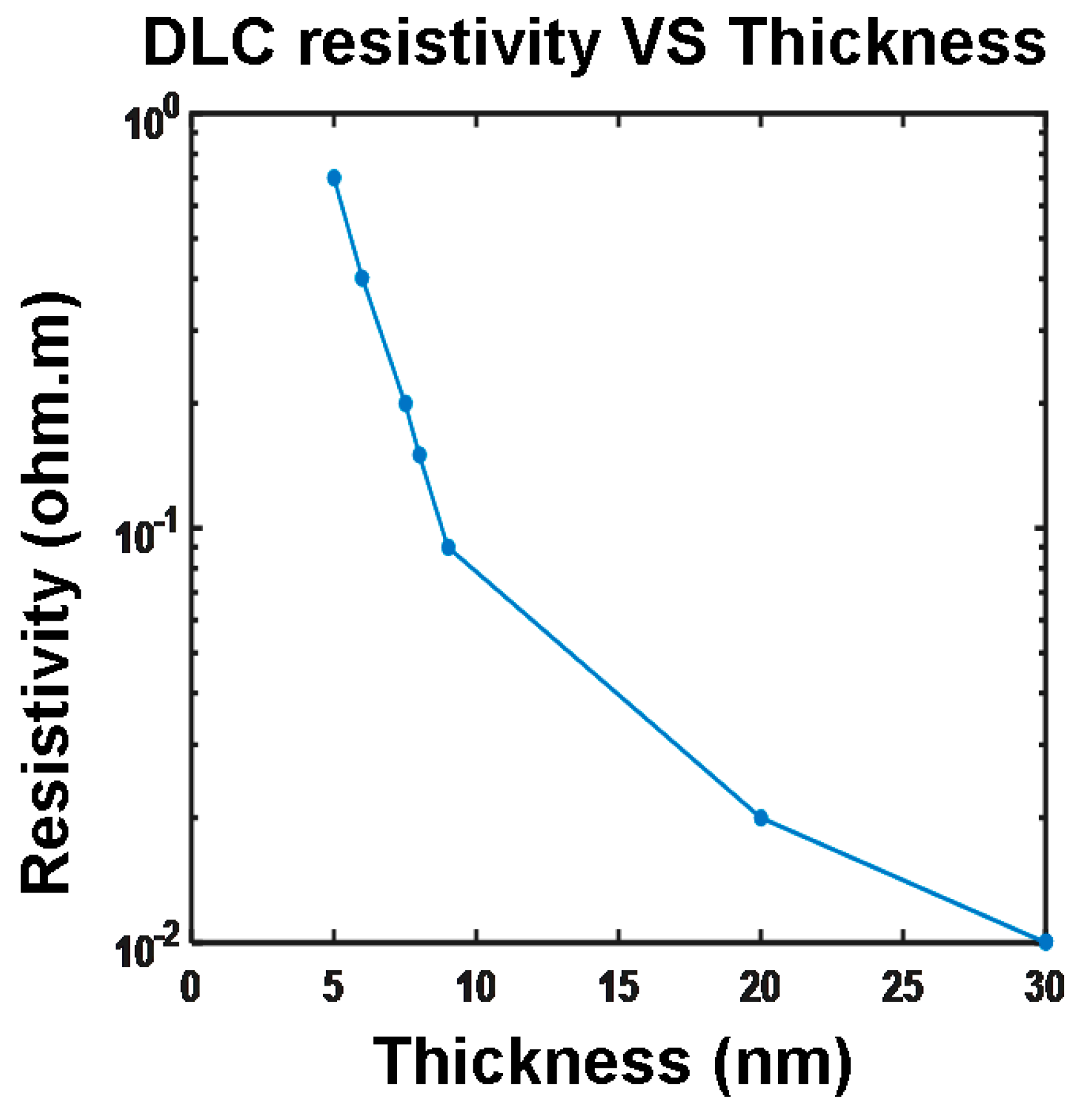
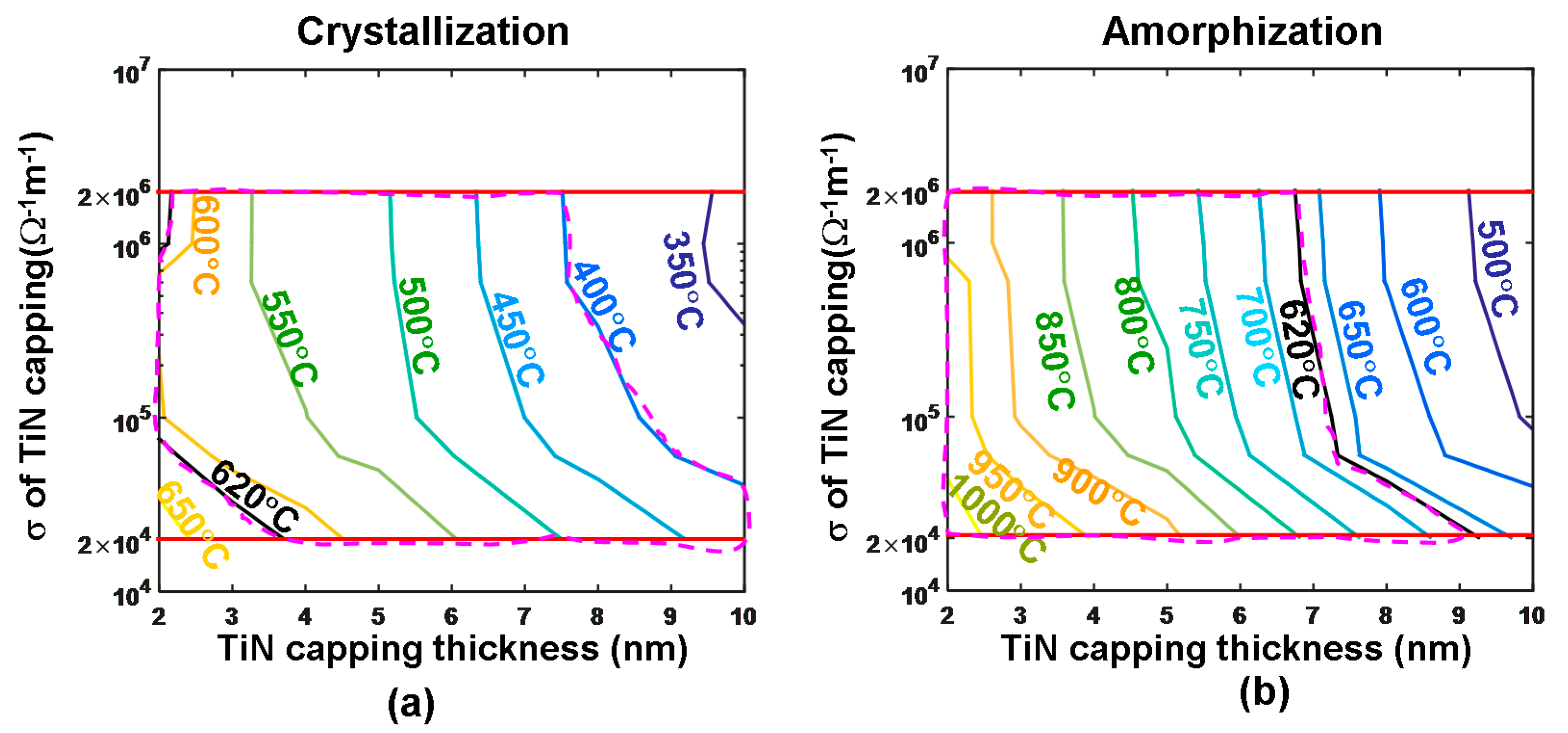
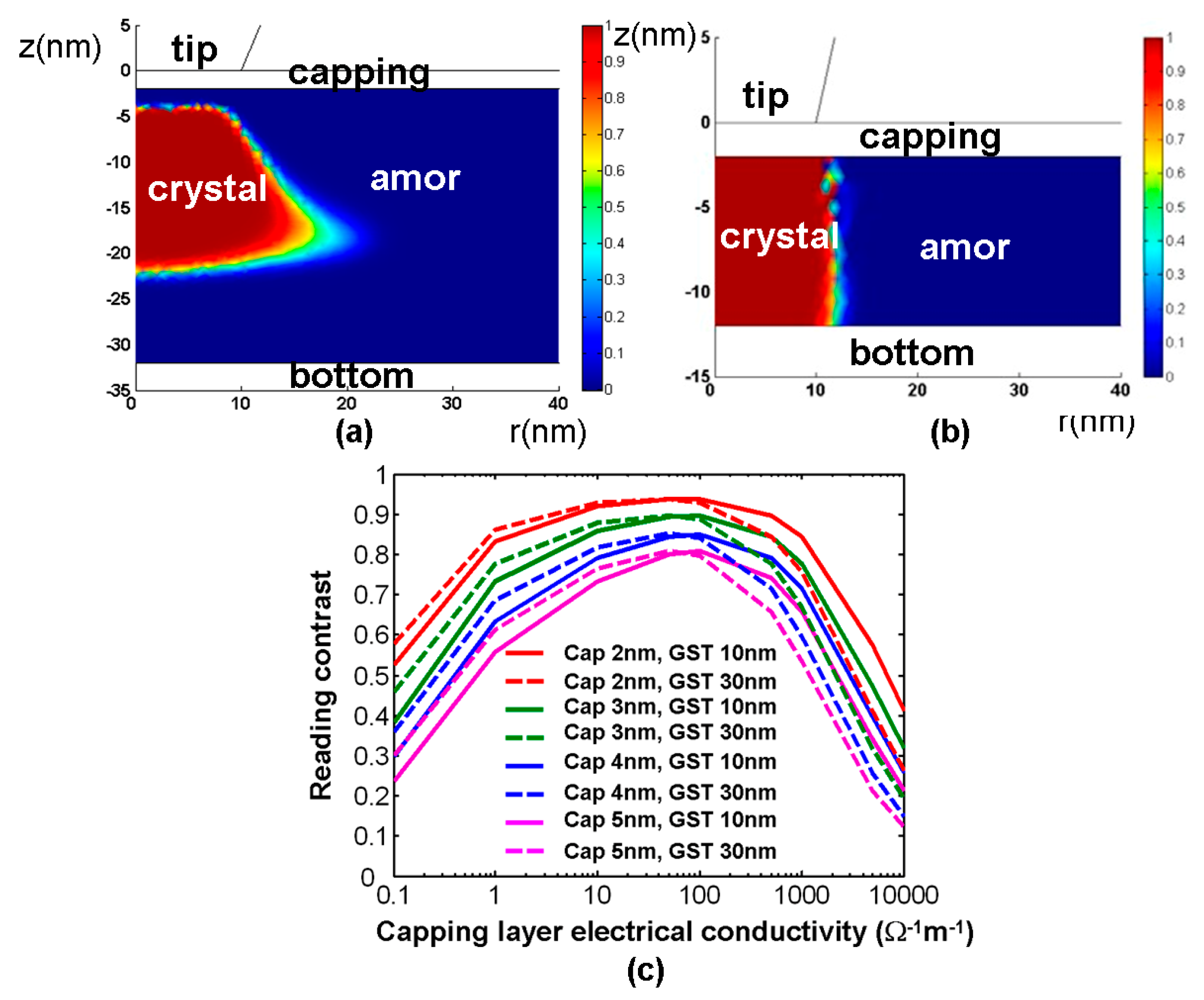
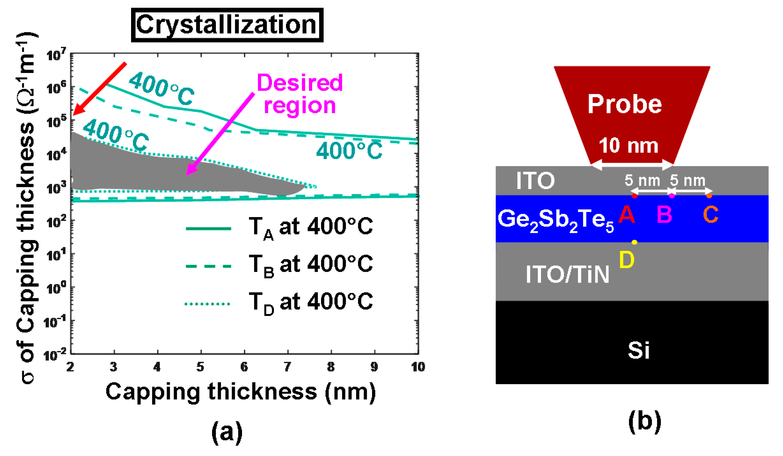
3.2. Role of Capping Layer
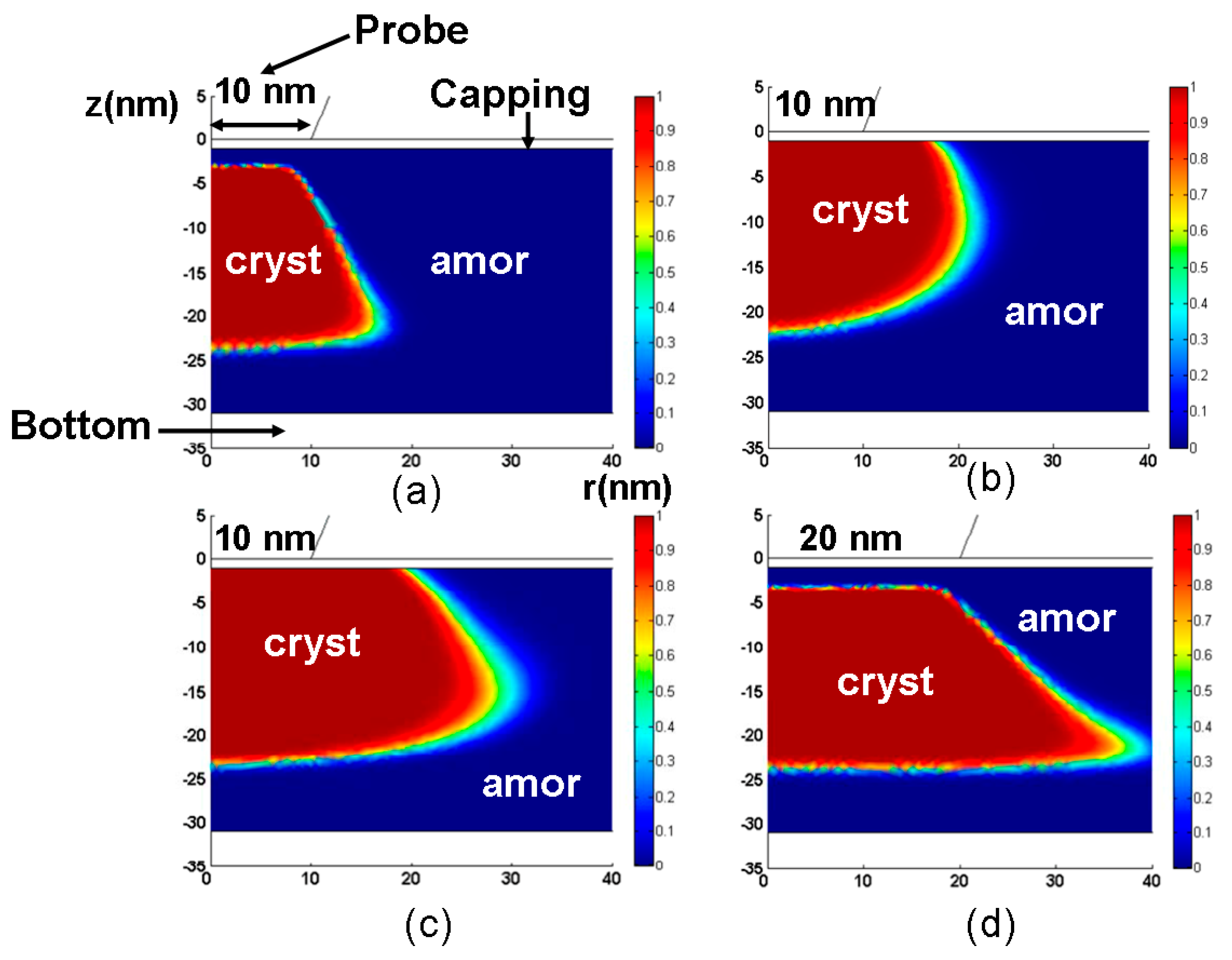
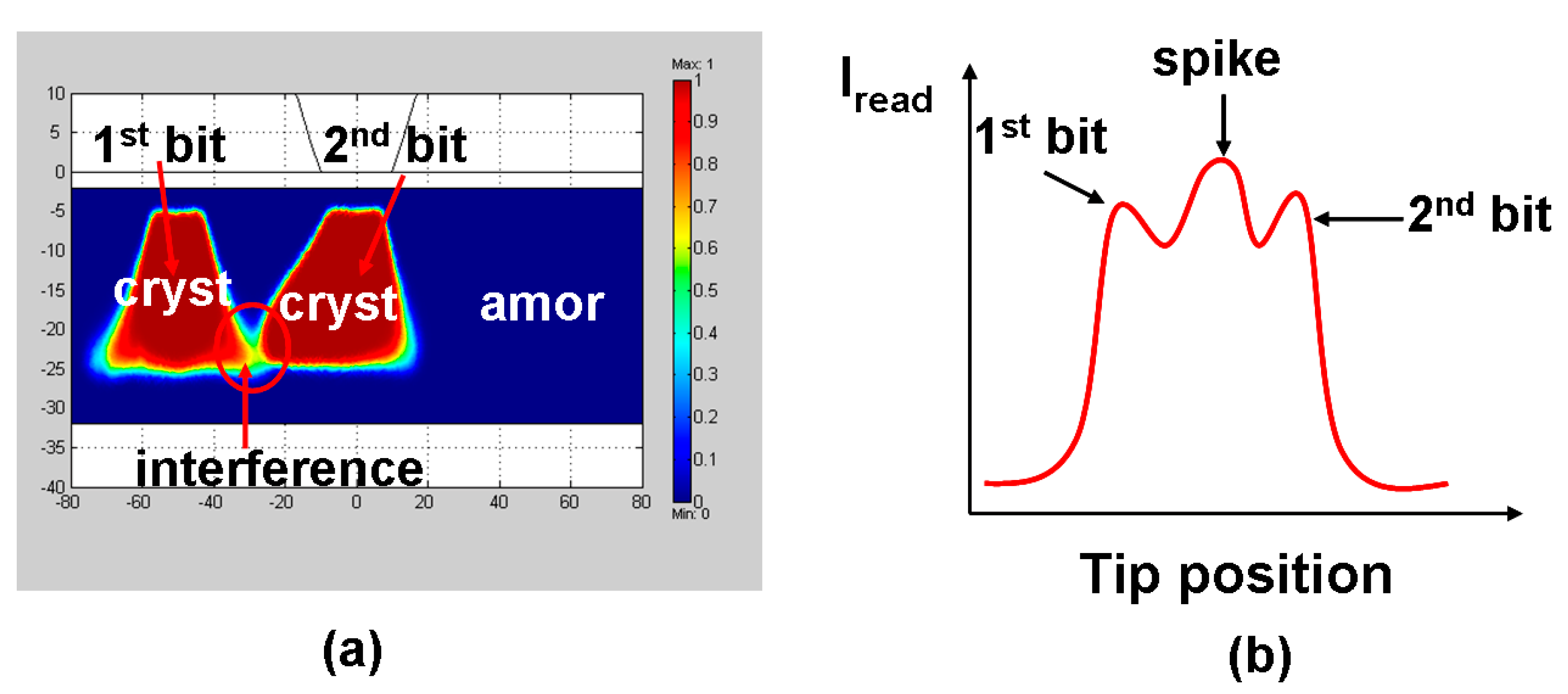
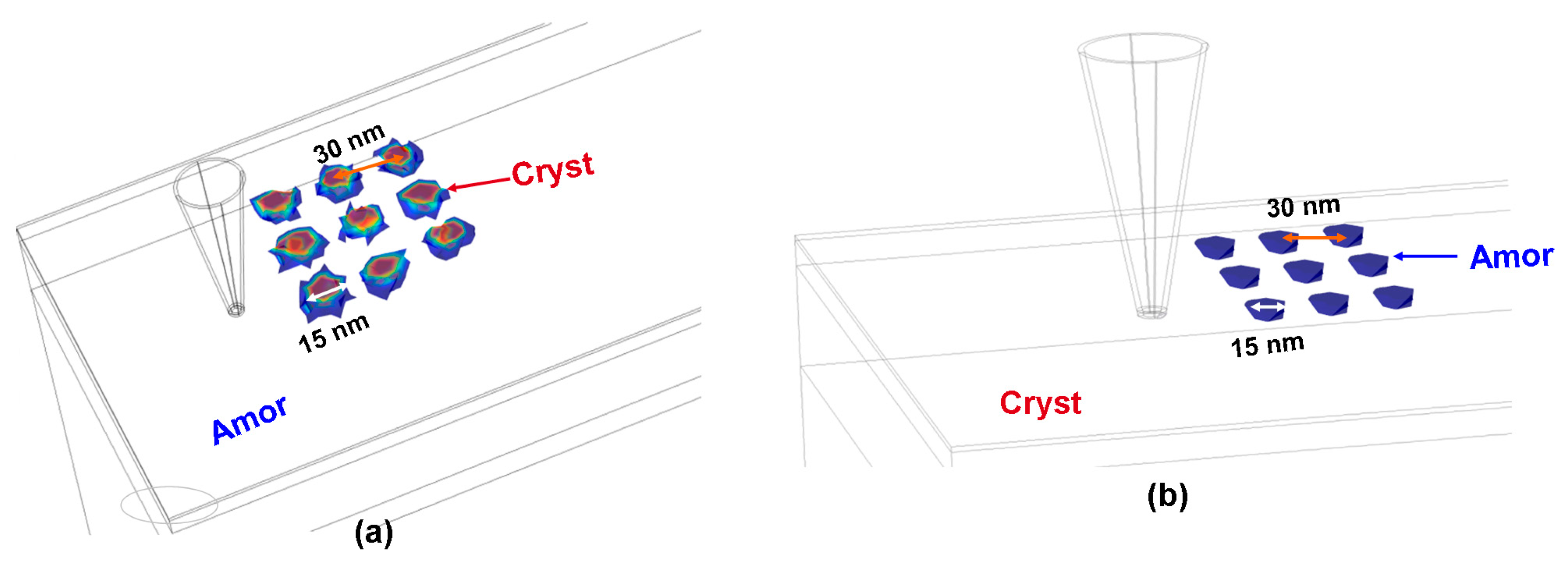
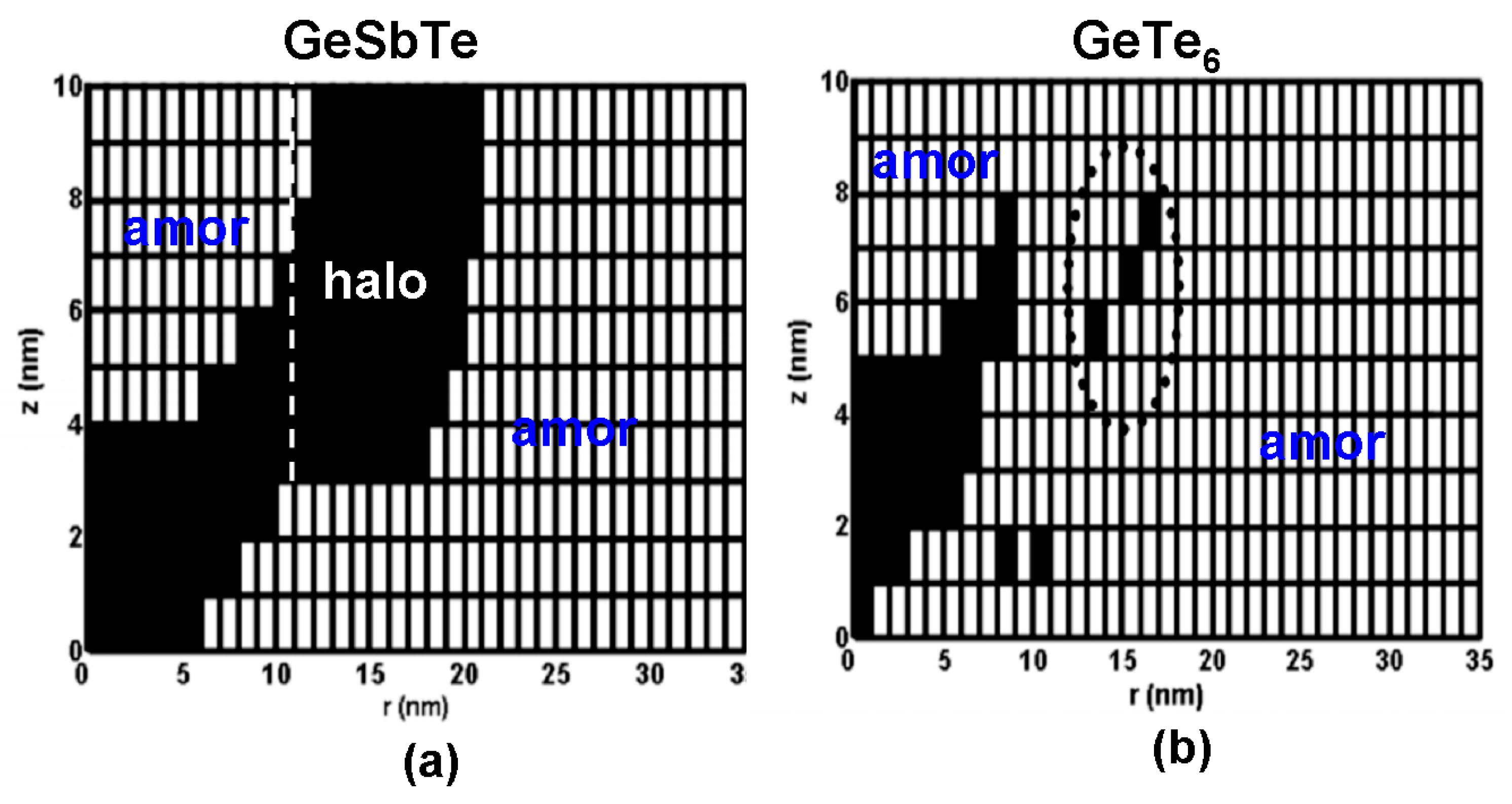
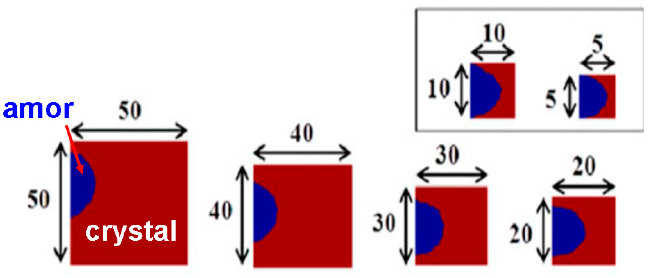
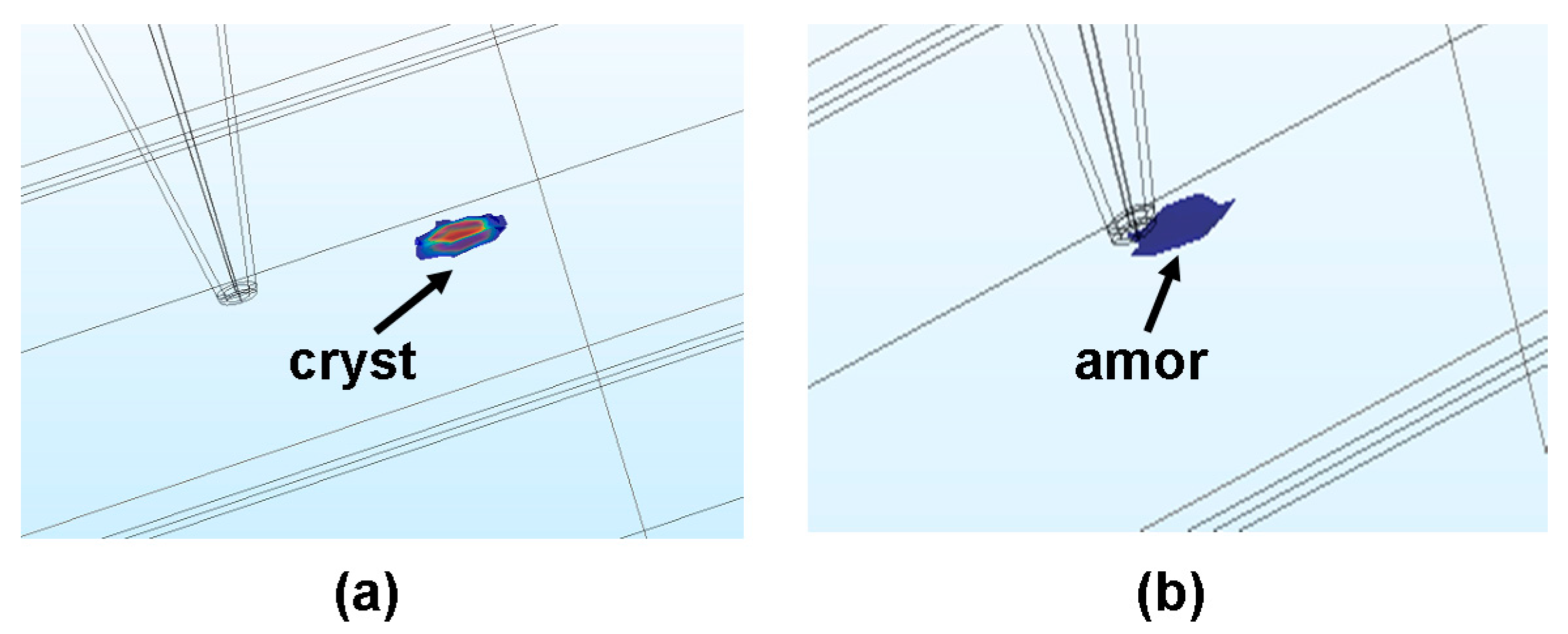
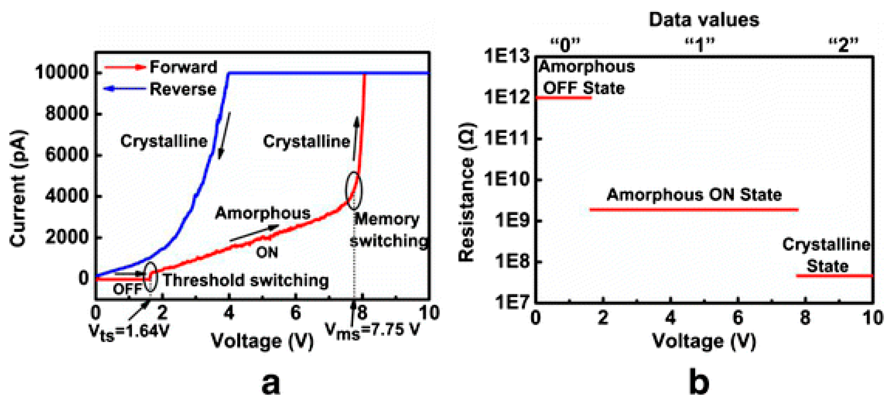
3.3. Role of the Storage Layer
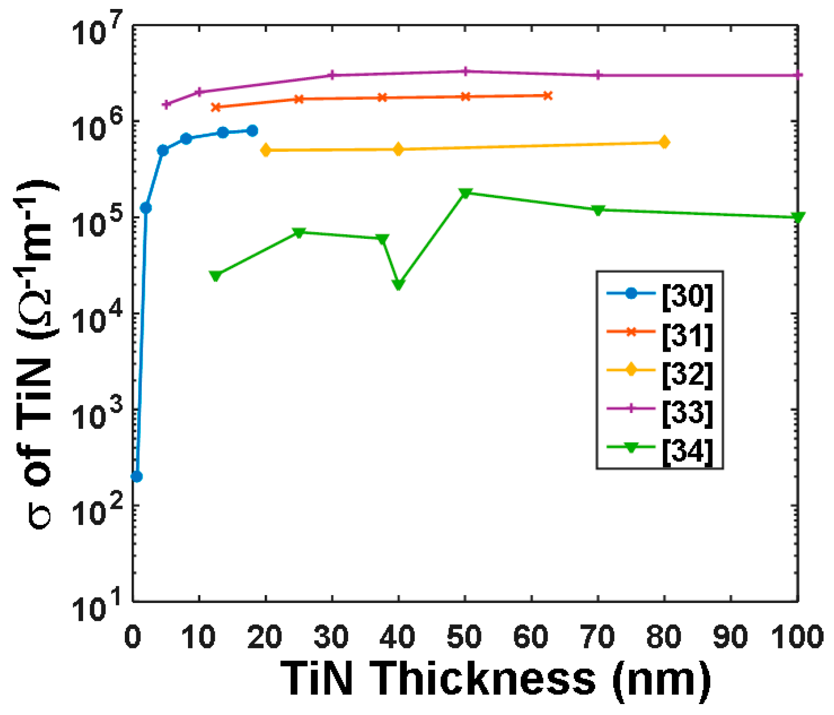
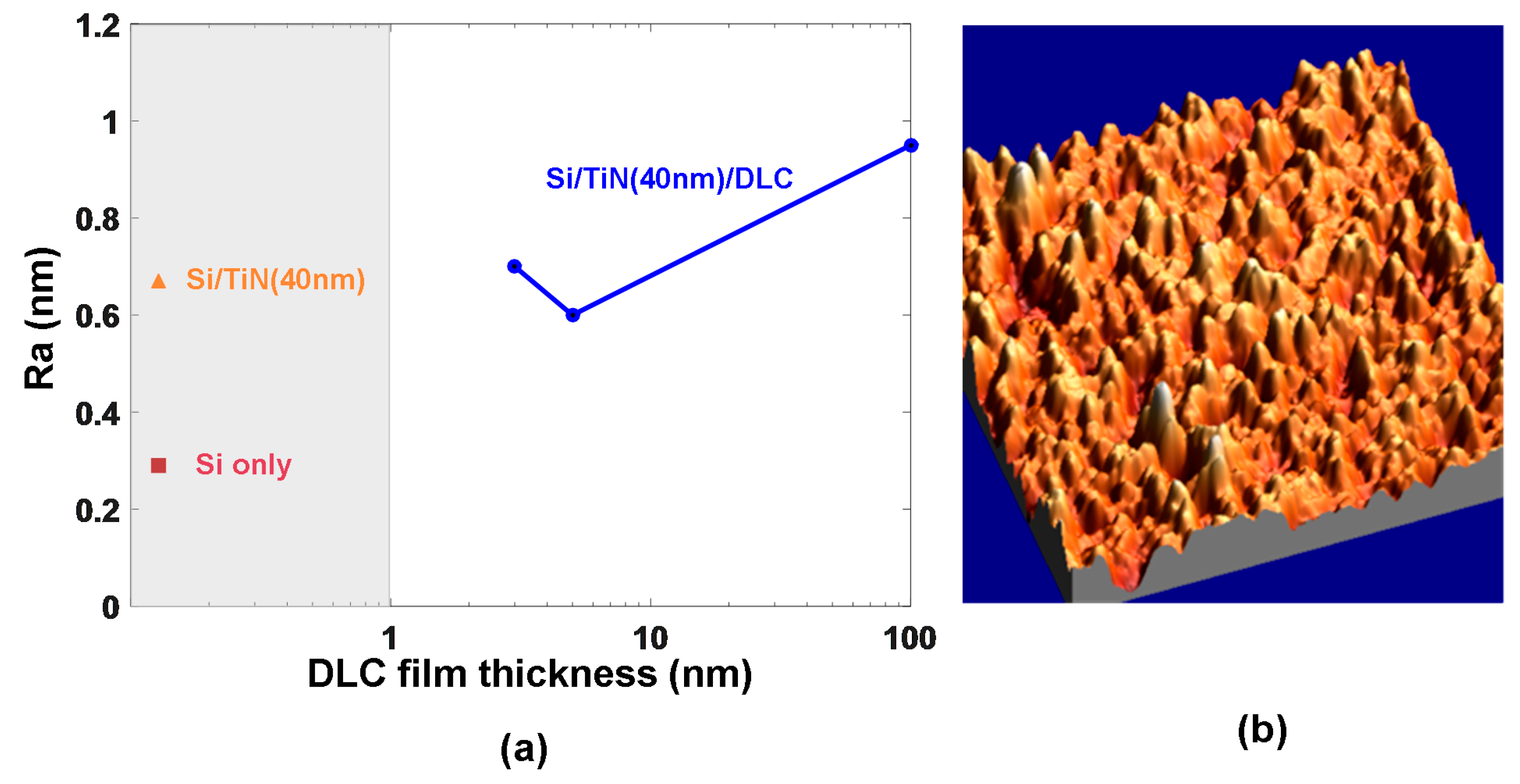
3.4. Role of the Bottom Layer
4. Current status of Phase-Change Electrical Probe Memory
4.1. Recent Progress on Phase-Change Electrical Probe Memory from Authors’ Group
4.2. Recent Progress on Phase-Change Electrical Probe Memory from Other Groups
5. Conclusions
Author Contributions
Funding
Conflicts of Interest
References
- Iwasaki, S. Perpendicular magnetic recording-Its development and realization. J. Magn. Magn. Mater. 2012, 324, 244–247. [Google Scholar] [CrossRef]
- Koide, D.; Takano, Y.; Tokumaru, H.; Onagi, N.; Aman, Y.; Murata, S.; Sugimoto, Y.; Ohishi, K. High-speed recording up to 15000 rpm using thin optical disks. Jpn. J. Appl. Phys. 2008, 47, 5822–5827. [Google Scholar] [CrossRef]
- Lu, C.Y. Future prospects of NAND Flash memory technology-the evolution from floating gate to charge trapping to 3D stacking. J. Nanosci. Nanotechnol. 2012, 85, 7604–7618. [Google Scholar] [CrossRef]
- Chang, K.-C.; Chang, T.-C.; Tsai, T.-M.; Zhang, R.; Hung, Y.-C.; Syu, Y.-E.; Chang, Y.-F.; Chen, M.-C.; Chu, T.-J.; Chen, H.-L.; et al. Physical and chemical mechanisms in oxide-based resistance random access memory. Nanoscale Res. Lett. 2015, 10, 120–146. [Google Scholar] [CrossRef] [PubMed]
- Mansuripur, M. DNA, Human Memory, and the storage technology of the 21st century. Proc. SPIE 2001, 4342, 1–29. [Google Scholar] [CrossRef]
- Gleeson, M.R.; Liu, S.; Sheridan, J.T. The production of primary radical in photopolymers during holographic exposure. Optik 2010, 121, 2273–2275. [Google Scholar] [CrossRef]
- Wright, C.D.; Marilyn, M.; Aziz, M.M. Terabit-per-square-inch data storage using phase-change media and scanning electrical nanoprobes. IEEE Trans. Nanotechnol. 2006, 5, 50–61. [Google Scholar] [CrossRef] [Green Version]
- Vettiger, P.; Cross, G.; Despont, M.; Drechsler, U.; Durig, U.; Gotsmann, B.; Haberle, W.; Lantz, M.A.; Rothuizen, H.E.; Stutz, R.; et al. The millipede-Nanotechnology entering data storage. IEEE Trans. Nanotechnol. 2002, 99, 39–54. [Google Scholar] [CrossRef]
- Onoue, T.; Siekman, M.; Abelmann, L.; Lodder, J.C. Probe recording on CoNi/Pt multilayered thin films by using an MFM tip. J. Magn. Magn. 2004, 272, 2317–2318. [Google Scholar] [CrossRef]
- Cho, Y.; Hashimoto, S.; Odagawa, N.; Tanaka, K.; Hiranaga, Y. Nanodomain manipulation for ultrahigh density ferroelectric data storage. Nanotechnology 2006, 17, S137–S141. [Google Scholar] [CrossRef] [PubMed]
- Jo, A.; Joo, W.; Jin, W.-H.; Nam, H.; Kim, J.K. Ultrahigh-density phase-change data storage without the use of heating. Nat. Nanotechnol. 2009, 4, 727–731. [Google Scholar] [CrossRef] [PubMed]
- Simpson, R.E.; Krbal, M.; Fons, P.; Kolobov, A.V.; Tominaga, J.; Uruga, T.; Tanida, H. Toward the ultimate limit of phase-change in Ge2Sb2Te5. Nano Lett. 2009, 10, 414–419. [Google Scholar] [CrossRef] [PubMed]
- Wuttig, M.; Yamada, N. Phase-change materials for rewritable data storage. Nat. Mater. 2007, 6, 824–832. [Google Scholar] [CrossRef] [PubMed]
- Russo, U.; Ielmini, D.; Redaelli, A.; Lacaita, A.L. Intrinsic data retention in nanoscaled phase-change memories-Part I: Monte Carlo model for crystallization and percolation. IEEE Trans. Electron. Dev. 2006, 53, 3032–3039. [Google Scholar] [CrossRef]
- Lacaita, A.L.; Wouters, D.J. Phase-change memories. Phys. Stat. Sol. 2008, 205, 2281–2297. [Google Scholar] [CrossRef]
- Kado, H.; Tohda, T. Nanometer-scale erasable recording using atomic force microscope on phase change media. Jpn. J. Appl. Phys. 1997, 36, 523–525. [Google Scholar] [CrossRef]
- Gotoh, T.; Sugawara, K.; Tanaka, K. Nanoscale electrical phase-change in GeSb2Te4 films with scanning probe microscopes. J. Non-Cryst. Solids 2002, 299–302, 968–972. [Google Scholar] [CrossRef]
- Satoh, H.; Sugawara, K.; Tanaka, K. Nanoscale phase changes in crystalline Ge2Sb2Te5 films using scanning probe microscopes. J. Appl. Phys. 2006, 99, 024306–024307. [Google Scholar] [CrossRef]
- Tanaka, K. Smallest (~10 nm) phase-change marks in amorphous and crystalline Ge2Sb2Te5 films. J. Non-Cryst. Solids 2007, 353, 1899–1903. [Google Scholar] [CrossRef]
- Pandian, R.; Kooi, B.J.; Palasantzas, G.; De Hosson, J.T.M.; Pauza, A. Nanoscale electrolytic switching of in phase-change chalcogenide films. Adv. Mater. 2007, 19, 4431–4437. [Google Scholar] [CrossRef]
- Sun, X.; Rob, U.; Gerlach, J.W.; Lotnyk, A.; Rauschenbach, B. Nanoscale bipolar switching of Ge2Sb2Te5 phase-change material thin films. Adv. Electron. Mater. 2017, 3, 1700283. [Google Scholar] [CrossRef]
- Manivannan, A.; Myana, S.K.; Miriyala, K.; Sahu, S.; Ramadurai, R. Low power ovonic threshold switching characteristics of thin GeTe6 films using conductive atomic force microscopy. Appl. Phys. Lett. 2014, 105, 243501–243505. [Google Scholar] [CrossRef]
- Bhaskaran, H.; Sebastian, A.; Despont, M. Nanoscale PtSi tips for conducting probe technologies. IEEE Trans. Nanotechnol. 2009, 8, 128–131. [Google Scholar] [CrossRef]
- Bhaskaran, H.; Sebastian, A.; Drechsler, U.; Despont, M. Encapsulated tip for reliable nanoscale conduction in scanning probe technologies. Nanotechnology 2009, 20, 105701–105708. [Google Scholar] [CrossRef] [PubMed]
- Robertson, J. Diamond like amorphous carbon. Mater. Sci. Eng. R 2002, 37, 129–281. [Google Scholar] [CrossRef]
- Wang, L.; Wen, J.; Yang, C.; Gai, S.; Miao, X.S. Optimisation of write performance of pahse-change probe memory for future storage applications. Nanosci. Nanotechnol. Lett. 2015, 7, 870–878. [Google Scholar] [CrossRef]
- Wang, L.; Wright, C.D.; Aziz, M.M.; Yang, C.; Yang, G.W. Optimisation of readout performance of phase-change probe memory in terms of capping layer and probe tip. Electron. Mater. Lett. 2014, 10, 1045–1049. [Google Scholar] [CrossRef]
- Wang, L.; Wright, C.D.; Aziz, M.M.; Ying, J.; Yang, G.W. Optimisation of scanning probe phase-change memory in terms of the thermal conductivities of capping and under layer. EPL 2013, 104, 56007. [Google Scholar] [CrossRef]
- Wang, L.; Gong, S.D.; Yang, C.H.; Wen, J. Towards low energy consumption data storage era using phase-change probe memory with TiN bottom electrode. Nanotechnol. Rev. 2016, 5, 455–460. [Google Scholar] [CrossRef]
- Wang, L.; Wright, C.D.; Aziz, M.M.; Ying, J.; Yang, G.W. A contact resistance model for scanning probe phase-change memory. J. Micromech. Microeng. 2014, 24, 037001–037006. [Google Scholar] [CrossRef]
- Van Bui, H.; Kovalgin, A.Y.; Wolters, R.A.M. On the difference between optically and electrically determined resistivity of ultra-thin titanium nitride films. Appl. Surf. Sci. 2013, 269, 45–49. [Google Scholar] [CrossRef]
- Liang, H.L.; Xu, J.; Zhou, D.Y.; Sun, X.; Chu, S.C.; Bai, Y.Z. Thickness dependent microstructural and electical properties of TiN thin films prepared by DC reactive magnetron sputtering. Ceram. Int. 2016, 42, 2642–2647. [Google Scholar] [CrossRef]
- Jeyachandran, Y.L.; Narayandass, S.K.; Mangalaraj, D.; Areva, S.; Mielczarski, J.A. Properties of titanium nitride films prepared by direct current magnetron sputtering. Mater. Sci. Eng. A 2007, 445–446, 223–226. [Google Scholar] [CrossRef]
- Yokota, K.; Nakamura, K.; Kasuya, T.; Mukai, K.; Ohnishi, M. Resistivities of titanium nitride films prepared onto silicon by an ion beam assisted deposition method. J. Phys. D Appl. Phys. 2004, 37, 1095–1101. [Google Scholar] [CrossRef]
- Yang, Z.Y.; Chen, Y.H.; Liao, B.H.; Chen, K.P. Room temperature fabrication of titanium nitride thin films as plasmonic materials by high-power impulse magnetron sputtering. Opt. Mater. Express 2016, 6, 540–551. [Google Scholar] [CrossRef]
- Wang, L.; Wen, J.; Yang, C.; Xiong, B.S. Design of electrical probe memory with TiN capping layer. J. Mater. Sci. 2018, 53, 15549–15558. [Google Scholar] [CrossRef]
- Ielmini, D. Threshold switching mechanism by high-field energy gain in the hopping transport of chalcogenide glasses. Phys. Rev. B 2008, 78, 035308–035317. [Google Scholar] [CrossRef]
- Wang, L.; Wright, C.D.; Aziz, M.M.; Yang, C.H.; Yang, G.W. Design of an optimised readout architecture for phase-change probe memory using Ge2Sb2Te5 media. Jpn. J. Appl. Phys. 2014, 53, 28002–28003. [Google Scholar] [CrossRef]
- Chang, Y.F.; Chen, P.Y.; Chen, Y.T.; Xue, F.; Wang, Y.; Zhou, F.; Fowler, B.; Lee, J.C. Study of polarity effect in SiOx-based resistive switching memory. Appl. Phys. Lett. 2012, 101, 052111–052113. [Google Scholar] [CrossRef]
- Park, J.; Kim, S.W.; Kim, J.H.; Ko, D.H.; Wu, Z. Phase change memory employing a Ti diffusion barrier for reducing reset current. Thin Solid Films 2016, 612, 135–140. [Google Scholar] [CrossRef]
- Guo, E.-J.; Guo, H.Z.; Lu, H.B.; Jin, K.J.; He, M.; Yang, G.Z. Structure and characteristics of ultrathin indium tin oxide films. Appl. Phys. Lett. 2011, 98, 011905–011907. [Google Scholar] [CrossRef]
- Brinzari, V.I.; Cocemasov, A.I.; Nika, D.L.; Korotcenkov, G.S. Ultra-low thermal conductivity of nanogranular indium tin oxide films deposited by spray pyrolysis. Appl. Phys. Lett. 2017, 110, 071904–071908. [Google Scholar] [CrossRef]
- Liu, D.-S.; Sheu, C.-S.; Lee, C.-T.; Lin, C.-H. Thermal stabilit of indium tin oxide thin films co-sputtered with zinc oxide. Thin Solid Films 2008, 516, 3196–3203. [Google Scholar] [CrossRef]
- Gidon, S.; Lemonnier, O.; Rolland, B.; Bichet, O.; Dressler, C. Electrical probe storage using joule heating in phase change media. Appl. Phys. Lett. 2004, 85, 6392–6394. [Google Scholar] [CrossRef]
- Kim, H.H.; Choi, S.K.; Kang, S.H.; Oh, K.H. Structural phase transitions of Ge2Sb2Te5 cells with TiN electrodes using a homemade W heater tip. Appl. Phys. Lett. 2007, 90, 083103–083106. [Google Scholar] [CrossRef]
- Bhaskaran, H.; Sebastian, A.; Pauza, A.; Pozidis, H.; Despont, M. Nanoscale phase transformation in Ge2Sb2Te5 using encapsulated scanning probes and retraction force microscopy. Rev. Sci. Instrum. 2009, 80, 083701. [Google Scholar] [CrossRef] [PubMed]
- Wright, C.D.; Wang, L.; Shah, P.; Aziz, M.M.; Varesi, E.; Bez, R.; Moroni, M.; Cazzaniga, F. The design of rewritable ultrahigh density scanning-probe phase-change memories. IEEE Trans. Nanotechnol. 2011, 10, 900–912. [Google Scholar] [CrossRef]
- Wang, L.; Wen, J.; Yang, C.; Gai, S.; Peng, Y. The route for ultra-high recording density using probe-based data storage device. Nano 2015, 8, 1550118. [Google Scholar] [CrossRef]
- Wang, L.; Wright, C.D.; Aziz, M.M.; Ying, J.; Yang, G.W. A physics-based three dimensional model for write and read performances of phase-change probe memory. J. Nanosci. Nanotechnol. 2015, 15, 2785–2789. [Google Scholar] [CrossRef] [PubMed]
- Wang, L.; Yang, C.; Wen, J.; Xiong, B.S. Amorphization optimization of Ge2Sb2Te5 media for electrical probe memory applications. Nanomaterials 2018, 8, 368. [Google Scholar] [CrossRef] [PubMed]
- Hayat, H.; Kohary, K.; Wright, C.D. Ultrahigh storage densities via the scaling of patterned probe phase-change memories. IEEE Trans. Nanotechnol. 2017, 16, 767–772. [Google Scholar] [CrossRef]
- Yang, F.; Xu, L.; Chen, J.; Xu, J.; Yu, Y.; Ma, Z.-Y.; Chen, K.J. Nanoscale multilevel switching in Ge2Sb2Te5 thin film with conductive atomic force microscopy. Nanotechnology 2016, 27, 035706–035707. [Google Scholar] [CrossRef] [PubMed]
- Wright, C.D.; Hosseini, P.; Vazquez Diosdado, J.A. Beyond von-Neumann computing with nanoscale phase-change memory devices. Adv. Funct. Mater. 2013, 23, 2248–2254. [Google Scholar] [CrossRef] [Green Version]
- Hamann, H.F.; O’Boyle, M.; Martin, Y.C.; Rooks, M.; Wickramasinghe, H.K. Ultra-high-density phase-change storage and memory. Nat. Mater. 2006, 5, 383–387. [Google Scholar] [CrossRef] [PubMed]
- Wang, L.; Pan, J.; Wen, J. The exploration of role of tip-sample contact on scanning probe phase-change memory. Mater. Lett. 2017, 206, 169–171. [Google Scholar] [CrossRef]


| Group | Storage Mechanism | Architecture | Bit Size (nm) | References |
|---|---|---|---|---|
| Kado | Electrical switch | GeSb2Te4 film Pt electrode | 10–70 | [16] |
| Tanaka | Structural switch | Ge2Sb2Te5 film Pt electrode | 10–100 | [18,19] |
| Pandian | Electrical & structural switch | Ge2Sb2Te5 film Mo electrode | ~100 | [20] |
| Sun | Electrical & structural switch | Ge2Sb2Te5 film Cr electrode | 25–50 | [21] |
| Maniva | Structural switch | GeTe6 film Ag electrode | 300–1000 | [22] |
| Group | Architecture | Capping Property | GST Thickness (nm) | Bottom Property | Bit Image |
|---|---|---|---|---|---|
| Gidon | DLC/GST/DLC | σ: 10 Ω−1·m−1 L: 2 nm k: N/A | 10 | σ: 100 Ω−1·m−1 L: 10 nm k: N/A | 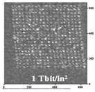 |
| Kim | TiN/GST/TiN | σ: N/A L: 100 nm k: N/A | 20 | σ: N/A L: 100 nm k: N/A | 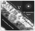 |
| Bhaskaran | N2 doped DLC/GST/N2 doped DLC | σ: 166 Ω−1·m−1 L: 6 nm k: N/A | 20 | σ: 103 Ω−1·m−1 L: 120 nm k: N/A |  |
| Wright | DLC/GST/DLC | σ: 50 Ω−1·m−1 L: 30 nm k: 100·W·m−1·K−1 | 30 | σ: 100 Ω−1·m−1 L: 10 nm k:100 W·m−1·K−1 |  |
| Wang | TiN/GST/DLC | σ: 50 Ω−1·m−1 L: 10 nm k: 0.5 W·m−1·K−1 | 10 | σ: 5 × 10⁶ Ω−1·m−1 L: 40 nm k: 12 W·m−1·K−1 |  |
| Wang | TiN/GST/TiN | σ: 2 × 10⁵ Ω−1·m−1 L: 2 nm k: 12 W·m−1·K−1 | 2 | σ: 5 × 10⁶ Ω−1·m−1 L: 40 nm k: 12 W·m−1·K−1 |  |
© 2018 by the authors. Licensee MDPI, Basel, Switzerland. This article is an open access article distributed under the terms and conditions of the Creative Commons Attribution (CC BY) license (http://creativecommons.org/licenses/by/4.0/).
Share and Cite
Wang, L.; Ren, W.; Wen, J.; Xiong, B. Overview of Phase-Change Electrical Probe Memory. Nanomaterials 2018, 8, 772. https://doi.org/10.3390/nano8100772
Wang L, Ren W, Wen J, Xiong B. Overview of Phase-Change Electrical Probe Memory. Nanomaterials. 2018; 8(10):772. https://doi.org/10.3390/nano8100772
Chicago/Turabian StyleWang, Lei, Wang Ren, Jing Wen, and Bangshu Xiong. 2018. "Overview of Phase-Change Electrical Probe Memory" Nanomaterials 8, no. 10: 772. https://doi.org/10.3390/nano8100772
APA StyleWang, L., Ren, W., Wen, J., & Xiong, B. (2018). Overview of Phase-Change Electrical Probe Memory. Nanomaterials, 8(10), 772. https://doi.org/10.3390/nano8100772