The Advent of Indium Selenide: Synthesis, Electronic Properties, Ambient Stability and Applications


 ,
, 
Abstract
:1. Introduction
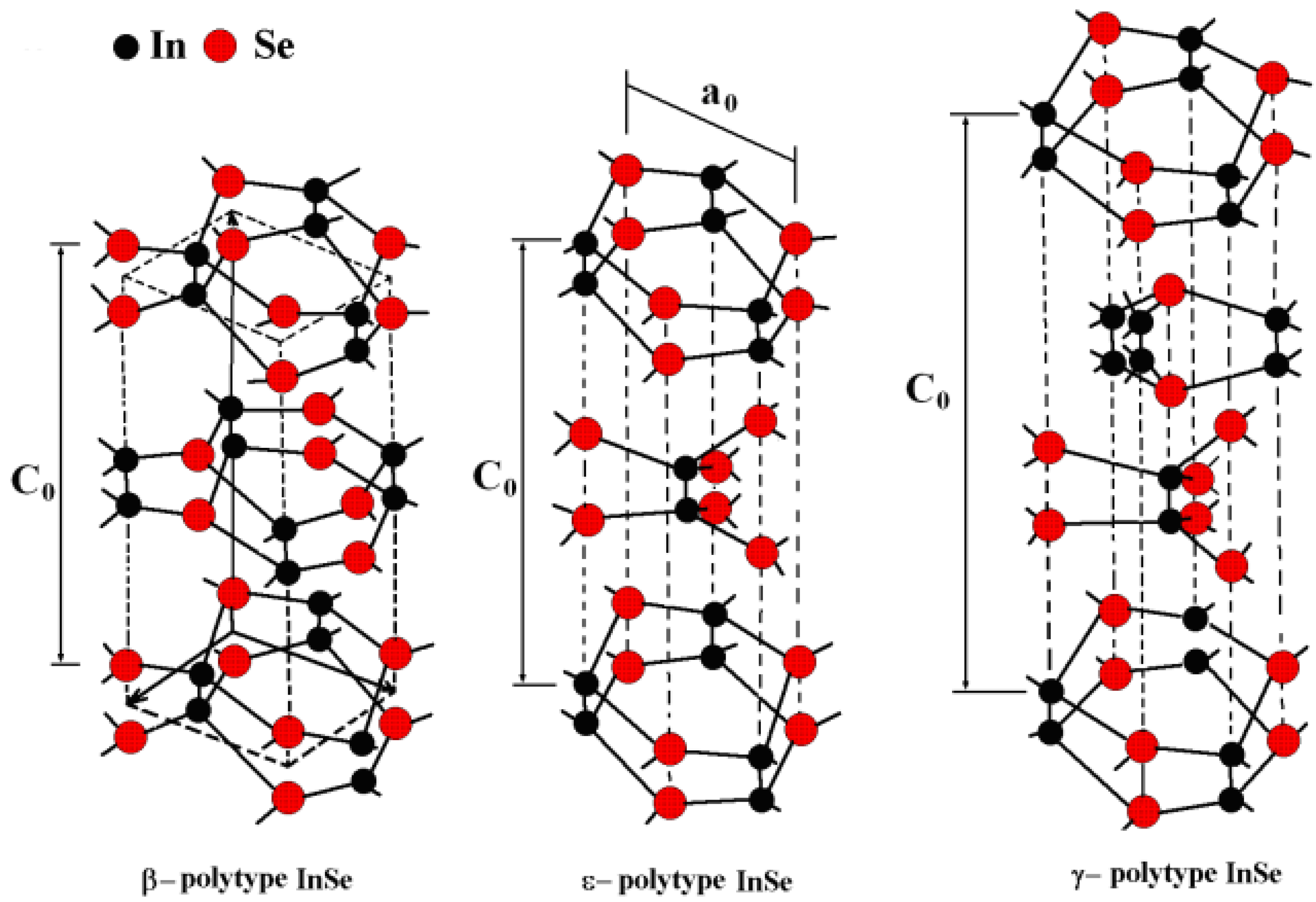
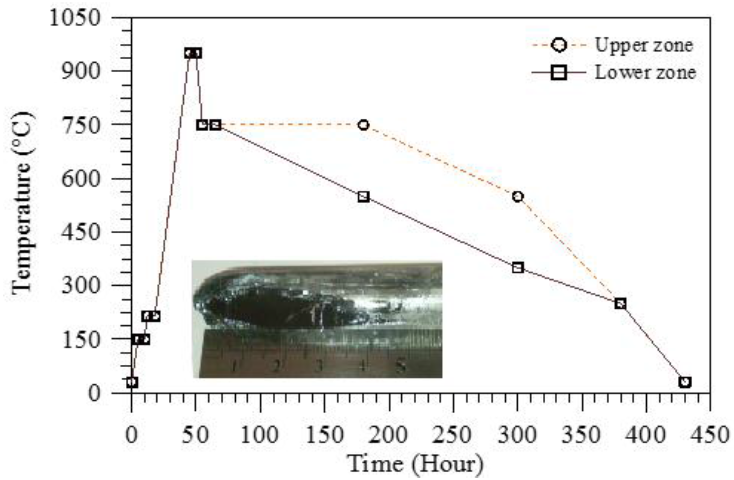
2. Growth
3. Exfoliation
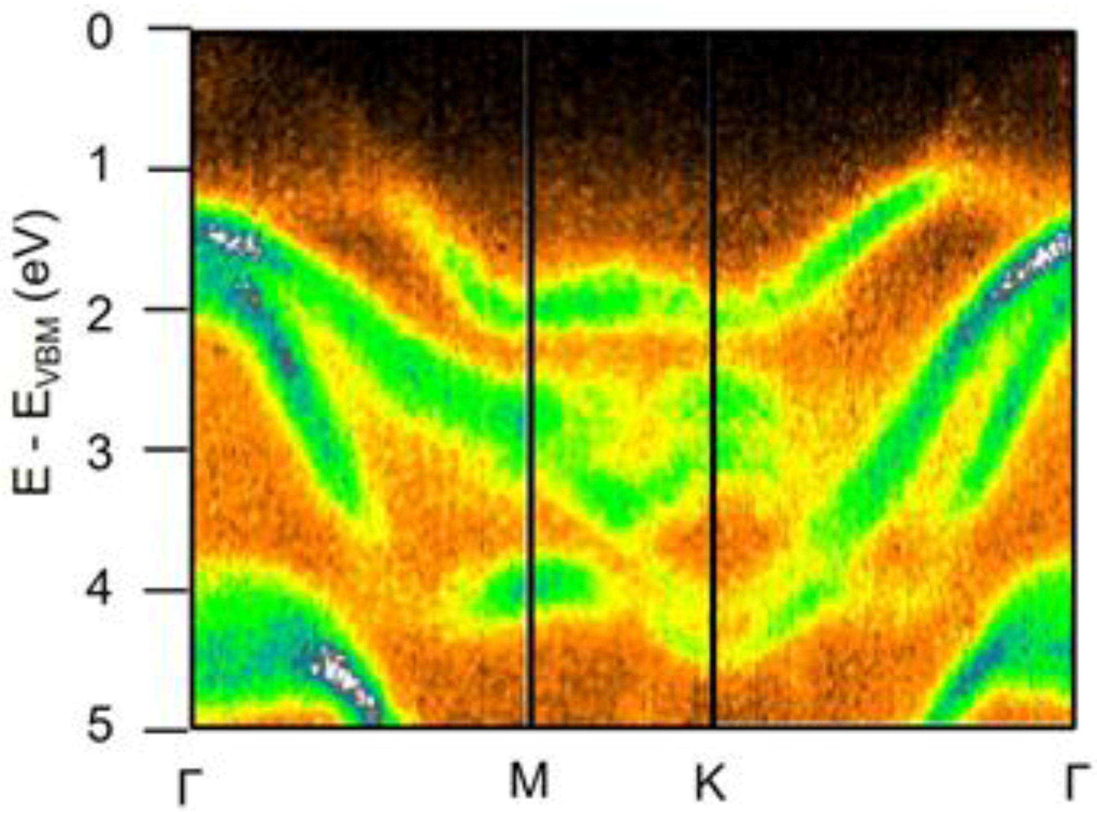
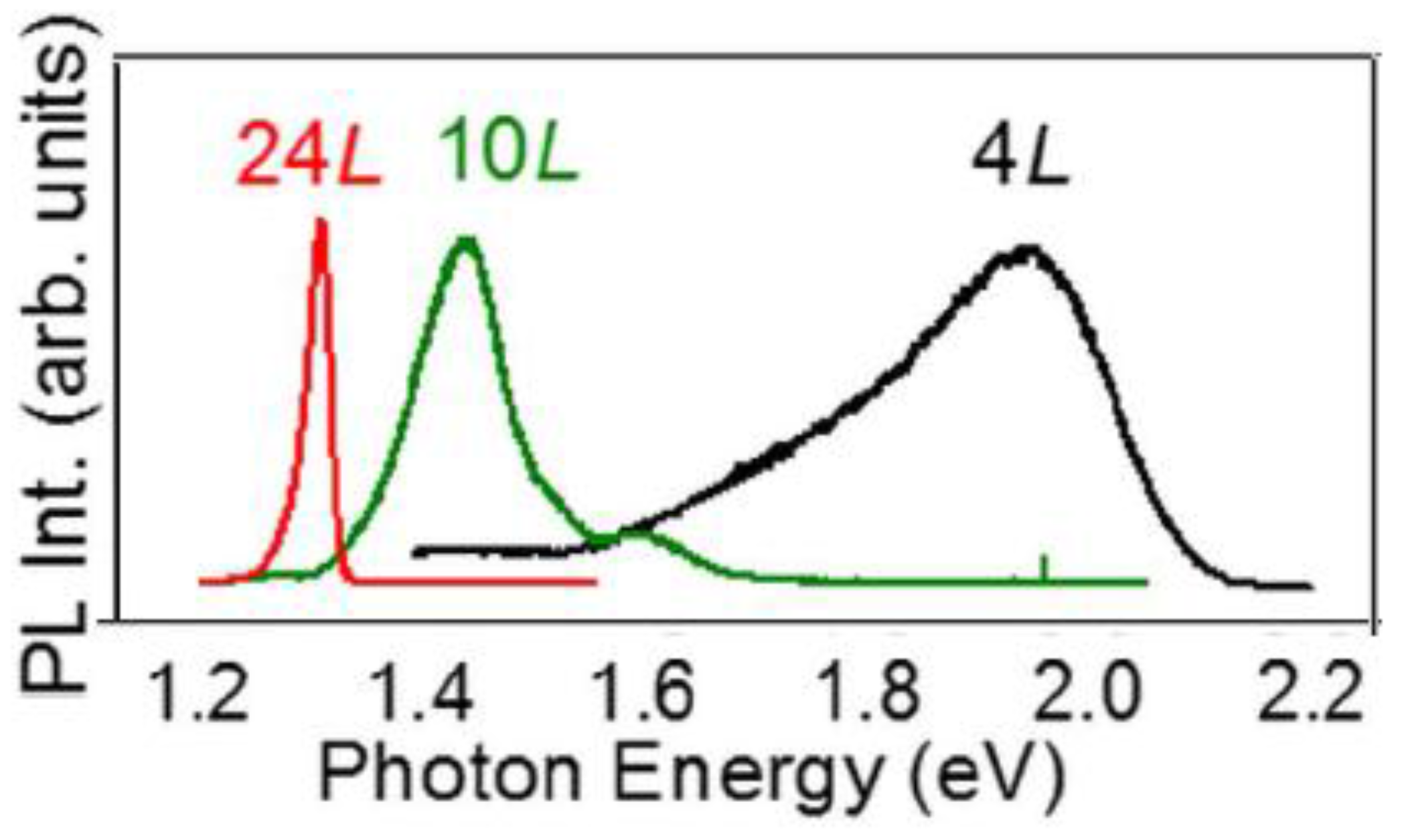
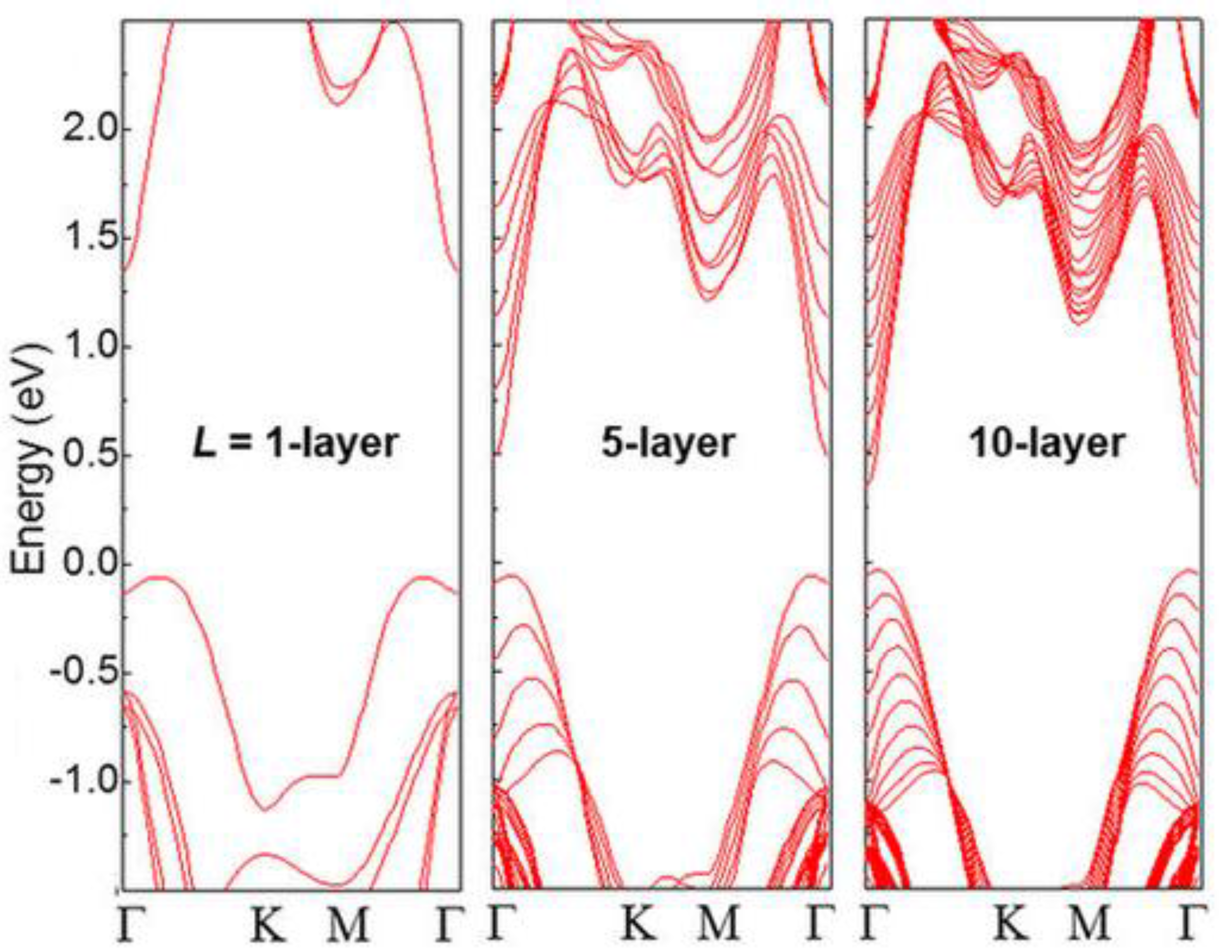
4. Electronic Properties
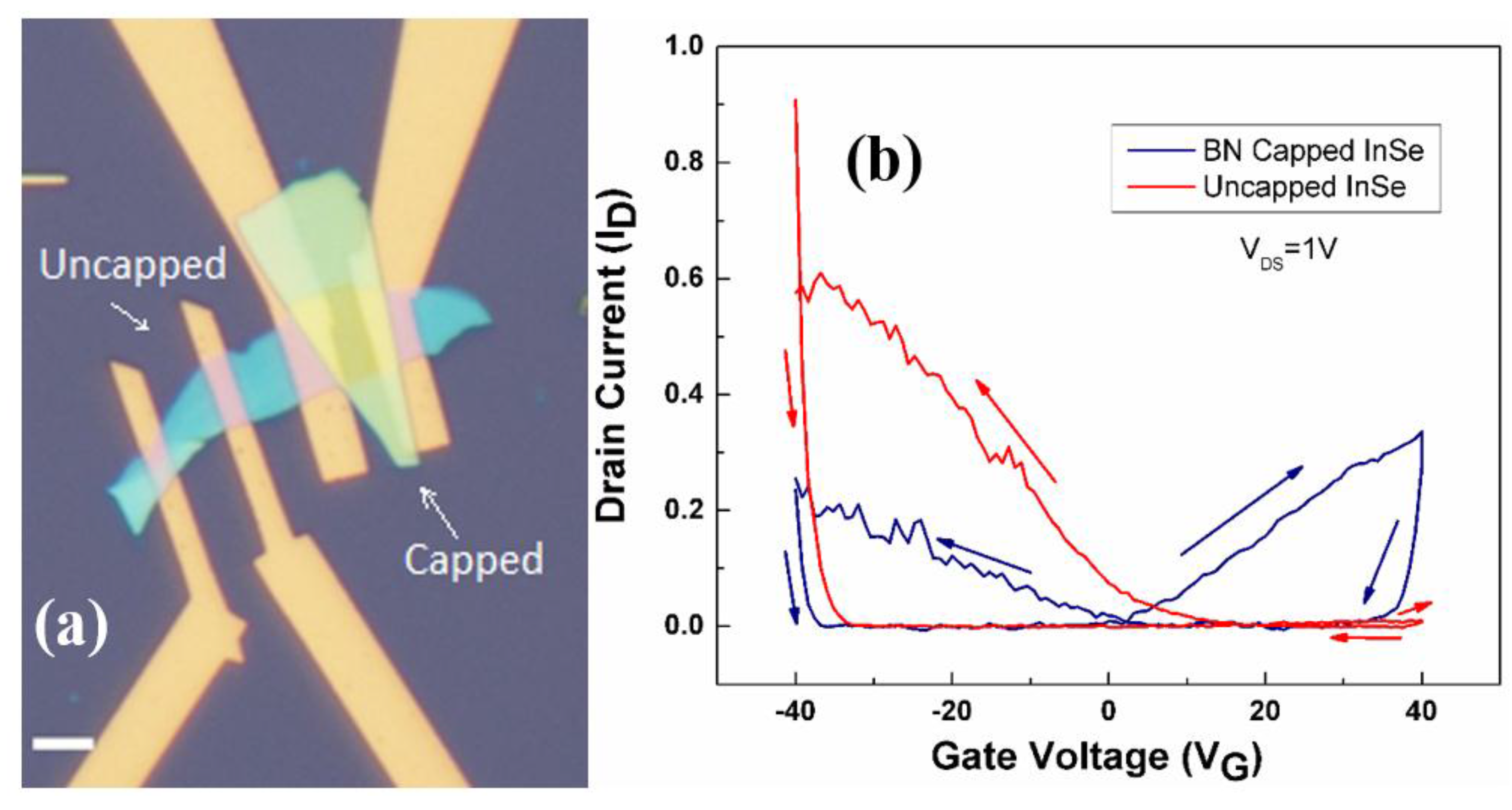
5. Ambient Stability
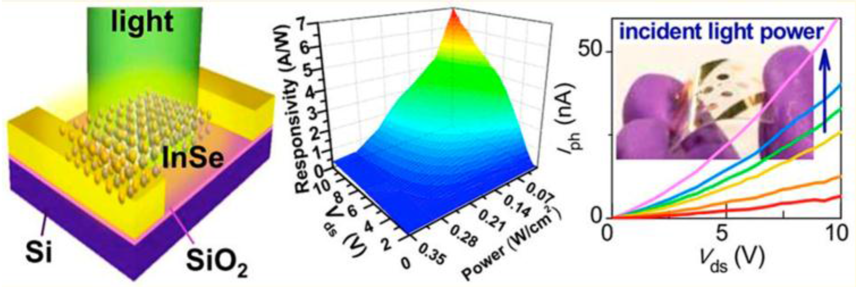
6. Applications
7. Conclusions
Author Contributions
Conflicts of Interest
References
- Buscema, M.; Island, J.O.; Groenendijk, D.J.; Blanter, S.I.; Steele, G.A.; van der Zant, H.S.J.; Castellanos-Gomez, A. Photocurrent generation with two-dimensional van der Waals semiconductors. Chem. Soc. Rev. 2015, 44, 3691–3718. [Google Scholar] [CrossRef] [PubMed]
- Roldán, R.; Castellanos-Gomez, A.; Cappelluti, E.; Guinea, F. Strain engineering in semiconducting two-dimensional crystals. J. Phys. Condens. Matter 2015, 27. [Google Scholar] [CrossRef] [PubMed]
- Scholz, A.; Stauber, T.; Schliemann, J. Plasmons and screening in a monolayer of MoS2. Phys. Rev. B 2013, 88. [Google Scholar] [CrossRef]
- Stauber, T.; Gómez-Santos, G. Plasmons in layered structures including graphene. New J. Phys. 2012, 14. [Google Scholar] [CrossRef]
- Lee, T.H.; Kim, S.Y.; Jang, H.W. Black phosphorus: Critical review and potential for water splitting photocatalyst. Nanomaterials 2016, 6, 194. [Google Scholar] [CrossRef] [PubMed]
- Fiori, G.; Bonaccorso, F.; Iannaccone, G.; Palacios, T.; Neumaier, D.; Seabaugh, A.; Banerjee, S.K.; Colombo, L. Electronics based on two-dimensional materials. Nat. Nanotechnol. 2014, 9, 768–779. [Google Scholar] [CrossRef] [PubMed]
- Koppens, F.H.L.; Mueller, T.; Avouris, P.; Ferrari, A.C.; Vitiello, M.S.; Polini, M. Photodetectors based on graphene, other two-dimensional materials and hybrid systems. Nat. Nanotechnol. 2014, 9, 780–793. [Google Scholar] [CrossRef] [PubMed]
- Lee, J.Y.; Shin, J.H.; Lee, G.H.; Lee, C.H. Two-dimensional semiconductor optoelectronics based on van der Waals heterostructures. Nanomaterials 2016, 6, 193. [Google Scholar] [CrossRef] [PubMed]
- Yang, H.; Qin, S.; Zheng, X.; Wang, G.; Tan, Y.; Peng, G.; Zhang, X. An Al2O3 Gating Substrate for the Greater Performance of Field Effect Transistors Based on Two-Dimensional Materials. Nanomaterials 2017, 7, 286. [Google Scholar] [CrossRef] [PubMed]
- Miro, P.; Audiffred, M.; Heine, T. An atlas of two-dimensional materials. Chem. Soc. Rev. 2014, 43, 6537–6554. [Google Scholar] [CrossRef] [PubMed]
- Bhimanapati, G.R.; Lin, Z.; Meunier, V.; Jung, Y.; Cha, J.; Das, S.; Xiao, D.; Son, Y.; Strano, M.S.; Cooper, V.R.; et al. Recent Advances in Two-Dimensional Materials beyond Graphene. ACS Nano 2015, 9, 11509–11539. [Google Scholar] [CrossRef] [PubMed]
- Akinwande, D.; Petrone, N.; Hone, J. Two-dimensional flexible nanoelectronics. Nat. Commun. 2014, 5. [Google Scholar] [CrossRef] [PubMed]
- Zhu, W.; Yogeesh, M.N.; Yang, S.; Aldave, S.H.; Kim, J.-S.; Sonde, S.; Tao, L.; Lu, N.; Akinwande, D. Flexible Black Phosphorus Ambipolar Transistors, Circuits and AM Demodulator. Nano Lett. 2015, 15, 1883–1890. [Google Scholar] [CrossRef] [PubMed]
- Novoselov, K. Graphene: Mind the gap. Nat. Mater. 2007, 6, 720–721. [Google Scholar] [CrossRef] [PubMed]
- Giubileo, F.; Di Bartolomeo, A.; Martucciello, N.; Romeo, F.; Iemmo, L.; Romano, P.; Passacantando, M. Contact resistance and channel conductance of graphene field-effect transistors under low-energy electron irradiation. Nanomaterials 2016, 6, 206. [Google Scholar] [CrossRef] [PubMed]
- Luongo, G.; Giubileo, F.; Genovese, L.; Iemmo, L.; Martucciello, N.; Di Bartolomeo, A. I-V and C-V Characterization of a High-Responsivity Graphene/Silicon Photodiode with Embedded MOS Capacitor. Nanomaterials 2017, 7, 158. [Google Scholar] [CrossRef] [PubMed]
- Jin, K.; Zhou, X.; Liu, Z. Graphene/sulfur/carbon nanocomposite for high performance lithium-sulfur batteries. Nanomaterials 2015, 5, 1481–1492. [Google Scholar] [CrossRef] [PubMed]
- Wang, X.; Huang, L.; Peng, Y.; Huo, N.; Wu, K.; Xia, C.; Wei, Z.; Tongay, S.; Li, J. Enhanced rectification, transport property and photocurrent generation of multilayer ReSe2/MoS2 p–n heterojunctions. Nano Res. 2015, 9, 507–516. [Google Scholar] [CrossRef]
- Bandurin, D.A.; Tyurnina, A.V.; Yu, G.L.; Mishchenko, A.; Zolyomi, V.; Morozov, S.V.; Kumar, R.K.; Gorbachev, R.V.; Kudrynskyi, Z.R.; Pezzini, S.; et al. High electron mobility, quantum Hall effect and anomalous optical response in atomically thin InSe. Nat. Nanotechnol. 2017, 12, 223–227. [Google Scholar] [CrossRef] [PubMed]
- Politano, A.; Chiarello, G.; Samnakay, R.; Liu, G.; Gurbulak, B.; Duman, S.; Balandin, A.A.; Boukhvalov, D.W. The influence of chemical reactivity of surface defects on ambient-stable InSe-based nanodevices. Nanoscale 2016, 8, 8474–8479. [Google Scholar] [CrossRef] [PubMed]
- Mosca, D.H.; Mattoso, N.; Lepienski, C.M.; Veiga, W.; Mazzaro, I.; Etgens, V.H.; Eddrief, M. Mechanical properties of layered InSe and GaSe single crystals. J. Appl. Phys. 2002, 91, 140–144. [Google Scholar] [CrossRef]
- Ho, C.-H.; Chu, Y.-J. Bending Photoluminescence and Surface Photovoltaic Effect on Multilayer InSe 2D Microplate Crystals. Adv. Opt. Mater. 2015, 3, 1750–1758. [Google Scholar] [CrossRef]
- Tamalampudi, S.R.; Lu, Y.Y.; Kumar, R.; Sankar, R.; Liao, C.D.; Moorthy, K.; Cheng, C.H.; Chou, F.C.; Chen, Y.T. High performance and bendable few-layered InSe photodetectors with broad spectral response. Nano Lett. 2014, 14, 2800–2806. [Google Scholar] [CrossRef] [PubMed]
- Ho, P.-H.; Chang, Y.-R.; Chu, Y.-C.; Li, M.-K.; Tsai, C.-A.; Wang, W.-H.; Ho, C.-H.; Chen, C.-W.; Chiu, P.-W. High-Mobility InSe Transistors: The Role of Surface Oxides. ACS Nano 2017, 11, 7362–7370. [Google Scholar] [CrossRef] [PubMed]
- Mudd, G.W.; Svatek, S.A.; Hague, L.; Makarovsky, O.; Kudrynskyi, Z.R.; Mellor, C.J.; Beton, P.H.; Eaves, L.; Novoselov, K.S.; Kovalyuk, Z.D.; et al. High Broad-Band Photoresponsivity of Mechanically Formed InSe–Graphene van der Waals Heterostructures. Adv. Mater. 2015, 27, 3760–3766. [Google Scholar] [CrossRef] [PubMed]
- Mudd, G.W.; Svatek, S.A.; Ren, T.; Patanè, A.; Makarovsky, O.; Eaves, L.; Beton, P.H.; Kovalyuk, Z.D.; Lashkarev, G.V.; Kudrynskyi, Z.R.; et al. Tuning the bandgap of exfoliated InSe nanosheets by quantum confinement. Adv. Mater. 2013, 25, 5714–5718. [Google Scholar] [CrossRef] [PubMed]
- Lin, Z.; Karthik, P.S.; Hada, M.; Nishikawa, T.; Hayashi, Y. Simple technique of exfoliation and dispersion of multilayer graphene from natural graphite by ozone-assisted sonication. Nanomaterials 2017, 7, 125. [Google Scholar] [CrossRef] [PubMed]
- Sánchez-Royo, J.F.; Muñoz-Matutano, G.; Brotons-Gisbert, M.; Martínez-Pastor, J.P.; Segura, A.; Cantarero, A.; Mata, R.; Canet-Ferrer, J.; Tobias, G.; Canadell, E.; et al. Electronic structure, optical properties, and lattice dynamics in atomically thin indium selenide flakes. Nano Res. 2014, 7, 1556–1568. [Google Scholar] [CrossRef]
- Ho, C.-H. Thickness-dependent carrier transport and optically enhanced transconductance gain in III–VI multilayer InSe. 2D Mater. 2016, 3. [Google Scholar] [CrossRef]
- Sucharitakul, S.; Goble, N.J.; Kumar, U.R.; Sankar, R.; Bogorad, Z.A.; Chou, F.-C.; Chen, Y.-T.; Gao, X.P.A. Intrinsic Electron Mobility Exceeding 103 cm2/(V·s) in Multilayer InSe FETs. Nano Lett. 2015, 15, 3815–3819. [Google Scholar] [CrossRef] [PubMed]
- Lei, S.; Wen, F.; Ge, L.; Najmaei, S.; George, A.; Gong, Y.; Gao, W.; Jin, Z.; Li, B.; Lou, J.; et al. An Atomically Layered InSe Avalanche Photodetector. Nano Lett. 2015, 15, 3048–3055. [Google Scholar] [CrossRef] [PubMed]
- Chen, Z.; Biscaras, J.; Shukla, A. A high performance graphene/few-layer InSe photo-detector. Nanoscale 2015, 7, 5981–5986. [Google Scholar] [CrossRef] [PubMed]
- Ma, Y.; Dai, Y.; Yu, L.; Niu, C.; Huang, B. Engineering a topological phase transition in β-InSe via strain. New J. Phys. 2013, 15. [Google Scholar] [CrossRef]
- Yüksek, M.; Yaglioglu, H.G.; Elmali, A.; Aydin, E.M.; Kürüm, U.; Ateş, A. Nonlinear and saturable absorption characteristics of Ho doped InSe crystals. Opt. Commun. 2014, 310, 100–103. [Google Scholar] [CrossRef]
- Han, G.; Chen, Z.-G.; Drennan, J.; Zou, J. Indium Selenides: Structural Characteristics, Synthesis and Their Thermoelectric Performances. Small 2014, 10, 2747–2765. [Google Scholar] [CrossRef] [PubMed]
- Lei, S.; Ge, L.; Najmaei, S.; George, A.; Kappera, R.; Lou, J.; Chhowalla, M.; Yamaguchi, H.; Gupta, G.; Vajtai, R.; et al. Evolution of the Electronic Band Structure and Efficient Photo-Detection in Atomic Layers of InSe. ACS Nano 2014, 8, 1263–1272. [Google Scholar] [CrossRef] [PubMed]
- Gürbulak, B.; Şata, M.; Dogan, S.; Duman, S.; Ashkhasi, A.; Keskenler, E.F. Structural characterizations and optical properties of InSe and InSe: Ag semiconductors grown by Bridgman/Stockbarger technique. Physica E 2014, 64, 106–111. [Google Scholar] [CrossRef]
- Mudd, G.W.; Patanè, A.; Kudrynskyi, Z.R.; Fay, M.W.; Makarovsky, O.; Eaves, L.; Kovalyuk, Z.D.; Zólyomi, V.; Falko, V. Quantum confined acceptors and donors in InSe nanosheets. Appl. Phys. Lett. 2014, 105. [Google Scholar] [CrossRef] [Green Version]
- Zhirko, Y.; Trachevsky, V.; Kovalyuk, Z. On the Possibility of Layered Crystals Application for Solid State Hydrogen Storages—InSe and GaSe Crystals. In Hydrogen Storage; InTech: Rijeka, Croatia, 2012. [Google Scholar]
- Julien, C.M.; Balkanski, M. Lithium reactivity with III–VI layered compounds. Mater. Sci. Eng. B 2003, 100, 263–270. [Google Scholar] [CrossRef]
- Viti, L.; Hu, J.; Coquillat, D.; Knap, W.; Tredicucci, A.; Politano, A.; Vitiello, M.S. Black Phosphorus Terahertz Photodetectors. Adv. Mater. 2015, 27, 5567–5572. [Google Scholar] [CrossRef] [PubMed]
- El-Sayed, S. Optical investigations of the indium selenide glasses. Vacuum 2003, 72, 169–175. [Google Scholar] [CrossRef]
- Emery, J.Y.; Brahim-Ostmane, L.; Hirlimann, C.; Chevy, A. Reflection high-energy electron diffraction studies of InSe and GaSe layered compounds grown by molecular beam epitaxy. J. Appl. Phys. 1992, 71, 3256–3259. [Google Scholar] [CrossRef]
- Lauth, J.; Kulkarni, A.; Spoor, F.C.M.; Renaud, N.; Grozema, F.C.; Houtepen, A.J.; Schins, J.M.; Kinge, S.; Siebbeles, L.D.A. Photogeneration and Mobility of Charge Carriers in Atomically Thin Colloidal InSe Nanosheets Probed by Ultrafast Terahertz Spectroscopy. J. Phys. Chem. Lett. 2016, 7, 4191–4196. [Google Scholar] [CrossRef] [PubMed]
- Lauth, J.; Gorris, F.E.S.; Samadi Khoshkhoo, M.; Chassé, T.; Friedrich, W.; Lebedeva, V.; Meyer, A.; Klinke, C.; Kornowski, A.; Scheele, M.; et al. Solution-Processed Two-Dimensional Ultrathin InSe Nanosheets. Chem. Mater. 2016, 28, 1728–1736. [Google Scholar] [CrossRef]
- Julien, C.; Samaras, I.; Tsakiri, M.; Dzwonkowski, P.; Balkanski, M. Lithium insertion in InSe films and applications in microbatteries. Mater. Sci. Eng. B 1989, 3, 25–29. [Google Scholar] [CrossRef]
- Park, J.-H.; Afzaal, M.; Helliwell, M.; Malik, M.A.; O’Brien, P.; Raftery, J. Chemical vapor deposition of indium selenide and gallium selenide thin films from mixed alkyl/dialkylselenophosphorylamides. Chem. Mater. 2003, 15, 4205–4210. [Google Scholar] [CrossRef]
- Lang, O.; Klein, A.; Schlaf, R.; Löher, T.; Pettenkofer, C.; Jaegermann, W.; Chevy, A. InSeGaSe heterointerfaces prepared by Van der Waals epitaxy. J. Cryst. Growth 1995, 146, 439–443. [Google Scholar] [CrossRef]
- Shigetomi, S.; Ikari, T. Crystalline InSe films prepared by RF-sputtering technique. Jpn. J. Appl. Phys. 1991, 30, L2127. [Google Scholar] [CrossRef]
- Chevy, A.; Gouskov, A.; Besson, J. Growth of crystalline slabs of layered InSe by the Czochralski method. J. Cryst. Growth 1978, 43, 756–759. [Google Scholar] [CrossRef]
- De Blasi, C.; Micocci, G.; Mongelli, S.; Tepore, A. Large InSe single crystals grown from stoichiometric and non-stoichiometric melts. J. Cryst. Growth 1982, 57, 482–486. [Google Scholar] [CrossRef]
- Chevy, A. Improvement of growth parameters for Bridgman-grown InSe crystals. J. Cryst. Growth 1984, 67, 119–124. [Google Scholar] [CrossRef]
- Hoshino, H.; Schmutzler, R.W.; Hensel, F. The High Temperature Vapour Pressure Curve and the Critical Point of Liquid Selenium. Ber. Bunsenges. Phys. Chem. 1976, 80, 27–31. [Google Scholar] [CrossRef]
- Shigetomi, S.; Ikari, T. Electrical and optical properties of n- and p-InSe doped with Sn and As. J. Appl. Phys. 2003, 93, 2301–2303. [Google Scholar] [CrossRef]
- Duman, S.; Elkoca, Z.; Gurbulak, B.; Bahtiyari Tekle, T.; Dogan, S. Metal/p-InSe:Mn Schottky barrier diodes. J. Optoelectron. Adv. Mater. 2012, 14, 693–698. [Google Scholar]
- Duman, S.; Gürbulak, B.; Doǧan, S.; Türüt, A. Electrical characteristics and inhomogeneous barrier analysis of Au–Be/p-InSe:Cd Schottky barrier diodes. Microelectron. Eng. 2009, 86, 106–110. [Google Scholar] [CrossRef]
- Duman, S.; Gurbulak, B.; Turut, A. Temperature-dependent optical absorption measurements and Schottky contact behavior in layered semiconductor n-type InSe(:Sn). Appl. Surf. Sci. 2007, 253, 3899–3905. [Google Scholar] [CrossRef]
- Gürbulak, B.; Kundakçi, M.; Ateş, A.; Yildirim, M. Electric field influence on exciton absorption of Er doped and undoped InSe single crystals. Phys. Scr. 2007, 75, 424–430. [Google Scholar] [CrossRef]
- Gürbulak, B. Urbach tail and optical investigations of Gd doped and undoped InSe single crystals. Phys. Scr. 2004, 70, 197–201. [Google Scholar] [CrossRef]
- Ateş, A.; Yildirim, M.; Gürbulak, B. Investigation of the electrical properties of Ho-doped InSe single crystal. Physica E 2004, 21, 85–90. [Google Scholar] [CrossRef]
- Shigetomi, S.; Ikari, T. Impurity levels in layered semiconductor n-InSe doped with Ge. Phys. Status Solidi B 2003, 236, 135–142. [Google Scholar] [CrossRef]
- Shigetomi, S.; Ikari, T. Optical and Electrical Characteristics of Layered Semiconductor p-InSe Doped with Sb. Jpn. J. Appl. Phys. Part 1 2003, 42, 6951–6954. [Google Scholar] [CrossRef]
- Shigetomi, S.; Ikari, T. Optical and electrical properties of layer semiconductor n-InSe doped with Sn. Jpn. J. Appl. Phys. Part 1 2002, 41, 5565–5566. [Google Scholar] [CrossRef]
- Shigetomi, S.; Ikari, T. Annealing behavior of layer semiconductor p-InSe doped with Hg. Jpn. J. Appl. Phys. Part 1 2000, 39, 1184–1185. [Google Scholar] [CrossRef]
- Gürbulak, B.; Yildirim, M.; Ateç, A.; Doǧan, S.; Yoǧurtçu, Y.K. Growth and Temperature Dependence of Optical Properties of Er Doped and Undoped n-Type InSe. Jpn. J. Appl. Phys. Part 1 1999, 38, 5133–5136. [Google Scholar] [CrossRef]
- Gürbulak, B. Growth and optical properties of Dy doped and undoped n-type InSe single crystal. Solid State Commun. 1999, 109, 665–669. [Google Scholar] [CrossRef]
- Shigetomi, S.; Ikari, T.; Nakashima, H. Impurity levels in p-type layered semiconductor InSe doped with Hg. Phys. Status Solidi B 1998, 209, 93–99. [Google Scholar] [CrossRef]
- Politano, A.; Campi, D.; Cattelan, M.; Ben Amara, I.; Jaziri, S.; Mazzotti, A.; Barinov, A.; Gürbulak, B.; Duman, S.; Agnoli, S.; et al. Indium selenide: An insight on electronic band structure and surface excitations. Sci. Rep. 2017, 7. [Google Scholar] [CrossRef] [PubMed]
- Mudd, G.W.; Molas, M.R.; Chen, X.; Zólyomi, V.; Nogajewski, K.; Kudrynskyi, Z.R.; Kovalyuk, Z.D.; Yusa, G.; Makarovsky, O.; Eaves, L.; et al. The direct-to-indirect band gap crossover in two-dimensional van der Waals Indium Selenide crystals. Sci. Rep. 2016, 6. [Google Scholar] [CrossRef] [PubMed]
- Kong, D.; Cha, J.J.; Lai, K.; Peng, H.; Analytis, J.G.; Meister, S.; Chen, Y.; Zhang, H.J.; Fisher, I.R.; Shen, Z.X.; Cui, Y. Rapid surface oxidation as a source of surface degradation factor for Bi2Se3. ACS Nano 2011, 5, 4698–4703. [Google Scholar] [CrossRef] [PubMed]
- Island, J.O.; Steele, G.A.; van der Zant, H.S.J.; Castellanos-Gomez, A. Environmental instability of few-layer black phosphorus. 2D Mater. 2015, 2. [Google Scholar] [CrossRef]
- Politano, A.; Chiarello, G. Enhancement of hydrolysis in alkali ultrathin layers on metal substrates in the presence of electron confinement. Chem. Phys. Lett. 2010, 494, 84–87. [Google Scholar] [CrossRef]
- Henderson, M.A. The interaction of water with solid surfaces: Fundamental aspects revisited. Surf. Sci. Rep. 2002, 46, 1–308. [Google Scholar] [CrossRef]
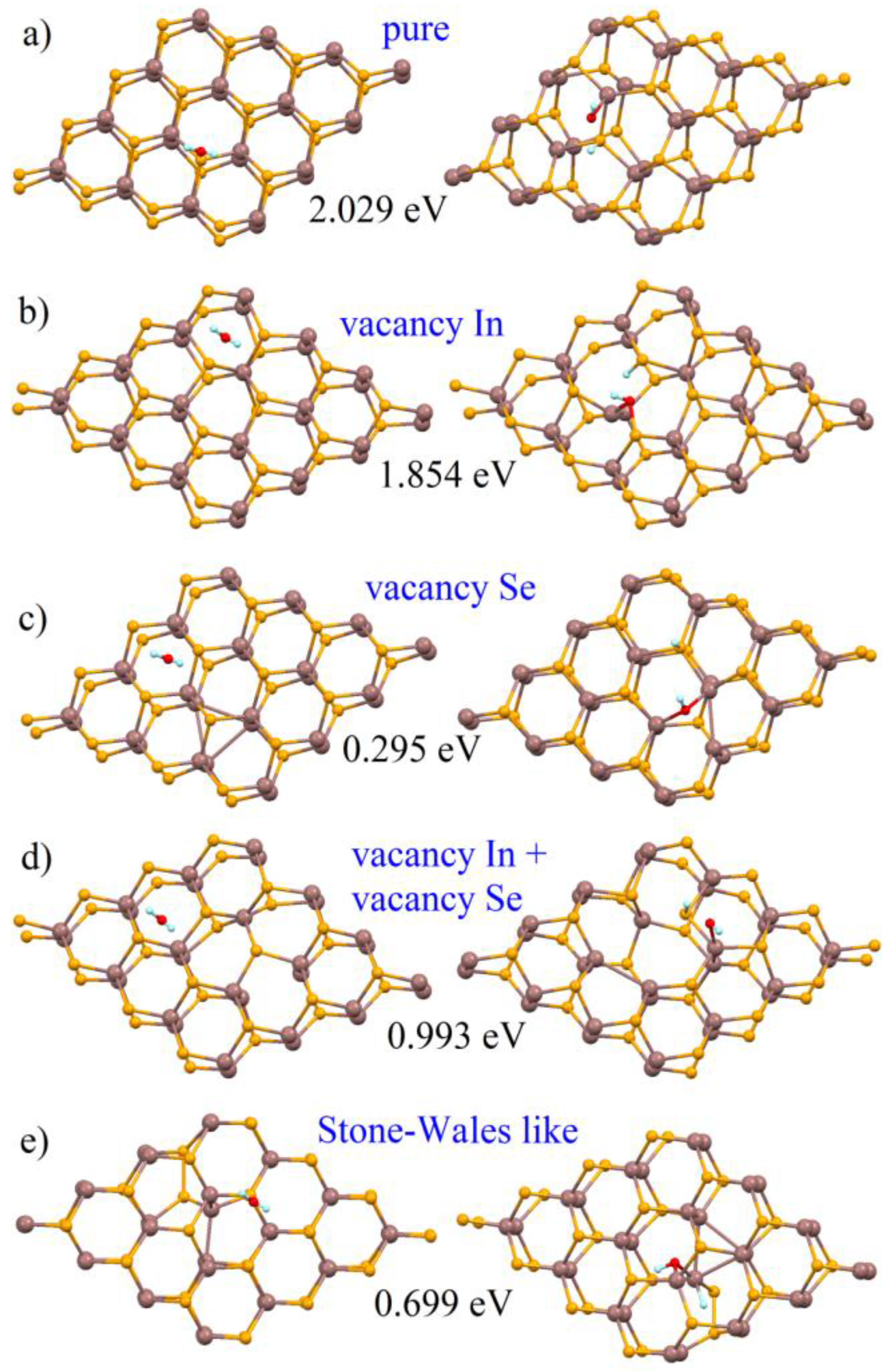
- Shi, L.; Zhou, Q.; Zhao, Y.; Ouyang, Y.; Ling, C.; Li, Q.; Wang, J. Oxidation mechanism and protection strategy of ultrathin Indium Selenide: Insight from Theory. J. Phys. Chem. Lett. 2017, 8, 4368–4373. [Google Scholar] [CrossRef] [PubMed]
- Xiao, K.; Carvalho, A.; Neto, A.C. Defects and oxidation resilience in InSe. Phys. Rev. B 2017, 96. [Google Scholar] [CrossRef]
- Cai, Y.; Zhang, G.; Zhang, Y.-W. Charge Transfer and Functionalization of Monolayer InSe by Physisorption of Small Molecules for Gas Sensing. J. Phys. Chem. C 2017, 121, 10182–10193. [Google Scholar] [CrossRef]
- Ma, D.; Ju, W.; Tang, Y.; Chen, Y. First-principles study of the small molecule adsorption on the InSe monolayer. Appl. Surf. Sci. 2017, 426, 244–252. [Google Scholar] [CrossRef]
- Peng, Q.; Xiong, R.; Sa, B.; Zhou, J.; Wen, C.; Wu, B.; Anpo, M.; Sun, Z. Computational mining of photocatalysts for water splitting hydrogen production: Two-Dimensional InSe-family monolayers. Catal. Sci. Technol. 2017, 7, 2744–2752. [Google Scholar] [CrossRef]
- Guo, Y.; Zhou, S.; Bai, Y.; Zhao, J. Enhanced piezoelectric effect in Janus group-III chalcogenide monolayers. Appl. Phys. Lett. 2017, 110, 163102. [Google Scholar] [CrossRef]
- Jin, H.; Li, J.; Dai, Y.; Wei, Y. Engineering the electronic and optoelectronic properties of InX (X = S, Se, Te) monolayers via strain. Phys. Chem. Chem. Phys. 2017, 19, 4855–4860. [Google Scholar] [CrossRef] [PubMed]
- Quan, L.; Song, Y.; Lin, Y.; Zhang, G.; Dai, Y.; Wu, Y.; Jin, K.; Ding, H.; Pan, N.; Luo, Y. The Raman enhancement effect on a thin GaSe flake and its thickness dependence. J. Mater. Chem. C 2015, 3, 11129–11134. [Google Scholar] [CrossRef]
- Boukhvalov, D.W.; Katsnelson, M.I. Chemical Functionalization of Graphene with Defects. Nano Lett. 2008, 8, 4373–4379. [Google Scholar] [CrossRef] [PubMed]
- Boukhvalov, D.W.; Dreyer, D.R.; Bielawski, C.W.; Son, Y.-W. A Computational Investigation of the Catalytic Properties of Graphene Oxide: Exploring Mechanisms by using DFT Methods. ChemCatChem 2012, 4, 1844–1849. [Google Scholar] [CrossRef]
- Gordillo, G.; Calderón, C. CIS thin film solar cells with evaporated InSe buffer layers. Sol. Energy Mater. Sol. Cells 2003, 77, 163–173. [Google Scholar] [CrossRef]
- Segura, A.; Chevy, A.; Guesdon, J.P.; Besson, J.M. Photovoltaic efficiency of InSe solar cells. Sol. Energy Mater. 1979, 2, 159–165. [Google Scholar] [CrossRef]
- Damodara Das, V.; Sathyanarayanan, J.; Damodare, L. Effect of annealing and surface treatment on the efficiency of photoelectrochemical (PEC) solar cells with vacuum-deposited n-InSe thin film electrode. Surf. Coat. Technol. 1997, 94–95, 669–671. [Google Scholar]
- Kovalyuk, Z.; Katerynchuk, V.; Savchuk, A.; Sydor, O. Intrinsic conductive oxide–p-InSe solar cells. Mater. Sci. Eng. B 2004, 109, 252–255. [Google Scholar] [CrossRef]
- Darwish, A.; Hanafy, T.; Attia, A.; Habashy, D.; El-Bakry, M.; El-Nahass, M. Optoelectronic performance and artificial neural networks (ANNs) modeling of n-InSe/p-Si solar cell. Superlattices Microstruct. 2015, 83, 299–309. [Google Scholar] [CrossRef]
- Mandal, K.C.; Das, S. Fabrication and characterization of improved p-GaTe/n-InSe heterojunction solar cells. In Proceedings of the 2012 38th IEEE Photovoltaic Specialists Conference (PVSC), Austin, TX, USA, 3–8 June 2012; pp. 000177–000180. [Google Scholar]
- Mönch, W. Interface States. In Semiconductor Surfaces and Interfaces; Springer: Berlin, Germany, 2013; Volume 26, pp. 81–103. [Google Scholar]
- Ando, K.; Katsui, A. Optical properties and photovoltaic device applications of InSe films. Thin Solid Films 1981, 76, 141–148. [Google Scholar] [CrossRef]
- Balakrishnan, N.; Kudrynskyi, Z.R.; Fay, M.W.; Mudd, G.W.; Svatek, S.A.; Makarovsky, O.; Kovalyuk, Z.D.; Eaves, L.; Beton, P.H.; Patanè, A. Room Temperature Electroluminescence from Mechanically Formed van der Waals III-VI Homojunctions and Heterojunctions. Adv. Opt. Mater. 2014, 2, 1064–1069. [Google Scholar] [CrossRef]
- Chen, X.B.; Kelley, D.F. Photophysics of GaSe/InSe nanoparticle heterojunctions. J. Phys. Chem. B 2006, 110, 25259–25265. [Google Scholar] [CrossRef] [PubMed]
- Brotons-Gisbert, M.; Andres-Penares, D.; Suh, J.; Hidalgo, F.; Abargues, R.; Rodríguez-Cantó, P.J.; Segura, A.; Cros, A.; Tobias, G.; Canadell, E. Nanotexturing to enhance photoluminescent response of atomically thin indium selenide with highly tunable band gap. Nano Lett. 2016, 16, 3221–3229. [Google Scholar] [CrossRef] [PubMed]


| Species/Adsorption Site | Hole (eV) | Top (eV) |
|---|---|---|
| H2O | −0.139 | 0.69 |
| CO | 0.014 | 2.75 |
| CO2 | 0.244 | 2.05 |
| N2 | 0.097 | 1.15 |
| O2 | 0.705 | 3.67 |
© 2017 by the authors. Licensee MDPI, Basel, Switzerland. This article is an open access article distributed under the terms and conditions of the Creative Commons Attribution (CC BY) license (http://creativecommons.org/licenses/by/4.0/).
Share and Cite
Boukhvalov, D.W.; Gürbulak, B.; Duman, S.; Wang, L.; Politano, A.; Caputi, L.S.; Chiarello, G.; Cupolillo, A. The Advent of Indium Selenide: Synthesis, Electronic Properties, Ambient Stability and Applications. Nanomaterials 2017, 7, 372. https://doi.org/10.3390/nano7110372
Boukhvalov DW, Gürbulak B, Duman S, Wang L, Politano A, Caputi LS, Chiarello G, Cupolillo A. The Advent of Indium Selenide: Synthesis, Electronic Properties, Ambient Stability and Applications. Nanomaterials. 2017; 7(11):372. https://doi.org/10.3390/nano7110372
Chicago/Turabian StyleBoukhvalov, Danil W., Bekir Gürbulak, Songül Duman, Lin Wang, Antonio Politano, Lorenzo S. Caputi, Gennaro Chiarello, and Anna Cupolillo. 2017. "The Advent of Indium Selenide: Synthesis, Electronic Properties, Ambient Stability and Applications" Nanomaterials 7, no. 11: 372. https://doi.org/10.3390/nano7110372
APA StyleBoukhvalov, D. W., Gürbulak, B., Duman, S., Wang, L., Politano, A., Caputi, L. S., Chiarello, G., & Cupolillo, A. (2017). The Advent of Indium Selenide: Synthesis, Electronic Properties, Ambient Stability and Applications. Nanomaterials, 7(11), 372. https://doi.org/10.3390/nano7110372